
Abstract
The upcoming beyond-5G and 6G ultra-high speed transmission networks have urged photonic transceivers to allow for higher bandwidth performance. In this work, an evanescent coupled high speed waveguide photodetector (PD) is fabricated and analyzed. Adopting a modified uni-traveling carrier structure, the PD exhibits a bandwidth of 100 GHz and a low dark current of 3 nA at −1.5 V. Numerical simulations show that the measured responsivity of 0.25 A W−1 is worsened by the inaccurate cleaving length of the coupling waveguide, and could potentially reach 0.688 A W−1 with anti-reflection film at the facet. The bandwidth is bound by high resistance and capacitance giving a transit-time limit as high as 310 GHz.
Export citation and abstract BibTeX RIS

Content from this work may be used under the terms of the Creative Commons Attribution 4.0 license. Any further distribution of this work must maintain attribution to the author(s) and the title of the work, journal citation and DOI.
Extensive deployment of high-capacity 5G networks and the unrelenting growth in network traffic has urged the optical communication industry to upgrade photonic module performance unceasingly. Current 40/100/400 Gbd module plans have explored high-order modulation formats and coherent technologies to meet the massive throughput need in data-centers, interconnect, access and metro networks. 1,2) Thanks to the efficient methods such as time/wavelength division multiplexing, optical modules with a moderate speed of 10/25/40 Gbd could be arrayed and stacked to expand aggregate capacity. 3–5) For the next generation of 800 Gbd or more optical modules, however, higher baud-rate over 100 Gbd per lane seems necessary for photonic chips and components on the grounds that present digital signal proccessing (DSP) units have already confronted huge pressures regarding cost and power consumption restrictions. 6–10) Particularly in a typical QPSK receiver, the photodetector (PD) bandwidth has reached 65 GHz to cope with 100 Gbd per lane demand. 11) Higher symbol rates towards 200 Gbd or more are under test by the industry. 12,13)
Uni-traveling carrier (UTC) photodetectors have been promoted for potential ultra-high bandwidth applications. 14–16) They utilize the electron overshoot velocity and hole relaxation to reduce the total carrier transit time, meanwhile featuring high response linearity. A drawback of this structure is relatively low responsivity to the conventional P-I-N doping type structure due to the compressed absorption layer, 17,18) and thus the appearance of a modified UTC structure with a cliff layer to balance carrier transit-times and quantum efficiency. 19–21)
In this work, a waveguide PD with a 100 GHz bandwidth is reported. The modified UTC structure is utilized and an edge-coupled evanescent optical plan is also adopted instead of the surface illumination, which not only requires higher fabrication precision for small area structures, but also benefits from a longer absorption length. Optoelectronic simulations, together with experienced formulas, are used to analyse and explain the device performances.
The PD is schematically depicted in Fig. 1(a) with its epitaxial details explained in Table I. A 50 nm absorption layer is lightly N-doped to ensure a partial depletion, and another 110 part is gradually P-doped for electron acceleration. A 20 nm moderate N-doped (1.0 × 1017cm−3) InP is inserted between the InP collector layer and InGaAsP band-gap grading layers to lift up the electric field in the depleted absorber and fasten electron thermal emission into the collector. An evanescent optical coupling is realized from the coupling waveguide to the PD ridge, where the coupling waveguide is comprised of a diluted waveguide of 11 pairs of InGaAsP (Q1.06)/InP layers and a two-layer slab waveguide of 770 nm InGaAsP (Q1.18 + Q1.32). The upper slab waveguide of the higher refractive index facilitates optical power concentration near the roof of the coupling waveguide and thus better evanescent excitation. Meanwhile, the slab waveguide layers are N-doped to act as N-type contact layers of the PD. The Q1.06-InGaAsP layers in the diluted waveguide increase epitaxially from 100 nm to 300 nm, while the InP layers remain at 80 nm, which adds to a total thickness of 3080 nm. Considering a 4.0 μm mode diameter of the tapered fiber output, a wider waveguide of 5.0 μm is proposed for larger coupled input power. The PD ridge is of the same width taking into account a minimized junction area but still has enough length of 10 μm for photo-absorption, since a higher power loss will take place with a narrower PD ridge.

Fig. 1. (a) Schematic of the waveguide PD. (b) Photograph of the fabricated chip.
Download figure:
Standard image High-resolution imageTable I. Epitaxial details of the waveguide PD.
| Composition-Thickness | Doping [cm−3] | Function |
|---|---|---|
| In0.53Ga0.47As-80 nm | P-2.0 × 10¹⁹ | P-contact |
| InGaAsP(Q1.1)-310 nm | P-3.0 × 10¹⁸ | electron barrier |
| InGaAsP-20 nm | P-5.0 × 10¹⁸ | band-gap grading |
| In0.53Ga0.47As-110 nm | P-gradual | p-doped absorber |
| In0.53Ga0.47As-50 nm | N-1.0 × 10¹⁶ | depleted absorber |
| InGaAsP-30 nm | N-1.0 × 10¹⁶ | band-gap grading |
| InP-20 nm | N-1.0 × 10¹⁷ | cliff layer |
| InP-160 nm | N-1.0 × 10¹⁶ | collector |
| InGaAsP(Q1.32)-250 nm | N-5.0 × 10¹⁸ | upper slab waveguide |
| InGaAsP(Q1.18)-520 nm | N-2.0 × 10¹⁸ | down slab waveguide |
| InGaAsP(Q1.06)/InP-3080 nm | U.I.D | diluted waveguide |
| InP-380 μm | S.I. | substrate |
The fabricated chip is photographed in Fig. 1(b). The fabrication process starts with Pt/Ti/Pt/Au P-type contact definition by electronic beam evaporation. The PD ridge is then etched by the induced-coupled plasma (ICP) method. The N-type contact is formed by Ni/Ge/Au sputtering and lift-off, followed by ICP-etching of the coupling waveguide. The coplanar waveguide lines (CPLs) are sputtered and electroplated to 2 μm thick after passivation by polymide. After rapid annealing at 400 °C, the chip is mechanically reduced to 100 μm and finally cleaved at the coupling waveguide to form an input facet.
Photoresponse is measured by aligning a tapered fiber pigtail to the waveguide facet and on-chip probe contact for current collection, using the Keithley 4200 tester. A photocurrent of 1.0 mA is obtained at a 4.0 mW TM-polarized fiber output, corresponding to a responsivity of 0.25 A W−1 and a quantum efficiency of 0.2 at −1.5 V and 1550 nm, with a low dark current of 3 nA (reverse bias part in Fig. 2). Optical transmission in the device is numerically simulated with a Gaussian input optical field of 4.0 μm diameter waist poised 1 μm before the waveguide facet and aligned to the waveguide central axis laterally. Residual optical power in the device is observed in Fig. 3(a). About 35% power is reflected by the facet due to the high refractive index of InP/InGaAsP material, and the residual power percentage remains stable around 0.63 during the rest coupling waveguide after some mode conversion in the initial 10 μm. The curve drop in the PD region indicates a strong absorption of 0.226 which results in a theoretical responsivity of 0.283 A W−1 at 1550 nm. Quantum efficiencies (normalized to source power) of the 5 × 10 μm2 PD against the coupling waveguide length and the source center distance to the coupling waveguide bottom are also depicted in Fig. 3(b). The efficiency starts to vibrate as the waveguide length exceeds 30 μm where the multi-mode beating effect begins to manifest. From the perspective of the modes coupling, lateral power distribution and overlap area between waveguide and PD regions determine the coupling efficiency, while multi-mode beating in the waveguide provokes a slight change in the overlapped area along transmission. Consequently, a power scattering is observed under the PD ridge for the 33.5 μm waveguide situation in the inset of Fig. 3(a), leading to the efficiency decrease shown in Fig. 3(b). In contrast, when the waveguide length extends to around 50 μm, the overlap areas match best and scattering is not observed during simulations. The optimum fiber position is located near the slab-diluted waveguide layer boundary at 3.0 μm, as the efficiency soars up to the peak when the source center moves upwards. Further moving up the source causes more scattering loss from the waveguide surface. The lower measured responsivity is due to the slight vertical and lateral misalignments. Note that the waveguide length in this work is decided by the cleaving-off process, and the 33.5 μm length is around the curve valley. Considering an optimized cleaved waveguide length at 50 μm and an anti-reflection film at the facet, the best responsivity of 0.688 A W−1 (with the best quantum efficiency of 0.358) could be expected from the device structure.
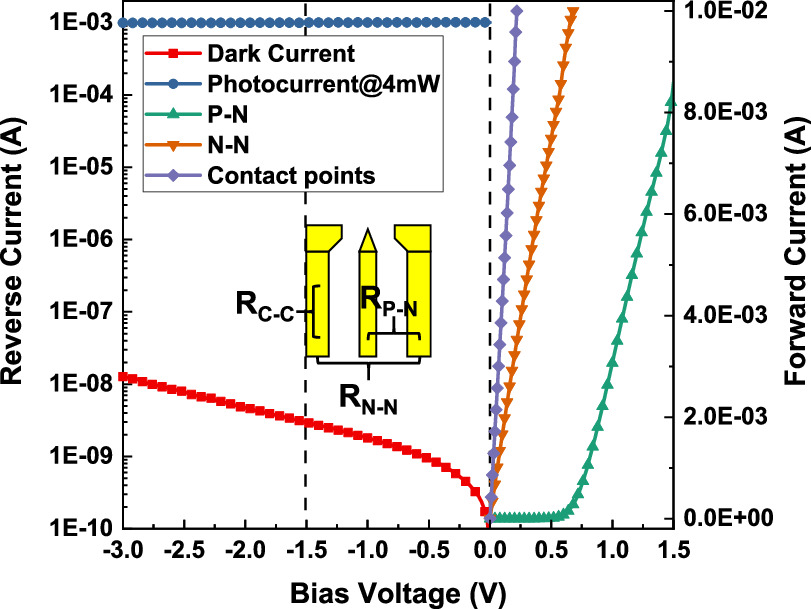
Fig. 2. I–V measurement results of the waveguide PD.
Download figure:
Standard image High-resolution image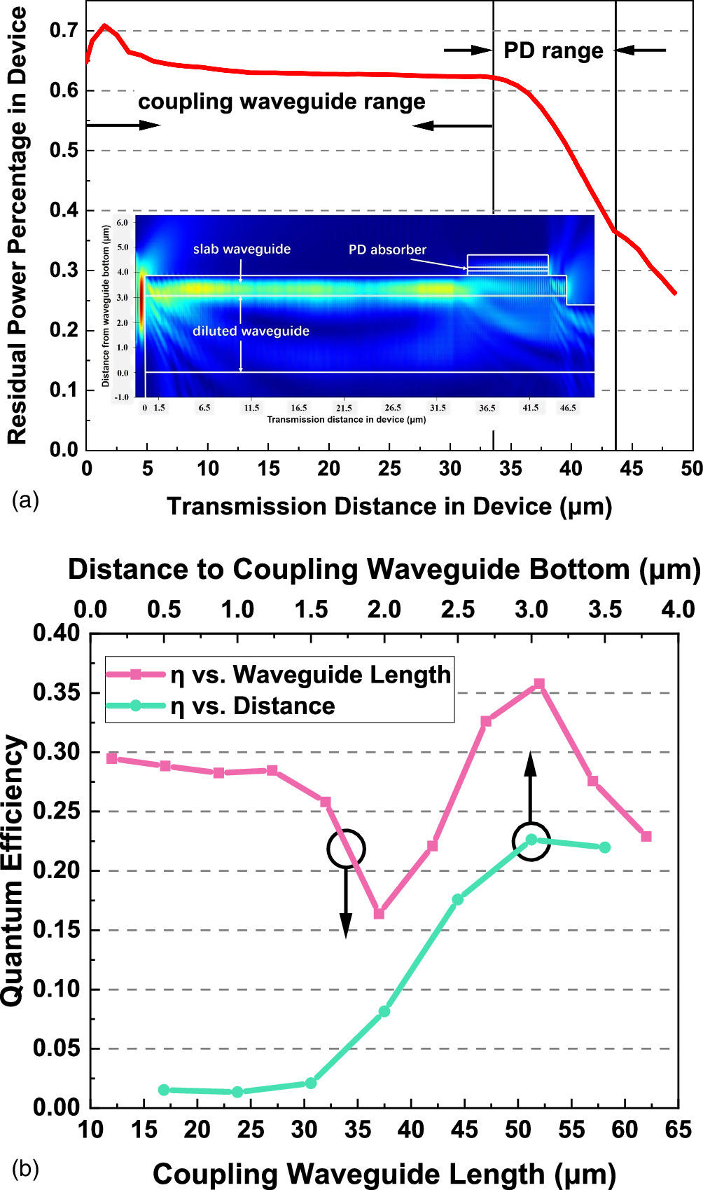
Fig. 3. (a) Residual optical power simulation result during transmission in the PD (inset: cross section of wave electric field vector distribution). (b) Quantum efficiency simulation results of 5 × 10 μm2 PDs with different coupling waveguide lengths and source center distances to the coupling waveguide bottom.
Download figure:
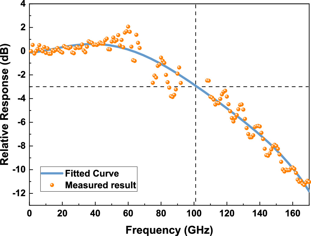
Standard image High-resolution imageThe frequency response of the waveguide PD is measured by microwave power-meters, with the intensity modulated input optical power realized by beating two narrow-band lasers near 1550 nm. Ground–signal–ground probes are used for on-chip contact, with internal T-biases for microwave power transfer to power-meters. The probe within 67 GHz is coaxially connected to the power-meter, while those beyond are connected by integrated metal waveguide tubes. Bandwidth results are illustrated in Fig. 4, under an average 4.5 mA photocurrent. The measured result has been calibrated by subtraction of extra losses besides the chip, which includes microwave losses from probes, T-biases, sensor heads of the power-meter, and electrical transfer lines. The fitted curve indicates a high −3 dB bandwidth over 100 GHz at −1.5 V.

Fig. 4. Bandwidth measurement results of the waveguide PD.
Download figure:
Standard image High-resolution imageTheoretical PD bandwidth is determined by both the carrier transit-time and the resistance-capacitance (RC) time. In the modified UTC-PD, the former is affected by the slower carrier within the structure. Relevant parameters are the near-neutral absorber thickness  which is esteemed as undepleted, the depleted absorber thickness
  and the other depleted regions' aggregate thickness
  , including the collector layer and the grading layers. To determine each parameter, electric fields inside the device are numerically calculated and plotted in Fig. 5. As can be seen, the absorber is divided into two parts, where a 70 nm near-neutral region (0.41–0.48 μm) stays almost constant in very low intensity while another 90 nm depleted region varies in intensity as the bias voltage increases. It reveals that a 40 nm lightly P-doped region of the 110 nm gradual P-type absorber has been depleted besides the 50 nm slightly N-doped absorber. Different field slopes are also obvious among the grading layers, the cliff layer and the rest of the n−-collector regions, adding to a total
  of 210 nm.
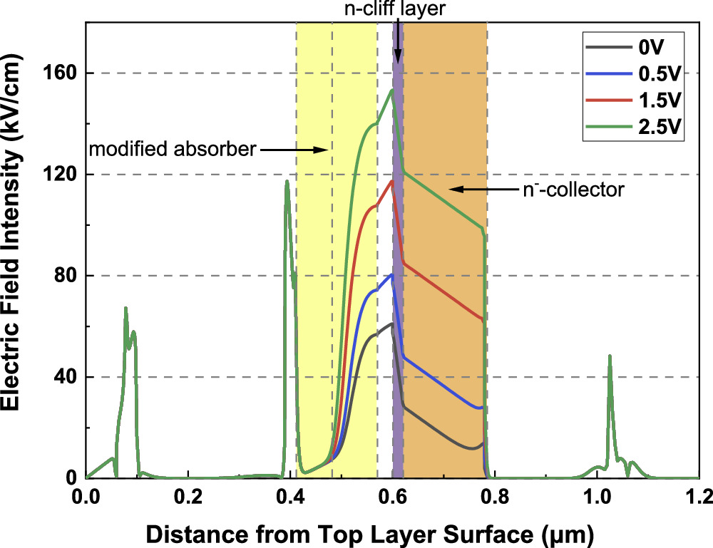
Fig. 5. Electric field simulation results for the PD.
Download figure:
Standard image High-resolution imageThe electron transit time  is estimated by the sum of the diffusion time
  in
in  thermionic emission time
  at the grading layer band-gap, and the drift time
  in
in  22)
22)

where  denotes electron diffusivity in the InGaAs absorber,
  the thermionic emission velocity, and
  , the electron overshoot velocity in the InP collector. The hole drift time
  is simply estimated by
  where
where  denotes the hole saturation velocity in InGaAs. The calculated
  of 1.8 ps is slightly larger than
  of 1.41 ps, yet the hole transit-time limited bandwidth of 310 GHz by
  23) is much larger than the measured bandwidth, indicating that the RC time should be the limiting factor. Parameters used for the estimation are summarized in Table II.
22,24–26)
23) is much larger than the measured bandwidth, indicating that the RC time should be the limiting factor. Parameters used for the estimation are summarized in Table II.
22,24–26)
Table II. Parameters for the bandwidth estimation.
| Parameters | Value |
|---|---|
| Wan | 70 nm |
| Wad | 90 nm |
| Wd | 210 nm |

| 130 cm2 s−1 |

| 2.5 × 107 cm s−1 |

| 3.0 × 107 cm s−1 |

| 5.0 × 106 cm s−1 |

| 13.9 |

| 12.6 |


| 50 μm2 |

| 1614 cm2V−1·s−1 |

| 140 cm2 V−1·s−1 |

| 8.5 μm |

| 0.31 μm |

| 7.7 μm2 |
A series capacitance including both  and
and  are considered:

where  denotes the absolute dielectric constant,
  and
and  , the relative dielectric constants for InGaAs absorber and InP collector, respectively, and
  the PD ridge area. The estimated
  of 19.122fF leads to a maximum RC-limited bandwidth of 166 GHz by
  where
where  is the standard 50Ω load resistance and the series resistance
  has been assumed to be zero.
23) Even this overestimated
has been assumed to be zero.
23) Even this overestimated  is much lower than
I–V curves are collected by two DC probes of the P-N CPLs, the two N-contact pads besides the PD, and the two contact points on the same signal line under forward bias, as shown in the inset in Fig. 2. Correspondingly, an  of 95.238Ω, an
  of 68.306Ω, and an
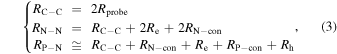
  of 22.381Ω could be deduced from the linear slopes of these curves. The resistances could be further decomposed:
where  denotes the probe-line contact resistance,
  the electron lateral transport resistance in the N-contact layer,
  the hole vertical transport resistance through the electron barrier layer,
  and
and  the semi-metal contact resistances of the N- and P-contact layers, all are illustrated in Fig. 6. Theoretical
  and
and  could be further approximated by:

where  denotes electron/hole mobility,
  the donor/acceptor doping density,
  the transport length,
  the carrier transport flow area (
 =
=  ), and
  the basic charge. Therefore, an
  of 11.19Ω, an
  of 14.23Ω, an
  of 0.92Ω, an
  of 8.73Ω, and an
  of 48.97Ω are calculated in sequence. The P-contact resistance is obviously higher than the N-contact due to an 82.27% smaller contact area. The deduced contact resistivity, however, is about 2.46 × 10⁻⁵ Ωcm2 and identical for both contacts.

Fig. 6. Estimated capacitance and resistances in measurement.
Download figure:
Standard image High-resolution image
To further reduce the RC time, both resistance and capacitance should be minimized, which requires a practical lower contact resistivity at 10−6 Ωcm2 and a shrunken PD ridge area. 27) However, the PD area needs to be optimized carefully considering the possible outcome of higher optical coupling loss and lower responsivity. More efficient methods, such as impedance-matched circuits and induced peaking, will be studied in the future. Regardless, the waveguide PD of 100 GHz may provide some prospective chip choice for the upcoming ultra-high optical transmission networks.
Acknowledgments
This work is supported by the National Key Research and Development Program of China (2020YFB1805701) and National Natural Science Foundation of China (61934003).