

Abstract
Conditions for the direct nitridation of the 4H-SiC(0001) surface by H2/N2 treatment and resulting surface structure were investigated by Fourier transform infrared spectroscopy (FTIR), X-ray photoelectron spectroscopy (XPS) and low-energy electron diffraction (LEED). The FTIR analysis probed both Si–H stretching vibration with back-bond containing N atoms and Si–N stretching vibration on the nitrided surface, while XPS analysis revealed the formation of an NSi3 structure with N density of ∼1 × 1015 cm−2. The LEED pattern for the H2/N2 treated surface exhibited a ( ×
×  )R30° superstructure. The results indicate that H2/N2 treatment produces a highly ordered H-terminated nitrided surface.
Export citation and abstract BibTeX RIS
Silicon carbide (SiC)-based metal-oxide-semiconductor field effect transistors (MOSFETs) have the potential to realize high-voltage blocking and low-loss conduction performances.1) Although the practical use of SiC-MOSFETs in voltage classes from 600 to 3300 V has already started in certain applications, enhancing channel mobility and stabilizing MOS interface characteristics are priorities to improve device performance and reliability. In terms of chip-integration, which allows for increased current density per area, trench-type MOSFETs with SiC(1-100) m-face or SiC(11-20) a-face as channel faces are now increasingly spotlighted.2) The development of SiC-insulated gate bipolar transistors with very high blocking voltages exceeding 10 kV is also expected for ultra-high-voltage applications such as power electronics equipment for power transmission/distribution system.
Typical SiO2/SiC interfaces contain higher densities of carrier traps and/or scattering centers than well-prepared SiO2/Si interfaces and tremendous trials have been made to improve carrier transport near the SiO2/SiC interfaces.3–6) Post-oxidation annealing in N-containing gas, i.e. NO or N2O, has been used to reduce the SiO2/SiC interface states and thus enhance channel mobilities.7–10) The local structure near N atoms on oxide and SiC(0001) interfaces has been studied using several techniques, such as X-ray photoelectron spectroscopy (XPS), low-energy electron diffraction (LEED), and X-ray photoelectron diffraction (XPD). It is revealed that each of the N atoms bonds to three Si atoms at the oxynitride interlayer formed on the SiC(0001) surface.11,12) More recently, the local atomic arrangement of the nitrided SiC(1-100) surface was studied by XPD, which suggested that the surface comprised Si- and C-facets and most N atoms substituted C sites at the topmost layer.13,14) A highly ordered nitrided surface like this is expected to pave the way to make an MOS interface by depositing a gate insulator.15)
In this study, we attempted direct nitridation of the SiC(0001) surface by H2/N2 treatment and investigated the structure of the nitrided surface.
Epilayers were grown on commercial 4°-off 4H-SiC(0001) substrates using a CVD reactor.16) After dicing to dimensions of 24 × 14 mm, the samples were cleaned using the RCA method beforehand and loaded into a high-temperature furnace. For H2 treatment, the samples were annealed in a Pd-filtered H2 gas flow for 15 min, a process diagram of which is shown in Fig. 1(a). The H2/N2 treatment comprised initial H2 treatment, followed by continuous annealing in a mixed H2/N2 gas flow for 15 min as shown in Fig. 1(b). The flow rate of H2 gas for H2 treatment was 50 slm (l min−1 at 0 °C, 1 atm). During the H2/N2 treatment, the flow rates of H2 and N2 were 10 and 1 slm, respectively.
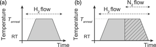
Fig. 1. Process diagrams of (a) H2 and (b) H2/N2 treatments.
Download figure:
Standard image High-resolution imageThe local structures, chemical compositions and surface morphologies were examined using FTIR (Thermo Fisher Scientific, Nicolet), XPS (ULVAC PHI, Quantum 2000), LEED (OCI Vacuum Microengineering, BDL800IR) and AFM (Asylum research). When measuring FTIR, incident polarized IR light created multiple attenuated total reflections (ATRs) between the sample and a Ge prism (1 mm thick), while two pieces of samples were clamped with a 4°-off c-axis kept perpendicular to the contact face of the prism.17,18) The direction of the incident light was parallel to [11-20], thus the electric field of the light was normal and parallel to the SiC(0001) surface in p- and s-polarization, respectively. The background and SiC bulk component were subtracted from the raw FTIR spectra. The LEED patterns were obtained at an electron energy of 100 eV and with no additional heating after applying H2 or H2/N2 treatment followed by air exposure and sample loading.
Figure 2(a) shows polarized-FTIR spectra of samples following H2 or H2/N2 treatment. Sharp absorption peaks were observed at 2128 cm−1 after H2 treatment and 2202 cm−1 after H2/N2 treatment in p-polarized spectra, respectively, but absent in s-polarized spectra, attributable to the monohydride Si–H stretching vibration. The narrow peak widths of 6 and 3 cm−1 respectively for H2 treated (1300 °C) and H2/N2 treated (1500 °C) samples indicate that Si–H monohydride structures are highly ordered. Monohydride Si–H stretching vibration was reportedly observed at 2128–2135 cm−1 for Si bonded with three C atoms (–CCC),17,19–21) with a corresponding peak (2128 cm−1) observed after H2 treatment as shown in Fig. 2(a). The possible origin of twin peaks has been reported due to the different SiC stacking arrangement under Si–H bonds.20) The frequency of Si–H stretching vibration is known to shift toward a higher frequency with the sum of atom electronegativities back bonded to the Si.17,22) The frequencies of monohydride Si–H stretching vibrations with different back-bond including C and N atoms, are calculated by adopting the approach previously reported.17) For Si bonded with (i) three C atoms (–CCC), (ii) one N atom and two C atoms (–NCC), (iii) two N atoms and one C atom (–NNC) and (iv) three N atoms (–NNN), the relevant figures are calculated as 2135 ± 13, 2159 ± 13, 2184 ± 13 and 2210 ± 13, respectively. The relative difference in the peak wavenumbers of absorption peaks observed after H2 and H2/N2 treatment is 74 cm−1 (=2202–2128 cm−1), which correlates well to the calculated value of 75 cm−1 (=2210–2135 cm−1) for Si–H stretching vibration with a back-bond containing three N atoms (–NNN). Since the width of the Si–H peak in the spectrum (1500 °C) is 3 cm−1, which is nearly half the frequency difference (6 cm−1) between Si–H (–CCC) twin peaks in the spectrum after H2 treatment, it is expected that one side of the Si layer, i.e. the hexagonal (h) or cubic (k) layer, will predominate on the surface after H2/N2 treatment.
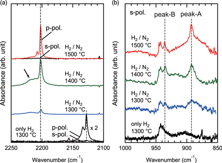
Fig. 2. (Color online) Polarized-FTIR spectra of 4H-SiC(0001) after H2 or H2/N2 treatment at various temperature. (a) Spectra around Si–H stretching vibration peaks. (b) s-polarized spectra around Si–N stretching vibration peaks. An arrow in (a) indicates a broad peak corresponding to the Si–H stretching vibration with back-bond containing O atom partially.
Download figure:
Standard image High-resolution imageThe s-polarized spectra in a range from 850 to 1000 cm−1 taken for samples after H2 or H2/N2 treatment at different temperature are shown in Fig. 2(b). After H2/N2 treatment, additional peaks were detected at 893 (peak-A) and 936 (peak-B) cm−1, which then intensified and narrowed with increasing treatment temperature. The peak frequency correlates well to the vibration of the Si–N antisymmetric stretching mode of the local structure NSi3 in Si3N4 crystal and amorphous silicon nitride.23–25) Splitting of the Si–N stretching mode to peak-A and -B could be attributable to that the hexagonal structure of underlying 4H-SiC would lead the local structure of near surface NSi3 not showing three-fold symmetry but slightly differing Si–N bond lengths.
The XPS spectra near Si 2p, C 1s, N 1s and O 1s signals for the H2 or H2/N2 treated surfaces are shown in Fig. 3. The area densities of each content were estimated by normalizing Si 2p intensities.26) The N 1s peaks were clearly observed after H2/N2 treatment, although under the detection limit when H2 treatment was performed. The binding energy (398 eV) of the main component of N 1s implies that each N atom is bonded to three silicon atoms, in line with previous reports.14,27) The N density was estimated as ∼ 1 × 1015 cm−2 (∼1 ML) for all samples, regardless of treatment temperature and significantly exceeding the reported values ∼2–5 × 1014 cm−2 for the SiO2/SiC interface treated by NO.28,29) Note that nitridation and oxidation processes occur simultaneously in NO treatment since NO decomposes and forms N2 and O2 at high temperature. Incorporated N atoms are removed with oxidation related to the O2 partial pressure, resulting in the saturation value.29) In contrast, there is no restriction in H2/N2 treatment, which can introduce N atoms with a density over the saturation value for the NO treatment.30)
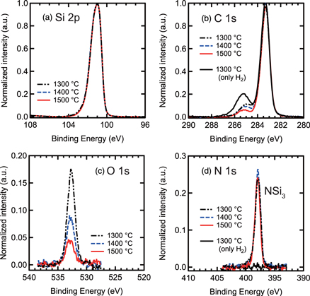
Fig. 3. (Color online) (a) Si 2p, (b) C 1s, (c) O 1s and (d) N 1s photoelectron spectra from surface after H2 or H2/N2 treatment at different temperatures.
Download figure:
Standard image High-resolution imageThe single component of O 1s peak (533 eV) mainly originates from the formation of Si–O bonds and the intensity decreased with increasing H2/N2 treatment temperature, indicating that removal of the oxidized layer on 4H-SiC was promoted or oxidation of the surfaces by residual oxygen in the furnace was suppressed at a higher temperature. This may correspond to the broad FTIR peak [as indicated by an arrow in Fig. 2(a)], which was observed for samples treated by H2/N2 at 1300 °C–1400 °C and which almost disappeared at 1500 °C, since a peak shift of Si–H stretching vibration toward a higher wavenumber is expected when inserting O atoms with larger electronegativity than N atoms in Si back-bonds. The estimated O density was 3 × 1014 cm−2 on the H2/N2 treated surface at 1500 °C, the ratio of O and N densities was ∼0.2 from the XPS results, reflecting how the surface Si atoms mainly bond to N and H atoms. Extensively low shoulder peaks of Si 2p, originating from the formation of SiOx, also underline the scarcity of Si–O bonds near the H2/N2 treated surface, which the estimated Si densities from the shoulder peaks were almost matched to the O densities estimated from the O 1s peak.
In addition, the shoulder peak of C 1s attributable to C–H and C–C bonds, which are considered absorbed after ambient exposure, was remarkably suppressed after H2/N2 treatment compared to H2 treatment alone. It has been reported that graphene can form on a SiC(0001) surface when annealing in UHV or ambient argon (Ar), revealing a clear peak of C–C bond at 285 eV.31) However, no such peak indicating the formation of graphene or C-rich layer was observed from samples treated in ambient H2/N2.
As shown in Figs. 4(a) and 4(b), a (1 × 1) LEED pattern was observed after H2 treatment at 1300 °C, although a ( ×
×  )R30° pattern appeared after H2/N2 treatment at 1500 °C. Shirasawa et al. reported the formation of a silicon oxynitride (SiON) layer with a (
 ×
×  )R30° structure following H2/N2 treatment at 1350 °C.11,12) Mizuno et al. also report the O-terminated nitrided surface with a (
 ×
×  )R30° structure formed on Si-poor surface by exposing to NO at 950 °C.30) In our H2/N2 treatment at a higher temperature range of 1400 °C–1500 °C, conversely, a very low density of O atoms and Si–O bonds on the surface, the formation of monohydride Si–H bonds with three N atoms in the back-bonds of each Si atom and the NSi3 with ∼1 ML amount of N atoms were observed concurrently. These findings suggest that an oxidized layer and Si–O bonds terminating nitrided layer were mostly removed or did not form significantly during our H2/N2 treatment at 1400 °C–1500 °C, i.e. by reducing O2 partial pressure and increasing temperature. Taken account of the fact that the surface exhibits the (
 ×
×  )R30° pattern, by substituting the top layer containing O atoms in previous reports for H atoms, a possible structural model for an H-terminated nitrided surface obtained by H2/N2 treatment is depicted in Fig. 4(c); topmost: H, second: Si, third: N, fourth: Si. We note that only the structural model for k-layer termination is schematically illustrated, although k- and h- termination layers possibly appear on the surface as mentioned before. Further detailed structural analysis is requested to verify the structural model presented here.

Fig. 4. (Color online) LEED patterns of SiC(0001) surfaces after (a) H2 treatment at 1300 °C and (b) H2/N2 treatment at 1500 °C. (c) Ball-stick model of the surface structure obtained by H2/N2 treatment.
Download figure:
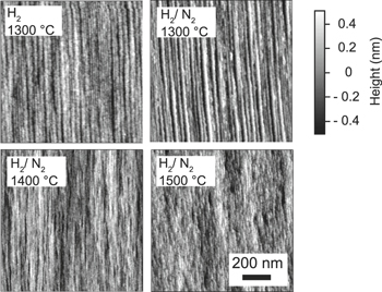
Standard image High-resolution imageThe AFM images taken for the H2 treated surface (1300 °C) and H2/N2 treated surface (1300 °C–1500 °C) are shown in Fig. 5. Unlike the surface-exhibited macro step-bunching after H2 or H2/N2 treatment at 1300 °C, it became rather smoother with fine steps when H2/N2 treatment was performed at 1400 °C–1500 °C. Also noteworthy was the fact that H2/N2 treatment at 1550 °C or higher weakened the FTIR Si–H and Si–N peaks and roughened the surface (not shown). Judging from both FTIR spectra and AFM images, the optimal temperature range for H2/N2 treatment can be considered 1400 °C–1500 °C under the present process conditions. Besides, ATR-FTIR analysis will be useful for monitoring nitrided SiC surfaces and optimizing the nitridation process.
Fig. 5. (Color online) Surface morphologies of the SiC(0001) surface after H2 or H2/N2 treatment at 1300 °C–1500 °C.
Download figure:
Standard image High-resolution image
In summary, we investigated direct nitridation on a 4H-SiC(0001) surface by H2/N2 treatment. The ATR-FTIR spectra indicate that the present H2/N2 treatment at 1400 °C–1500 °C provides a highly ordered H-terminated nitrided surface. The H-terminated nitrided surface includes the local structures of the NSi3 and monohydride Si–H (–NNN) at the same time; exhibiting a ( ×
×  )R30° structure. Because the present result only applies for an Si-face surface, further studies on the C-face are warranted as part of efforts to optimize the nitridation process for trench-type MOSFETs with the m-face as the channel face.