
Abstract
We present a study of the light output power and the thermal impedance of 281 nm emission AlGaN based micropixel LEDs. A modular interconnected micropixel array design is presented which enables dense packing with area and power scalability. We study 5–15 μm diameter stand-alone devices and parallel-connected micropixel arrays with 5 μm interpixel gaps. A standalone 5 μm pixel emits 291 W cm−2 at 10.2 kA cm−2 DC-drive. A power as high as 23 mW (361 W cm−2) was measured at a pulsed-pump current of 800 mA (∼15 kA cm−2) for an interconnected array. These are the smallest and brightest DUV LEDs to date.
Export citation and abstract BibTeX RIS
The consumer demand for point-of-use purification and disinfection has been tremendous since the emergence of the novel coronavirus (COVID-19) and its deactivation with DUV light. 1) AlGaN DUV LED's are the key to these important air–water purification and germicidal applications. Currently, mercury-based sources dominate the market for systems requiring high DUV radiation doses. Their use in applications such as face-mask disinfection and ventilation systems is problematic due to mercury toxicity. 2)
Since our early report of milliwatt-power AlGaN DUV LEDs, the last two decades have seen intense development to improve their performance. 3–6) Despite this, the reported external quantum efficiency (EQE) and wall-plug efficiency for AlGaN DUV LEDs are well below their visible counterparts. 7,8) This is primarily due to low light extraction efficiency (LEE) and thermal issues which are reduced but not eliminated even in flip-chip LEDs. 9,10) The junction heating of AlGaN DUV LEDs leads to efficiency-droop, early power saturation, and reduced device lifetime. 11–13) A key contribution to device self-heating is from its series resistance, which consists of contributions from the contacts, lateral spreading, and the vertical epilayer resistances. For DUV LEDs, the Ultra-Wide Bandgap (UWBG) AlGaN (3.43–6.0 eV) also dictates a high operating voltage. Although progress has been made in increasing the doping efficiency, 14–16) the large ionization energy of the p-dopant acceptors results in lower free hole concentrations for UWBG AlGaN, leading to higher contact and epilayer resistances. Furthermore, the thermal conductivity of ternary AlGaN layers constituting DUV LEDs is lower than that for the binary layers of the visible LEDs. 17)
The current spreading and series resistance issues in DUV LEDs were first addressed by our group using a 10 × 10 array of interconnected micropixel LEDs. 18–20) For that work, we used 25 μm diameter pixels with an interpixel gap of 15 μm where the interconnected n-ohmic contact, which blanketed the area surrounding all individual micropixels was placed. We showed that the interconnected micropixel design increases the light output power (LOP), reduces the series resistance, increases the device reliability, and largely eliminates current crowding. Gong et al. then published a study of the size-dependent opto-thermal properties of 400 nm emission InGaN single pixel LEDs. 21) They found the maximum power density (brightness), spectral stability and thermal properties to improve as the pixel size reduced from 300 to 20 μm. This was due to an increased ratio of the device sidewall surface-area and the mesa volume which facilitated efficient sidewall assisted out-radiation of the generated heat. 22) A similar trend was also observed by Ploch et al. for quaternary InAlGaN micro-LED arrays (λemission = 305–325 nm), where, the size limit (∼10 μm) was defined by an onset of saturation of the thermal resistance. 23) They concluded that further pixel size reduction would likely reduce the opto-thermal performance due to increased leakage currents at the mesa perimeters.
To date, no such studies of size-dependent LOP, nor thermal impedance have been reported for AlGaN DUV micro-LEDs. In this report, we present such a systematic study of individual and interconnected AlGaN MQW micropixel DUV LEDs with pixel sizes from 5 to 15 μm. We also explore a new interconnected micropixel design, which enabled high brightness and high power DUV emission. For this new design, the blanket n-contact network between the individual micropixels was removed to increase the active area coverage and reduce the optical absorption. 24) The n-contact for this present work forms a narrow picture frame border around a densely packed subarray of interconnected micropixels. The subarray interconnection process also passivates the pixel sidewalls and spreads the self-generated heat away from the individual micropixels, while avoiding current crowding. Then, multiple subarrays are interconnected [Fig. 1(a)]. This completed device is suitable for subsequent electroplating and flip-chip packaging. All the micropixel arrays of this study with different micropixel diameters have a total junction area of (6.36 × 10⁻⁵ cm2), which is also the same as of a reference, 90 μm diameter standalone LED.
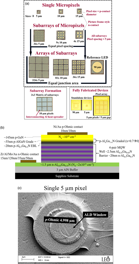
Fig. 1. (Color online) (a) Device layout and interconnection process overview with micrographs at each level of fabrication. (b) Structural details for the DUV LEDs of this study can be seen from the cross-sectional schematic. (c) SEM image of a single 5 μm pixel (defined by the p-contact diameter) with the Al heat-spreader.
Download figure:
Standard image High-resolution imageThe epilayer structure was grown over 3 μm thick thermally conductive AlN templates over c-plane sapphire substrates using metalorganic chemical vapor deposition. 25,26) The device structure and the epilayer growth details are shown in Fig. 1(b). The device fabrication procedure consisted of first using a Cl2/Ar chemistry inductively coupled plasma reactive ion etching (ICP-RIE) to define the micropixels and access the n-contact making n+-Al0.65Ga0.35N layer. Annealing in a nitrogen environment was then performed at 750 °C to activate the Mg-dopants. Then a narrow picture frame n-contact (5 μm wide) was fabricated around single pixels (for standalone devices) and the subarrays of pixels (for interconnected devices). The n-contact metal stack Zr(150 Å)/Al(1200 Å)/Mo(350 Å)/Au(500 Å) was deposited via e-beam and annealed at 950 °C for 3 min in forming gas by rapid thermal annealing (RTA). The internal dimension of this n-contact border was for all cases < 100 μm. Our past study indicates that this geometry precludes current crowding. 27) From the n-contact TLM measurements, the sheet resistance for the epilayer structure and the contact resistance were Rsh=120 Ω/□ and ρc = 6 × 10⁻⁴ Ω·cm2. Following the n-contact, Ni/Au p-contacts were formed over the individual micropixels and annealed at 500 °C for 5 min on a hotplate in an O2 environment. The p-metal dimensions were 5, 10 and 15 μm diameter for the micropixels.
The first micropixel interconnection stage began with atomic layer deposition (ALD) of a conformal 75 nm thick Al2O3 film. Windows above the p-contact regions of the individual micropixels were then opened by ICP-RIE with a high-power Cl2/BCl3/Ar based etch. This was followed with photoresist masking and electron-beam deposition of a 300 nm thick reflective aluminum heat-spreader to interconnect the individual micropixels thereby forming the subarrays. The Al interconnect blanketed the entire internal area of the n-ohmic picture frame borders. An SEM image of a fabricated micropixel with a p-ohmic diameter of 5 μm and the Al heat-spreader is shown in Fig. 1(c). The second stage of interconnection started with plasma enhanced chemical vapor deposited SiO2 (400 nm) followed by a SF6/CF3H/Ar dry-etching with RIE to open windows for each of the subarrays. For each mesa diameter, nine subarrays (of micropixels) were then interconnected to form LEDs with the same emission area as the reference 90 μm diameter single pixel LED. The final metal stack deposition blanketed and interconnected the 3 × 3 arrays of subarrays. Table I summarizes details for the various device geometries schematically shown in Fig. 1(a).
Table I. Relevant parameters for the devices of this study. S.S.A/V is the ratio of sidewall surface area to the mesa volume.
| Pixel/gap size | Junction area (single pixel) | Pixels per subarray | Pixels per array | Junction area (array) | S.S.A./V |
|---|---|---|---|---|---|
| 90 μm | 6.36 × 10⁻⁵ cm2 | Reference for Interconnected Arrays | 0.0417 | ||
| 15/5 μm | 1.77 × 10⁻⁶ cm2 | 4 | 36 | 6.36 × 10⁻⁵ cm2 | 0.2 |
| 10/5 μm | 7.85 × 10⁻⁷ cm2 | 9 | 81 | 6.36 × 10⁻⁵ cm2 | 0.27 |
| 5/5 μm | 1.96 × 10⁻⁷ cm2 | 36 | 324 | 6.36 × 10⁻⁵ cm2 | 0.44 |
Both standalone micropixels and the 3 × 3 arrays of interconnected micropixel subarrays were then measured and compared to the reference LED for their current–voltage–light output (I–V–L) and external quantum efficiency (EQE). A Si-photodiode and a calibrated photometer were used for the measurements. Using a thermal-driven spectral shift approach, 28) the junction temperature versus input electrical power was measured for the micropixel arrays and the reference LED.
All the measurements were made on-wafer. The pulsed measurements, for the micropixel arrays and the reference LED, were conducted using 500 ns wide pulses at 0.05% duty cycle to minimize device heating. Figure 2(a) shows the electroluminescence (EL) spectra of a single 5 μm pixel with the Al heat-spreader. The EL emission obtained at 2 mA (10.2 kA cm−2) under continuous wave (CW) pumping has undergone a small redshift, indicating moderate device self-heating, which becomes more severe with increasing injection current. The junction area normalized I–V–L characteristics for the single pixel devices under CW-pump are plotted in Fig. 2(b). The light generation increases with pump-current until junction heating leads to efficiency droop. 21,29) The brightness peaked at 291 W cm−2 at 10.2 kA cm−2 for the single 5 μm pixel with the Al heat-spreader. This was nearly a factor of 30 higher than the reference LED. As the pixel size shrinks, less absolute injection current (and total input power) is required to reach the same current density. Despite the increasing series resistance with decreasing pixel size for individual micropixels, arising from the reduced conductive cross-sectional area of the epi-structure and the ohmic contacts, the total joule heating for a given current density decreases with decreasing pixel size enabling high current density operation.

Fig. 2. (Color online) (a) The measured electroluminescence spectra of a single 5 μm pixel with the on-wafer Al heat-spreader under various CW-pump currents. (b) Junction area normalized I–L characteristics for single micropixels and the reference LED under CW-pump. The inset shows the J–V characteristics for the same.
Download figure:
Standard image High-resolution imageIn Fig. 3(a) the I–V characteristics of the equal junction area micropixel arrays and reference LED are plotted. The operating voltage and series resistance for the micropixel arrays is less than that of the broad-mesa reference LED and decreases with decreasing pixel size due to the growing area of the n-contact with the increasing chip footprint required to make equal junction area devices. The junction area normalized brightness at low input powers was found to be identical for a single 5 μm pixel (without the Al heat-spreader) and an interconnected array of the same size micropixels. This indicates minimal optical loss from the interconnection process. From the I–L data of Fig. 3(b), the highest output powers (and brightness) of 3.2 mW (50 W cm−2) and 23 mW (361 W cm−2) were delivered by the interconnected array of 5 μm pixels under CW and pulsed-pumping respectively. This translates to a 5.25-fold (CW) and 15.2-fold (pulsed) increase in maximum LOP compared to the reference LED. The bare-chip peak EQE of ∼1.5% was extracted from the CW data of Fig. 3(b). Regardless of pixel size, a 13.5% increase in the peak EQE was measured for the micropixel arrays over the reference device. This indicates no impact from sidewall defects or leakage currents, even for pixel sizes as small as 5 μm, which may be attributed to the post mesa-formation annealing. 30) Our results suggest that unlike GaN/InGaN LEDs, 21,23) the ideal mesa size for optimal performance of AlGaN DUV micro-LEDs resides in the sub-10 μm regime. They also support the assertion that the substantially higher peak LOP over the reference LED was enabled by improved thermal management of the micropixel arrays. Our interconnected micropixel design in this study is therefore an attractive approach to overcome thermal droop, a critical limitation for high LOP in AlGaN DUV LEDs. Table II compares the peak brightness, LOP and EQE for several reported research and commercial DUV LEDs.
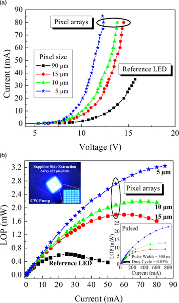
Fig. 3. (Color online) (a) I–V characteristics for the parallel-connected micropixel arrays and the reference LED. All of the devices have identical junction areas. (b) Absolute I–L under CW-pump for the equal junction area LEDs. The inset shows the pulsed mode output power for the same and the pulsing conditions. An image of a 6 × 6 subarray of 5 μm pixels and a 3 × 3 array comprised of such 6 × 6 subarrays of 5 μm pixels under CW-pumping is also shown. Over 95% of the pixels in the completed 3 × 3 array are working.
Download figure:
Standard image High-resolution imageTable II. Maximum brightness of several reported AlGaN DUV LEDs including flip-chip, tunnel-junction (TJ), nanopatterned sapphire substrates (NPSS), and state-of-the-art flip-chip multi-die encapsulated devices. SS denotes sapphire side light extraction and TS denotes top-side (p-electrode).
| Measurement | Junction area normalized LOP | Absolute LOP | EQE | |
|---|---|---|---|---|
| This work λ = 281 nm | On-wafer, SS | (CW) 291 W cm−2 | 0.057 mW @ 2 mA | 1.5% |
| (Standalone 5 μm pixel) | ||||
| This work | (CW) 50 W cm−2 | 3.2 mW @ 80 mA | 1.5% | |
| Interconnected array | On-wafer, SS | (Pulse) 361 W cm−2 | 23 mW @ 800 mA | |
| 324 × 5 μm Micropixels | ||||
| OSU 31) λ = 287 nm | On-wafer, TS | (CW) 54.4 W cm−2 | 0.49 mW @ 9 mA | 2.8% |
| (TJ, 30 μm × 30 μm) | ||||
| Peng, Dong 32) λ = 282 nm | On-wafer, SS | (CW) 4.5 W cm−2 | 6.56 mW @ 60 mA | 3.45% |
| (NPSS, Broad-mesa) | ||||
| Riken 33) λ = 282 nm | On-wafer, SS | (CW) 12 W cm−2 | 10.6 mW @ 250 mA | 1.2% |
| (Broad-mesa) | ||||
| SETI 34) λ = 275 nm | Flip-Chip (FC) | (Pulse) 32 W cm−2 | 80 mW @ 300 mA | 5% |
| (Broad-mesa) | ||||
| UV Craftory 3) λ = 285 nm | FC + Encapsulation | (CW) 6.0 W cm−2 | 475 mW @ 200 mA | N/A |
| (Broad-mesa) |
We next measured the junction temperature rise as a function of CW input power for the micropixel arrays and for the reference LED using the well-established electroluminescence spectral shift method (see Fig. 4). 10,21,23,28) Two sets of calibration measurements were carried out before device temperature quantification: (i) measurement of the redshift of the emission spectra with increasing junction temperature using a heated stage at a fixed pulsed pump-current; and, (ii) measurement of the blueshift of the emission spectra at room temperature with increasing pulsed pump-current. Both measurements were made using current pulses with a duration of 500 ns, a duty cycle of 0.05%, and a rest time of 10 min (between data points) to avoid pump-current induced device self-heating. The maximum redshift was 2.58 nm for a junction temperature range of 298–423 K. The largest observed blueshift of 0.782 nm was from an interconnected array of 5 μm pixels at an injection current of 50 mA. The mechanisms underlying the blueshift have been reported by multiple groups across several III-nitride platforms. 35–39) After the calibrations were performed, the device emission spectra was measured with increasing CW pump-current in a room temperature environment to estimate the junction temperature rise with input power. Then, for each pixel size, the spectral contribution of the current-dependent blue shift was subtracted from the junction temperature rise spectral data to remove its influence on the measurement. A linear fit was applied to the measured data in Fig. 4 to extract the thermal impedances. The steeper slope for the reference device, compared to those of the interconnected micropixel arrays, indicates significantly higher joule heating. The reduction in thermal impedance for the interconnected micropixel LED consisting of 5 μm pixels compared to the reference device was approximately 3.75-fold, supporting the origin of the substantially increased peak LOP to be thermal rather than optical. The linear fit in the inset underscores the strong dependence of thermal impedance on pixel size arising from the distribution of the input current through an increased number of micropixels and the increased sidewall out-radiation of self-generated heat. 22,23) The inset suggests that further reduction of pixel size is unlikely to significantly improve the on-wafer thermal performance.

Fig. 4. (Color online) Measured junction temperature rise as a function of CW input power for the equal junction area devices. A linear fit was used to extract the thermal impedances. The inset shows the linear relationship between measured thermal impedance and pixel size for all the equal junction area devices.
Download figure:
Standard image High-resolution image
In summary, we have presented a new design for the interconnected DUV micro-LED to enable densely packed scalable arrays of sub-20 μm diameter micropixels. We studied the light output and thermal properties of the devices and compared them to a reference LED with identical junction area. The reduction in pixel size down to 5 μm was shown to greatly reduce the thermal impedance of a micropixel array compared to a broad-mesa device. This is primarily from the reduction in device series resistance, a division of the input through an increased number of micropixels, and an increased sidewall out-radiation of the self-generated heat with decreasing pixel size. Due to the 3.75-times reduction in thermal impedance compared to the reference LED, the highest on-wafer output powers exceeding 360 W cm−2 were delivered by an interconnected array of 5 μm diameter micropixels. These are the smallest and the brightest reported DUV micropixel LEDs to date.
This research was supported by ARO contract W911NF-18-1-0029 monitored by Dr. M. Gerhold. Part of the AlN template work was supported by ONR MURI program monitored by Dr. Lynn Petersen and the DARPA DREAM contract (ONR N00014-18-1-2033), Program Manager Dr. Young-Kai Chen, monitored by Dr. Paul Maki. The characterization was partially supported the National Science Foundation (NSF), ECCS Award Nos. 1711322, 1810116, and 1831954.