
Abstract
We have investigated an interference experiment of the two-slit Young experiment using an improved self-alignment (SA) liquid crystal optical control device structure. The newly developed SA process and optimization of slit structure and slit width were redesigned to micron size in order to make the interference pattern clear. As a result, we observed a clear NOT logic operation where the center peak intensity of the incident light is inverted.
Export citation and abstract BibTeX RIS
1. Introduction
Organic electronic devices with advantages such as ultra-lightweight, ultra-thin, large-area capability, and flexibility have been used in organic LEDs (OLEDs) 1–3) and paper displays 4,5) organic thin-film transistors, 6–8) non-fullerene and copolymer-based solar cells, 9–11) organic–inorganic hybrid perovskite organic solar cells, 12,13) organic photodiodes, 14–16) pressure sensors, ECG/EMG, EEG, temperature, humidity, and gas/environment, 17–21) and RFID (RF Identification) tags, 22) and have been commercialized, 23) and OLED-based bio-sensing light sources have been developed. 24)
For electrooptic applications, liquid crystal (LC) devices have a half-century history of research and development, and liquid crystal displays (LCDs) are widely used for their merits of thinness, lightweight, low power consumption, and large-area productivity. 25,26) In addition, there are various applications using the birefringence of LCs. 27) These features are promising for optical computing applications of optical phase control. 28–32) If the ultimate optical control condition can be achieved under conditions where there is only one photon, then photon quantum computing could be also realized by introducing that photon into the optical path. Optical quantum computing can be applied to other optical quantum technologies, such as quantum sensors and quantum communications. 33) During these backgrounds, our group has studied basic research on the application of LC devices to Young's interference experiments using LC devices. 34) In that case, light from a light source is irradiated toward a screen at a short distance from a divided slit section; when light is divided by two slits, the light in the center is maximized where it should not be irradiated, and the intensity of the light is strengthened or weakened according to the optical path difference of the interference. In this time, we have studied the interference experiments of the two-slit Young's experiment using an improved self-alignment (SA) device structure, which has two major advantages: first, the slit itself can be used as a photomask, allowing automatic alignment of the slit and electrode; and second, the distance between the slit and the electrode can be made closer, thus reducing stray light. In addition, we have investigated the detailed patterns of interference fringes with the new SA LC-slit structure and the re-designed micron-width slit. This content was presented in an oral presentation PC-3 at the 9th International Symposium on Organic and Inorganic Electronic Materials and related Nanotechnologies, on June 8, 2023 in Kanazawa. 35)
2. Experimental methods
The process and experimental method for the SA electrode structure are investigated. In this experiment, a double slit with a = 35 μm slit width and d = 60 μm slit spacing was formed and diffraction patterns were evaluated. Here, to reduce stray light, we fabricated an LC device by applying the SA structure.
Figure 1 shows the device fabrication process. In the experimental process, Cr was first evaporated on the substrate using an electron beam evaporator, and patterning was done by photolithography to form a double-slit structure. Next, SiO2 was deposited by the sputtering method, followed by electron beam evaporation of indium-tin-oxide (ITO). Then, the negative photoresist (AZ-CTP100, Clariant) was spin-coated, and after pre-baking, a backside exposure method was carried out [Fig. 1(a)]. After developing with NMD-W (Tokyo Ohka Kogyo), a resist with a double-slit aperture was formed [Fig. 1(b)]. Next, ITO is etched with hydrochloric acid (17%) by adding Zn powder [Fig. 1(c)], and after the removal of the photoresist, the ITO is patterned using the SA patterning technique as follows; Cr is evaporated using an electron beam evaporator [Fig. 1(d)], and the slit width is adjusted by etching to fabricate a two-segmented electrode [Fig. 1(e)]. Compared to the previous report, this pattern shape was effective for clear peak generation and NOT operation because the slit and aperture could be well integrated, the number of insulators could be reduced, and the noise component could be reduced to about 1/4 of the previous experimental data. 36) As shown in Fig. 2, For the LC alignment layer, a 60° oblique evaporation method of SiO was used. The orientational direction was determined by changing a directional difference of 90° in the two regions. The substrates were evaporated two times using the photoresist coated on the alternate side of the regions, therefore, the orientation direction was symmetrical at ±45° from the center of the boundary. The ITO substrates coated on SiO 60° oblique evaporation were stuck together using a ball spacer of 6 μm diameter. Finally, LC material [LIXON-5049-XX, JNC, Δε = 5.1, Δn = 0.100, N(101 °C) Iso] was injected and sealed. The LC cell was fabricated, as shown in the upper figure of Fig. 3. The LC device characteristics are similar to the reflective type display mode (the 45-degree TN mode), 37) which has good polarization conversion and fast switching speed. To confirm the threshold voltage and operational behavior of the LC cells, the voltage transmittance (Tr-V) characteristics were measured under a polarization microscope.

Fig. 1. Device fabrication process under study. Here, a SA structure is formed in which the distance between the slit and LC is placed to the ideal limit.
Download figure:
Standard image High-resolution image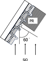
Fig. 2. The oblique evaporation method with divided into two different alignment regions. Alignment layer formation was patterned using a photoresist.
Download figure:
Standard image High-resolution image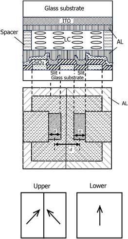
Fig. 3. Configuration of fabricated cell structure. The upper figure shows the exterior of the LC cell and the lower figure shows the oblique evaporation directions for the top and bottom substrates of the LC cell.
Download figure:
Standard image High-resolution imageNext, Young interference experiments using the fabricated LC cell were carried out using the measurement system, as shown in Fig. 4. The coordinate system is shown in Fig. 5. The slit width is a, the distance between slits is d, the Z for the distance to the screen, and x for the position on the screen. The intensity of the interference fringes on the screen is 38)

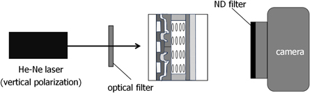
Fig. 4. Measurement system of Young's interference experiment. The light source under study is He-Ne laser light at a wavelength of 632.8 nm. The LC cell was placed at the center of the slit and the diffraction pattern of light after passing through the LC device was measured using the single-lens reflex camera with a neutral density filter.
Download figure:
Standard image High-resolution image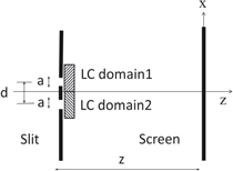
Fig. 5. Optical configuration with double slits. Configuration can be changed into two regions after passing through the slits. Here, d is the distance between two slits,  is the aperture length of the slit, Z is the distance between the slit and the screen, and x is the distance from the center of the screen.
Download figure:
Standard image High-resolution imageFor the interference measurement, the fabricated LC cell was irradiated with linearly polarized He-Ne laser light (wavelength of 632.8 nm). The laser light was diffracted at the double slit, and the applied voltage of the LC cell was varied to obtain the changes in interference fringes. An optical filter with a transmittance of 1.98% was used to reduce the light intensity. The voltage was changed between 0 and 9 V. Here, the voltage application method was changed in three ways: the voltage was applied (1) only to the right side of the split electrode, (2) only to the left side, and (3) on both sides. The voltage between 1.5 and 5.0 V, where the LC cell director is largely changed, was precisely changed by 0.1 V. Interference fringes were directly captured with a single-lens reflex camera with a neutral density filter. Light intensity was analyzed at eight-bit resolutions.
3. Results and discussion
3.1. Results
Figure 6 shows the Tr-V characteristics in one of the LC regions. The filled circles are for the parallel-Nicols case and the open circles are for the crossed-Nicols case. The threshold voltage is 1.3 V. It depends on the angle between the polarizer and the LC alignment direction, the maximum transmittance value for crossed Nicols at V = 0 is 0.624. By applying a voltage above 1.3 V, the transmittance increased once and reached a maximum voltage of 1.8 V and then gradually decreased above 1.8 V. The Tr-V curve is symmetrical with respect to half of the maximum transmittance values for parallel and crossed Nicols.
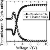
Fig. 6. Transmittance versus voltage characteristics at one of the LC region.
Download figure:
Standard image High-resolution imageFigure 7 shows the change in interference fringes when voltage was applied from the incident of the light side to the right electrode at (a) 0 V, (b) 1.5 V, (c) 1.8 V, (d) 2.4 V, (e) 4 V, and (f) 9 V. The He-Ne laser light is longitudinally polarized and the polarization angle is rotated 45 degrees from the LC orientation direction. The voltage is increased from 0 V, and the change in the interference fringes is observed around 1.5 V. By further increasing the voltage, a large change in the interference fringe is observed at 1.8 V. In this condition, the higher light intensity point became a very lower intensity, which is the highest peak intensity in the interference fringes at 0 V. In addition, a diffraction intensity change outside of the center was observed.
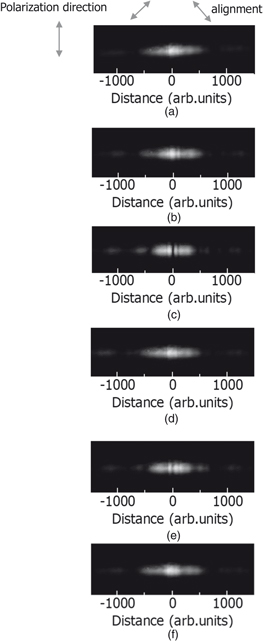
Fig. 7. Photograph of interference fringes patterns, where (a) 0 V, (b) 1.5 V, (c) 1.8 V, (d) 2.4 V, (e) 4 V, and (f) 9 V condition.
Download figure:
Standard image High-resolution imageIn order to observe numerical values of the interference fringes intensity from the photograph image, the intensity of the interference fringes was converted to the eight-bit gray level and analyzed, as shown in Fig. 8. The light intensity at 0 V, 1.8 V, and 9 V is shown in black, gray, and dotted lines, respectively. Figure 8 shows the case of V = 1.8 V, the center of the point, which is the highest intensity point, drops to an intensity close to zero. The center peak is clearly inverted between 0 V and 1.8 V. At 9 V, the center of the peak returns to the initial intensity at V = 0 V.
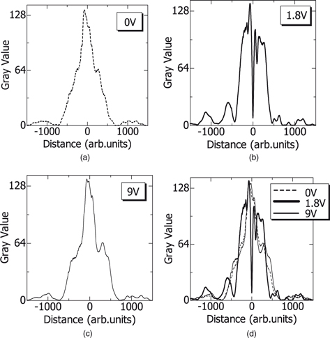
Fig. 8. Typical interference pattern with converted to eight bits grey level at horizontal line, where (a) 0 V, (b) 1.8 V, (c) 9 V, and (d) comparison among these conditions.
Download figure:
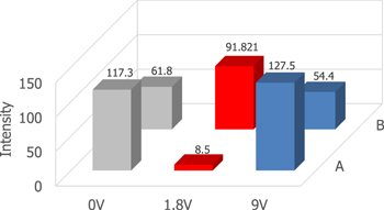
Standard image High-resolution imageFigure 9 shows the light intensity at points A and B, when V = 0 V, 1.8 V, and 9 V, respectively. Point A corresponds to the horizontal axis of distance = 0 and point B corresponds to the distance = 208. From this comparison, it can be clearly seen that the value of the intensity is reversed between points A and B. In addition, at point A, it could be observed a NOT logic operation where the intensity was exchanged to 0 and 1.
Fig. 9. Logic operation of position A and B for "0" and "1" points. Applied voltages are among 0, 2.5, and 9 V, where point A and B correspond to distance value at 0 and 208, respectively.
Download figure:
Standard image High-resolution image
3.2. Discussion
Before starting this series of experiments, the change in the center peak of the interference fringes could not be observed cleanly because of the large light intensity of the center peak and larger light noise. However, with the investigation of the experiment by reducing the light intensity and by controlling the interference fringes, a clear change in the center peak is observed. In detail, by applying the improved SA structure, and decreasing the slit width  diffraction by the slit appeared precisely and the amount of light in the direct beam became sharpened. Furthermore, the improvement of the device structure was reduced in the improved process, i.e. for example, reducing the number of insulators, which reduced the reflections generated by the insulators and eliminated stray light, compared to the previous literature.
36) This means that the diffraction pattern is modulated by the interference term of the cosine function by the double slit and the Fraunhofer diffraction.
39) This diffraction pattern is determined by
diffraction by the slit appeared precisely and the amount of light in the direct beam became sharpened. Furthermore, the improvement of the device structure was reduced in the improved process, i.e. for example, reducing the number of insulators, which reduced the reflections generated by the insulators and eliminated stray light, compared to the previous literature.
36) This means that the diffraction pattern is modulated by the interference term of the cosine function by the double slit and the Fraunhofer diffraction.
39) This diffraction pattern is determined by  and d. Therefore, the period of the cosine function and the sinc function were checked from Fig. 8, and there was a 1.78-fold difference between the two periods,
  = 35 μm and d = 60 μm. As a result, the cosine function due to the single slit is clearly observed, the light noise is reduced, and the NOT logic behavior could be observed. The intensity of the interference fringes became asymmetric at 1.8 V, where the NOT logic operation was observed. One possible reason is that applying voltage to the interference fringes causes a shift in the polarization direction of the diffracted light between the left and right slits, resulting in an asymmetry in the intensity of the interference light.
4. Conclusions
In this study, we investigated Young's interference experiments using the SA LC light control device. The use of the SA structure and improved device fabrication process could reduce the stray light, re-design the slit width to micron size, and divide the slit into trigonometric functions. This can improve the changes in the interference state and observation of the NOT logic operation. One of the issues of our experiment is reducing the stage fluctuation and vibration in environments. Further investigation is necessary to obtain the clear center part of the interference fringes. After that, Young's interference experiment using the SA LC light control device under single-photon conditions with micron-sized slits will be achieved in the future. At 1.8 V, the intensity of the interference fringes also became asymmetric. One possible reason is that applying voltage to the interference fringes causes a shift in the polarization direction of the diffracted light between the left and right slits, resulting in an asymmetry in the intensity of the interference light.
Acknowledgments
The work was supported by Scholarly Research Support from Toshiba Electron Devices & Storage Corp. This research is supported by the 2023 University of Toyama President's Discretionary Fund (Fund for the Revitalization of Education and Research).