
Abstract
In this study, we employed MBE to synthesize four MnSb samples on GaAs (111) B substrate at growth temperatures 300 °C, 400 °C, 500 °C, and 600 °C for GT-300, GT-400, GT-500, and GT-600 samples respectively. Surface morphology and elemental composition were characterized using scanning electron microscopy and energy-dispersive X-ray spectroscopy for four prepared samples. X-ray diffraction was performed to assess the crystal formation and surface quality of all samples. Epitaxial growth confirmation was performed using electron backscatter diffraction. Magnetic properties were assessed via superconducting quantum interference device measurements. Based on these comprehensive characterizations, the GT-500 sample, grown at a temperature of 500 °C (pyrometer 410 °C), demonstrated excellent surface morphology, crystal formation, surface quality, and magnetic properties. This sample holds outstanding potential for future applications, particularly in fabricating spintronics devices as a high-quality ferromagnetic source/drain, powering remote sensors, and thermoelectric devices.
Export citation and abstract BibTeX RIS
1. Introduction
Epitaxial growth is a crucial technique in semiconductor research and device fabrication. 1) By manipulating material features, epitaxial growth paves the way for developing electronic and spintronic devices. 1,2) In recent years, there has been a growing interest in exploring new materials and innovative growth techniques to tailor distinct material properties. 3,4) MnSb is a promising material for spintronic devices like spin valves and magnetic tunnel junctions due to its high Curie temperature and substantial spin polarisation. 5,6) Additionally, MnSb has been investigated for its thermoelectric properties, which involve converting heat into electricity or vice versa. 7,8) Thermoelectric materials like MnSb can be utilized in thermoelectric generators and cooling devices. 8,9) MBE has emerged as a powerful technique for precisely depositing thin films. 10)
MnSb is a manganese (Mn) and antimony (Sb) compound with magnetic and transport properties that make it desirable for device application. 11) Its ability to achieve spin-polarized transport and work well with existing semiconductor technologies makes it appealing. 12) By manipulating the epitaxial growth parameters of MnSb, its morphological state and magnetic properties can be altered. 13) Understanding the temperature-dependent aspects of MnSb epitaxial growth is significant for producing high-quality films with the intended crystal structure and properties. 14) The zinc-blende crystal structure of GaAs (111) B offers a close lattice match and a favorable surface orientation, which facilitates the growth of high-quality MnSb and MnAs films. 15,16) The (111) orientation of GaAs, which has a fcc crystal structure and exhibits a 3-fold rotational symmetry. 15) Conversely, the (0001) orientation of the ferromagnetic MnSb and MnAs exhibit a NiAs crystal structure and displays a 6-fold rotational symmetry. 17) The similarity in rotational symmetries between GaAs (111) and MnSb/MnAs (0001) enables a favourable epitaxial relationship between these materials. 17)
MnAs layers grown on GaAs (111) substrates, which have been extensively studied over the past few years, 18) but MnSb layers deposited on GaAs (111) B have not undergone in-depth investigation. Researchers have documented the structural and magneto-optical characteristics of MnSb layers grown on GaAs (110) and GaAs (001) substrates. 19) Additionally, they have explored the impact of GaAs (100) surface termination on the magnetic properties of MnSb layers. 19) Another study reported low-temperature growth and limited MnSb characterization. 20) P. J. Mousley and his research group have successfully grown MnSb (0001) on an InGaAs (111)A substrate. 21) Furthermore, a different research team recently reported their findings on the structural description and magnetic response of MnSb films deposited at cryogenic temperatures. 22) In parallel, other researchers have investigated the crystallographic orientation of primary and eutectic phases in a hypoeutectic Mn–Sb alloy. 23)
To the best of our knowledge, no report exists on the temperature-dependent epitaxial growth of MnSb on GaAs (111) B substrates using MBE with wide-range characterization. Additionally, this paper represents the first attempt to explore epitaxial MnSb growth through EBSD analysis. This research will contribute to the fundamental comprehension of MnSb epitaxial growth and pave the way for developing spintronic and thermoelectric devices.
2. Experimental methods
We used semi-insulating GaAs (111) B substrates with dimensions of 15 mm × 10 mm to carry out the growths. We cleaned it organically in acetone for 5 min, methanol for 5 min, and de-ionized water (DIW) for 5 min. Inorganic cleaning takes 10 min in semicoclean-23 produced by Furuuchi Chemical and 10 min in DIW, followed by organic cleaning. After thoroughly drying with N2, it was mounted on a molybdenum block by Indium (In), and then it was placed into a typical 3-chamber MBE system, which consists of loading, analysis, and growth chambers. After preheating the substrate in the analysis chamber to 370 °C, it was transported to the growth chamber. We synthesized MnSb at growth temperatures of 300 °C, 400 °C, 500 °C, and 600 °C (pyrometer readings were 219 °C, 317 °C, 410 °C, and 498 °C correspondingly) for GT-300, GT-400, GT-500, and GT-600 samples respectively. We aimed to retain the Sb and Mn beam equivalent pressure (BEP) ratio of ∼6, since this state was conducive to the MnSb growth system. 21) GaAs (111) B substrates were constantly subjected to an excess Sb environment with a 7.2 × 10⁻⁸ torr BEP. After removing the native oxide at ∼ 660 °C (pyrometer ∼590 °C), the following temperatures were changed to the growth temperature. To track the surface reconstruction of the samples, we performed an in situ Reflection high energy electron diffraction (RHEED) at 15 KV. It revealed a (1 × 1) pattern during surface reconstruction (Fig. 1). MnSb growth time was 90 min for each sample, while the BEP of Mn and Sb cells were 1.2 × 10⁻⁸ torr and 7.2 × 10⁻⁸ torr, respectively.
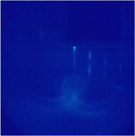
Fig. 1. Typical RHEED streaky patterns during thermal cleaning.
Download figure:
Standard image High-resolution imageFinding substantial information from RHEED observations during the growth of the four samples was challenging. We employed the Regulus 8230 system for detailed surface morphology research and surface composition. This system used scanning electron microscopy (SEM) and energy-dispersive X-ray spectroscopy (EDS) to analyze surface mapping and elemental composition. We used X'Pert PANalytical diffractometer at RT to clarify the crystal structure. To confirm detailed magnetic properties, we performed magnetization measurements at RT using a magnetic property measurement system (MPMS) equipped with a superconducting quantum interface device magnetometer. The applied magnetic field direction in MPMS was in-plane of the samples.
3. Results and discussions
3.1. SEM analysis and energy-dispersive EDS analysis
After completing the growths, we performed SEM of four samples (Fig. 2). Images of GT-300, GT-400, and GT-500 were captured in the same magnification, and the GT-600 was done in 1/10 low magnification. The surface of the GT-300 consisted of many white structures. GT-400 and GT-500 showed nearly similar surfaces. GT-600 sample was relatively different compared to other samples. On the surface of the GT-600, there were two distinct types of zones: dark and light areas in the SEM image. It has already been reported that the MBE growth of MnSb on various substrates tends to form some structures (nanoparticles). 24) The crystallites and different growth areas were found in all samples except the GT-600 samples. This type of growth was higher in the GT-300, suggesting that excess Sb can be captured and formed MnSb2, Mn2Sb3, and/or Sb. 25) All the major features were presented in the figure (Fig. 2) with atomic percentages. For the GT-300 sample, the atomic ratio of Mn and Sb contents on the film was near 1:5.
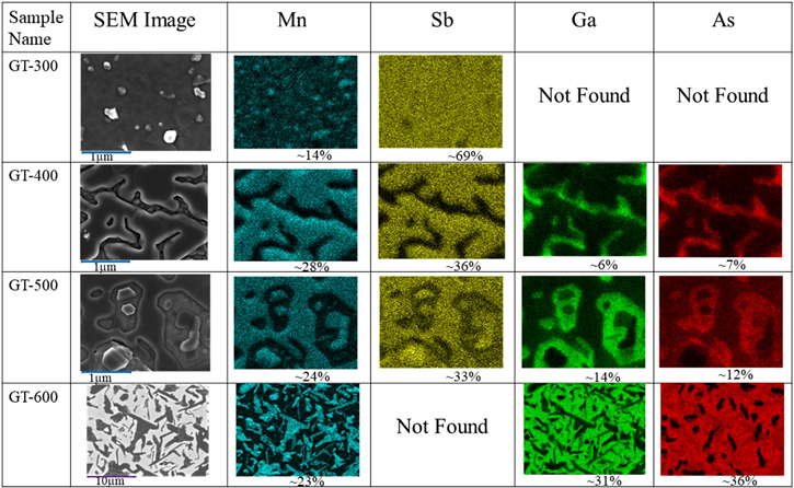
Fig. 2. (a) SEM image and EDS elemental maps of Mn, Sb, Ga, and As for GT-300, GT-400, GT-500, and GT-600 samples.
Download figure:
Standard image High-resolution imageIn the GT-300 sample, the whole surface was covered by Mn and Sb because there was neither Ga nor As in the EDS Mapping. For this reason, there was a strong possibility of forming MnSb as well as other compounds of Mn and Sb. 26) After analyzing the surface mapping of GT-400, Mn and Sb were deposited in almost the same regions and covered the whole smooth surface. This indicates that in the GT-400 sample, stoichiometric MnSb could be preferentially synthesized. In the GT-500 sample, the amount of Mn and Sb contents on film was nearly equal and almost similar to the GT-400 sample.
Among the four samples, the GT-600 sample did not show the presence of Sb. For this reason, this sample was not helpful for our targeted MnSb film. The stoichiometric ratio of Sb and Mn was excessively high in the GT-300 sample. In the case of GT-400 and GT-500 samples, there was a good balance of the Sb and Mn atomic percentage ratio. So, both can be potential candidates for the best MnSb film. Film thickness was measured using cross-sectional SEM and EDS images of the samples. We calculated the thickness as ∼188 nm, ∼105 nm, and ∼66 nm for the GT-300, GT-400, and GT-500 samples, respectively.
3.2. X-ray diffraction (XRD) pattern analysis
Figure 3 shows the 2Ɵ scanning result between 20° and 80° of GT-300 (Red), GT-400 (Blue), GT-500 (Green), and GT-600 (Black) samples. In all four samples, GaAs (111) and GaAs (222) peaks were observed at 27.30° and 56.35°, respectively. The lattice parameter of cubic GaAs was a ∼5.73 Å, which was close to the standard value. 27) In GT-300, GT-400, and GT-500 samples, MnSb formation was confirmed. A significant peak of (0002) MnSb was observed at 30.85° and (0004) MnSb at 64.29° (Fig. 3). It was a clear indication of hexagonal MnSb growth. Our extracted lattice parameter of hexagonal MnSb was c ∼ 5.79 Å. A similar result was also reported in a reputed journal. 25) In GT-300 samples, there were also many other significant signs for other materials such as (103) Mn2Sb, (201) Mn2Sb, and (223) Mn2Sb (Fig. 3). Similarly, GT-400 samples also showed two additional peaks at 51.85° for (222) GaMnSb as well as a weak peak for (201) Mn2Sb (Fig. 3). Analyzing the GT-500 pattern, one weak peak of (103) Mn2Sb (Fig. 3) was identified. All these results agreed with previously reported information. 25,28) Considering the above discussion, we can omit further characterization of GT-600 because there was no formation of MnSb. GT-300, GT-400, and GT-500 XRD patterns exhibited GaMnSb peak with lattice parameter 6.07 Å rather than GaSb (6.096 Å). 28) In our opinion, such a lowering of this lattice parameter indicated that the observed layer was instead a Ga1−x Mnx Sb zinc-blende solid solution phase with a high content of Mn. It has been reported that incorporating Mn into the GaSb lattice lowered the lattice constant. 29) Focusing on the GT-300 XRD pattern, the peak of (0002) MnSb was too weak and distorted. Additionally, (0004) MnSb peak was broadened with low intensity. So, the quality and the amount of MnSb crystal were inferior on the surface.
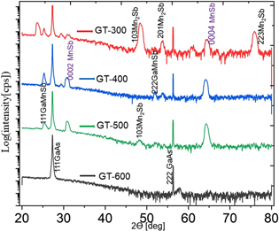
Fig. 3. XRD pattern of GT-300, GT-400, GT-500, and GT-600 samples.
Download figure:
Standard image High-resolution imageGT-400 and GT-500 samples showed better MnSb layer formation than GT-300 sample. The GT-400 sample showed a high-intensity peak of (111) GaMnSb compared to the GT-500 sample. Moreover, there was also a second peak of (222) GaMnSb in the GT-400 sample, but it was absent in the GT-500. The intensity of (0002) MnSb and (0004) MnSb of the GT-500 sample was better than the GT-400 sample.
3.3. Electron backscatter diffraction (EBSD) pattern analysis
EBSD was performed to confirm the epitaxial relationship. In the band contrast, which implies material difference, slightly dark regions correspond to smooth surfaces in the SEM image (Fig. 4). The phase color in EBSD, assuming NiAs-type hexagonal MnSb and zinc-blende-type cubic GaAs as constituent materials. It also perfectly corresponds with the band contrast and the EDS maps. Moreover, the inversed pole figure of the z direction (IPF Z) looks almost the same as the phase color (Fig. 4). That means the normal directions of MnSb and GaAs are along 〈0001〉 (red) and 〈111〉 (blue), respectively. It was consistent with the XRD result. Furthermore, IPF Y looks green in the whole area, and MnSb 〈12–10〉 was parallel to GaAs 〈101〉, which was similar to MnAs on GaAs (111) B. 18) IPF X indicates MnSb 〈01–10〉 was parallel to GaAs 〈112〉 (Fig. 4).
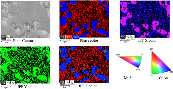
Fig. 4. EBSD images of GT-500.
Download figure:
Standard image High-resolution imageTherefore, we successfully confirmed the epitaxial growth of MnSb. To the best of our knowledge, this is the first report to confirm MnSb epitaxial growth on GaAs (111) B using EBSD. The sample's crystallographic orientation is crucial to generating distinct and apparent EBSD patterns. 30) A smoother sample surface may have aided in creating the EBSD pattern. Discussions suggest that the GT-500 sample had sufficient characteristics in each perspective to produce a well-developed EBSD pattern.
3.4. Magnetic properties analysis
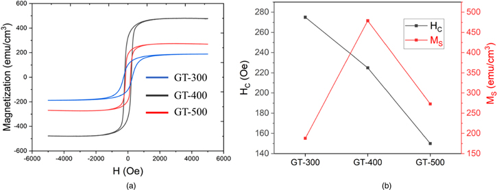
To determine the detailed magnetic properties of our samples, we conducted magnetization measurements at 300 K using MPMS. The magnetic field was applied along the in-plane direction of the samples. Figure 5(a) illustrates that ferromagnetic properties were observed in all samples. We estimated the volume of MnSb layers by considering the in-plane sample area and the epitaxial growth thickness. The saturation magnetization (Ms) and coercive fields (Hc) were extracted from Fig. 5(a) and plotted in Fig. 5(b).
Fig. 5. (a) RT M–H curve, and (b) saturation magnetization (Ms) and Coercive fields (Hc) of GT-300, GT-400, and GT-500 samples.
Download figure:
Standard image High-resolution image
Comparing the three samples, it was clear that GT-300 showed significantly degraded magnetic properties, such as a lower saturation magnetization and a larger coercive field. These can be due to the poor quality of the GT-300, like a relatively low atomic percentage of Mn in EDS and a relatively weak hexagonal MnSb peak in XRD. The high saturation magnetization of GT-400 is probably due to better filling of hexagonal MnSb on GaAs (from EDS). GT-500 exhibited the lowest coercive field because of the smoother surface morphology of hexagonal MnSb, which can promote spintronic application. 31) Furthermore, the smooth surface and well-formed crystal domain walls can swiftly propagate and reorient when subjected to an external magnetic field. 32) One research group reported the magnetic properties of MnSb, which was grown on a GaAs(100) substrate. 33) In their study, they observed a saturation magnetization (Ms) of 324 emu cm−3 and a coercivity of 264 Oe at a substrate temperature of 410 °C. Our experiment measured a saturation magnetization (Ms) of 479 emu cm−3 and a coercivity of 225 Oe at a substrate temperature of 400 °C [Fig. 5(b), GT-400]. Similarly, for a substrate temperature of 490 °C, they reported a saturation magnetization (Ms) of 267 emu cm−3 and a coercivity of 357 Oe. 33) On the other hand, our sample grown at 500 °C substrate temperature [Fig. 5(b), GT-500] exhibited a saturation magnetization (Ms) of 273 emu cm−3 and a coercivity of 150 Oe. Considering the findings mentioned above, our MnSb film demonstrated superior magnetic properties.
4. Conclusions
In this research, we successfully synthesized four MnSb samples on GaAs (111) B substrate using MBE at different growth temperatures. Our findings revealed that the GT-600 sample did not exhibit any evidence of MnSb formation on the substrate surface. Considering all the results, it can be concluded that the GT-500 sample, grown at a temperature of 500 °C (pyrometer 410 °C), showed remarkable properties for future applications. The synthesized GT-500 sample holds promise as a potential candidate for spintronic device fabrication, particularly in the role of a ferromagnetic source/drain. These findings contribute to our understanding of the epitaxial growth of MnSb films and emphasize the significance of optimizing growth temperature to attain the desired surface morphology and properties. Further research can focus on the precise growth temperature range between 400 °C and 500 °C and explore to fine-tune the epitaxial growth conditions. To further enhance its functionality, combining MnSb with a suitable semiconductor channel material has great potential. Incorporating InSb as the channel material and MnSb as the source/drain materials in spin-FET devices can leverage the unique properties of both materials.
Acknowledgments
This work was partially supported by research grant from Toshiba Electronic Devices and Storage Corporation.