
Abstract
Group III–V nitride semiconductors have been characterized by photothermal deflection spectroscopy (PDS) which can provide information on nonradiative recombination involving defect levels. After understanding the challenges of applying PDS to materials emitting light, the advantages and features of PDS are described for evaluating the defect level in the bandgap. The reciprocal of the slope of the PDS spectrum near the bandgap energy (Urbach-like energy) increases with increasing In composition in InGaN films. With an increase of the Urbach-like energy, the radial distribution determined by X-ray absorption fine-structure spectroscopy is likely to decrease. This may be attributed to the random aggregation of In atoms in InGaN films. Also, it is proposed that the Urbach-like energy may be considered for discussing the in-gap emission.
Export citation and abstract BibTeX RIS

Content from this work may be used under the terms of the Creative Commons Attribution 4.0 license. Any further distribution of this work must maintain attribution to the author(s) and the title of the work, journal citation and DOI.
1. Introduction
Defects due to dislocations, impurities, or vacancies in semiconductors affect physical properties and device characteristics. Therefore, intensive effort has been made to fabricate materials with few defects that exhibit good physical properties such as strong photoluminescence (PL) and high mobility. Group III–V nitride semiconductors for blue LEDs emit light well even with many dislocations (defects). 1) However, it is very important to study defects in the bandgap of III–V nitride semiconductors to improve performance in UV 2,3) and long-wavelength 4) LEDs, high-electron-mobility transistors, 5) and vertical power electronic devices. 6)
Group III–V nitride semiconductor materials are conventionally characterized by the FWHM of the rocking curve of X-ray diffraction (XRD). Better samples are often subjected to detailed defect evaluations. There are many methods for evaluating defects in semiconductor materials. Structural defects such as dislocations can be analyzed by the Burgers vector obtained by transmission electron microscopy. 7) Elements and their amount of impurities can be evaluated from the isotope ratio and intensity in secondary-ion mass spectroscopy. 8) Although N vacancies (VN) are difficult to detect, Ga vacancy type (VGa) defects are detected by positron annihilation spectroscopy. 9) These defects form the defect levels in the bandgap of the semiconductor, and their influence is reflected in the physical properties. For example, depending on the type and density of defects, the PL intensity and lifetime at the band edge change. 10) A deep defect level works as a path for leakage current, degrading device characteristics of photodiodes and transistors. Therefore, the measurement of the defect level and density in the bandgap can be a means of judging the quality of semiconductor materials and devices.
Deep-level transient spectroscopy (DLTS) is a well-known method for detecting deep defect levels up to ∼0.6 eV in the bandgap of Si. In III–V nitride semiconductors, DLTS can be applied to measure the defect levels formed at ∼1.0 eV from the bottom of the conduction band (Ec). 11) In order to detect the defect levels in the bandgap of group III–V nitrides more deeply, my research group applied photothermal deflection spectroscopy (PDS), 12) which was used for the defect characterization of hydrogenated amorphous Si (a-Si:H). This method does not require junctions such as p–n and Schottky barrier diodes using metal electrodes. It can estimate the absorption coefficient in the bandgap of semiconductors. Since defect characterization by PDS is not very familiar to researchers in the III–V nitride field, it is not well known what kinds of defects it can detect, and what kinds of capabilities it has.
In this paper, the potential of PDS is described for evaluating defect levels in the bandgap of III–V nitride semiconductors. While comparing it with other methods of characterizing defects in III–V nitride semiconductors, we will discuss the challenges we experienced while using the PDS technique. The correlation between the PDS spectra of InGaN films and the radial distribution of In–In/Ga atoms obtained from X-ray absorption fine-structure spectroscopy (XAFS) will be discussed with respect to the Urbach energy. Since PDS (a nonradiative process) is contrary to PL (a radiative process), the correlation between the emission related to the defect levels determined by PDS will be discussed. After describing the features and problems of PDS, we introduce interpretations of defect levels in the bandgap of III–V nitride semiconductors from both radiative (PL) and nonradiative (PDS) recombination processes.
2. Experimental methods
InGaN films with a thickness of 0.2–0.3 μm were grown on c-sapphire by horizontal metal–organic CVD (MOCVD) under atmospheric pressure. After growing a GaN layer (∼2 μm thick) for 1 h at 1000 °C on various substrates of c-sapphire, Si (111), or bulk GaN, the atmosphere inside the MOCVD reactor was changed from H2 to N2 for the InGaN film growth. An In0.03Ga0.97N film (0.1 μm thick) as an interlayer was grown at 830 °C for 30 min on the GaN film. Thick Inx Ga1−x N films were then grown at temperatures of 760 °C to 830 °C for 1 h under trimethylgallium, trimethylindium, and NH3 gas at a flow rate of 7 l min−1 using a constant In/(Ga+In) molar ratio of 0.95. The InN mole fraction was changed only by the growth temperature and was estimated from XRD of the films taking the strain effect into account.
In the PDS system used here, the sample surface was irradiated with monochromatic light from an ozone-free solar simulator Xe lamp (350–800 nm) as a pumping source at a normal angle with a chopping frequency of 11 Hz. The pumping light was focused through a cylindrical lens with dimensions of 1 × 10 mm2. A semiconductor laser (660 nm) as a probe was run on the sample surface in parallel, and the position of the probing laser was deflected according to the thermal energy converted from the nonradiative recombination of electrons excited by the pumping light. The details are described in Ref. 13.
XAFS measurements for the InGaN samples were carried out on the beamlines of BL01B1 at SPring-8. 14) The X-ray generated from the storage ring was monochromated by two Si (311) crystals and irradiated on the sample. Fluorescence X-rays of the In K-edge were obtained from the sample and detected using a 19-element Ge solid-state detector.
3. Results and discussion
3.1. Defect evaluation by DLTS and steady-state photocapacitance spectroscopy
Table I shows the characteristics of the methods used for evaluating the defect levels of III–V nitride semiconductors. Schottky or p–n junctions are always required for the methods of DLTS and steady-state photocapacitance spectroscopy 15) (SSPC). These techniques utilize the fact that the capacitance of the depletion layer changes transiently when the voltage applied to the junction is changed stepwise. When the n-type semiconductor contains defect levels that act as electron traps, a voltage in the forward direction (reducing the depletion layer) causes the levels in the bandgap to be occupied with electrons. When a reverse bias is then applied stepwise (widening the depletion layer), electrons are emitted into the conduction band. The electrons are ejected outside the depletion layer by the electric field applied to the depletion layer. As a result, the space charge density in the depletion layer changes transiently. The change in capacitance is measured at each temperature to obtain the defect energy level as the activation energy in DLTS. Although it depends on the detection sensitivity of the capacitance-measuring instrument, in the case of Si, a sample with a shallow donor density of 1015 cm−3 can be detected up to a defect level of 1010 cm−3. The defect level energy in GaN is usually evaluated at about 0.2 to 1.0 eV from Ec by measuring at temperatures of 77 K to 400 K. Although the detection area is limited to the depletion layer, it has the advantage of enabling one to evaluate defect density quantitatively.
Table I. List of defect evaluation methods for III–V nitride semiconductors.
| Method | DLTS | SSPC | PAS a) | PDS |
|---|---|---|---|---|
| Electrodes (junction) | Must (Schottky, p–n) | Must (Schottky, p–n) | not necessary | not necessary |
| Absolute estimation of defect density | Good (∼1011 cm−3) | Good (>1014 cm−3) | difficult | Possible |
| Detecting depth | Depletion layer | Depletion layer | Corresponding to abs. coeff. | Corresponding to abs. coeff. |
| Deep level from conduction band minimum | ∼1.0 eV | 0.7–4.0 eV | Around bandgap energy | 1.0–4.9 eV |
| Material properties | Require good electrical | Require good electrical | Not required | Not required |
a)Photothermal acoustic spectroscopy (see the next section).
In the measurement procedure of SSPC, a forward bias is applied so that the trap level in the depletion layer is occupied by electrons, the same as in DLTS. After applying a reverse bias, monochromatic light is irradiated to eject the trapped electrons, and the variation of capacitance caused by the light irradiation is measured at a constant temperature. 16) It is possible to detect between defect levels having an energy difference corresponding to the energy of the irradiated monochromatic light. GaN can be measured by DLTS at temperatures as high as 600 °C, so defect levels as deep as 1.5 eV can be detected. 17) On the other hand, in SSPC, the monochromatic light is irradiated to the sample, so the defect level in the bandgap of GaN up to the VB can be obtained at RT. It should be noted that unlike DLTS, it does not directly indicate the energy level from the bottom of Ec, but rather the energy difference between levels like PDS as mentioned below. In addition, it is necessary to arrange a measurement system such as depositing a transparent electrode for light irradiation or irradiating from a polished back surface. The detection limit of SSPC seems to be about 1014 to 1015 cm−3 from the measurement of highly insulative bulk GaN samples. 18)
Both DLTS and SSPC depend on the characteristics of Schottky and p–n junctions, and cannot measure electrically inactive materials. The hole density in GaN is low due to the relatively high activation energy of the Mg acceptor level in GaN. When a depletion layer is formed, the acceptor density reaches a high value of 1018 cm−3 or more. For this reason, it is difficult to form a good Schottky junction on p-GaN, and the leakage current becomes very large especially under reverse bias. The high background acceptor density significantly reduces the detection sensitivity for deep levels. For these reasons, DLTS measurements on p-GaN are difficult. Furthermore, since AlGaN and samples with wider bandgaps have highly insulative properties, it is difficult to measure defects electrically.
3.2. Features of PDS
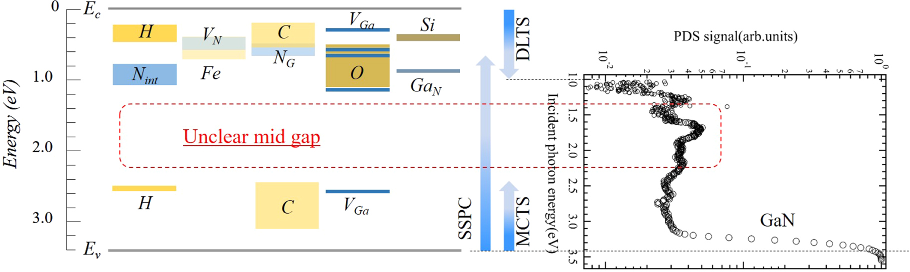
Figure 1 shows a schematic illustration arranged from Ref. 19 for the defect levels formed by VGa, VN, interstitial elements, and external factors (impurities) in the bandgap of GaN. The right side shows the spectrum of GaN obtained by PDS. With the bottom of the conduction band set to zero, the incident photon energy corresponding to the bandgap energy is adjusted to the value of the bandgap of GaN. (As will be described later, we believe that the PDS spectra of group III–V nitrides are observed in the VB side, similar to the SSPC spectra). Defect levels below the conduction band can be detected by DLTS. Defect levels above the VB are detected by minority carrier transient spectroscopy, 20) which measures capacitive transient response similar to DLTS by generating minority carriers with optical pulses above the bandgap.

Fig. 1. Illustration of defect levels caused by intrinsic factors and impurities in GaN modified from Ref. 19. The PDS spectrum of GaN is placed with the incident photon energy from the bottom of the conduction band in the right panel.
Download figure:
Standard image High-resolution imageDLTS and SSPC can cover defect levels in a wide range from the upper VB to the lower conduction band. However, information around 1.5 to 2.8 eV from Ec is limited. PDS may have the potential to access and detect defect levels in the midgap with high sensitivity, as shown in the typical n-GaN PDS spectrum. In addition, since the signal can be detected even if the semiconductor material is electrically insulative, it has the potential to evaluate both p-GaN and AlGaN. Photoacoustic spectroscopy, 21) in which heat generated by nonradiative recombination is detected by a microphone rather than by deflection of a probe laser as in PDS, has also been used for III–V nitrides. Although it is possible to detect signals at the band edge, it is currently difficult to detect signals in the bandgap.
3.3. Issues of PDS for III–V nitride semiconductors
PDS is a measurement method that utilizes the subtle deflection of a laser passing parallel to the sample surface due to the heat generated when electrons excited by monochromatic light recombine at nonradiative centers. Since the refractive index changes due to heat generation, the sample is placed in a liquid whose refractive index changes greatly with respect to heat. Since CCl4, commonly used in PDS measurements in a-Si:H, was found to etch the GaN surface, PDS measurements for III–V nitrides were carried out in Fluorinert instead of CCl4. By switching the light source between a Xe lamp and a halogen lamp, it is possible to measure from 1.0 eV to 4.9 eV. AlN can be evaluated by PDS if a light source with sufficient intensity at the wavelength of 200–250 nm is available.
PDS measurement for a-Si:H was used as a technique to characterize small absorption coefficients in the bandgap. 22) The PDS spectrum is obtained by integrating the density of states at the band edges and the defect states in the bandgap. The slope of the sharp intensity change near the band edge is attributed to the broadening of the Urbach edge due to compositional disorder. 23) This compositional disorder is defined as the reciprocal of the gradient and is an index of amorphous structural disorder like the Urbach energy. The defect levels in the bandgap are due to dangling bonds in the a-Si:H. The defect density can be estimated from the correlation with the intensity obtained by the method of ESR. 24,25) Based on these concepts, PDS was applied for evaluating the defects of III–V nitrides. Since PDS is originally a method for obtaining relative absorption coefficients, it cannot be used for materials in which some of the excited electrons recombine radiatively. 26) However, the light-emitting efficiency of GaN at RT is only a few percent, meaning that nonradiative recombination is dominant. This is why our group has used it to evaluate the defect levels of III–V nitrides. We have to pay attention to the defect evaluation of III–V nitride semiconductors by using PDS techniques after understanding that there are various issues as described below.
First, the problem is which side of the VB or the conduction band is reflected in the signal detected by PDS. In the case of a-Si:H, the PDS spectrum was considered to reflect the conduction band side. 22–26) The PDS spectra (especially the tail state near the bandgap energy) of InGaN films with different In compositions were similar to the VB spectra observed by hard X-ray photoemission spectroscopy (HAX-PES). 13) From this result, we believed that the PDS signal near the band edge was derived from the electronic state close to the VB side, although there was no method for measuring the conduction band in detail. Since the nonradiative recombination process at the top of the VB in light-emitting materials is not well understood, the reciprocal of the slope of the top of the VB of the PDS spectra obtained from III–V nitrides is defined as Urbach-like energy rather than the Urbach energy.
In order to obtain the absorption coefficient in the bandgap of a-Si:H, the PDS intensity at the bandgap energy was matched with the absorption coefficient determined by optical absorption. This was based on the condition that a-Si:H did not emit at the band edge. It is doubtful whether the absorption coefficient in the bandgap can be obtained for III–V nitrides using the same process as that for a-Si:H. Therefore, the PDS signal at the edge of the band has been normalized for comparison among III–V nitride samples. From our experience, a GaN sample with high defect density is likely to have large Urbach-like PDS signals in the bandgap. 18)
The next issue is sample thickness. For PDS measurement, the thickness of a-Si:H is typically 0.1 to 1 μm. Considering the absorption coefficient, the monochromatic light penetrates the entire film regardless of the wavelength. The thickness of the GaN sample is several micrometers for thin films and 400 μm or more for bulk GaN. Therefore, the penetration depth of the excited monochromatic light depends on the wavelength according to the absorption coefficient. As a result, the PDS signal intensity also depends on the depth. Defects existing from the substrate to the sample surface, such as threading dislocations, may enhance the PDS signal intensity. This problem will be remarkable if the defect distribution is larger in the depth of thickness. The detection region of DLTS and SSPC is the width of the depletion layer, and the probing region by the positron annihilation method is also limited to a depth of 1 μm. Although each method can obtain a quantitative defect density, it has its own problems in understanding defects in the entire sample.
As mentioned at the beginning of this section, in order to estimate the defect density of a-Si:H from the absorption coefficient in the bandgap of the PDS spectrum, the calibration curve was obtained through measuring the dangling bond density by ESR. Since almost one defect level was detected in the bandgap of a-Si:H, the correlation between the absorption coefficient and defect density was not so complicated. Since III–V nitrides have wide bandgaps, various peaks can be observed in the PDS spectrum as shown in Fig. 1. There is the problem that not only is each level not identified definitively, but also the nonradiative recombination caused by the energy difference between the levels is not clearly known. It is very difficult to identify the origin of defect levels and to estimate the absolute value of defect density. When the same sample of bulk GaN was evaluated by both PDS and SSPC, the PDS signal intensity qualitatively reflected the defect density. 18)
Finally, we describe a phenomenon peculiar to the PDS measurement of III–V nitride film samples. GaN film is grown on SiC and Si substrates in addition to sapphire substrates. Furthermore, heterostructures such as AlGaN/GaN and AlGaN/InGaN are formed for the fabrication of devices. When GaN thin films and heterostructures on substrates are evaluated by PDS, the signal from the layer with the smallest bandgap or the layer with the highest density of defects is preferentially detected. In a GaN thin film on a Si substrate, the VB spectrum of Si is detected by PDS for a longer wavelength. In addition, signals from GaN are preferentially detected even when evaluating wide-bandgap barrier layers of AlGaN/GaN or AlInGaN/GaN heterostructures. If the defect density in the bandgap of the underlying GaN is high in InGaN/GaN structures, the InGaN layer cannot be evaluated by PDS, though it has a lower bandgap. It is necessary to be careful with regard to the PDS signal origin for sample with several layers.
Although there are some problems in the evaluation of III–V nitrides by PDS as described above, ion-implanted GaN samples are considered to be the most suitable for PDS measurement. This is because the depth of ion implantation is limited and many defects are introduced so that it emits no light and is also electrically inactive. The crystalline improvement of the GaN region damaged by Mg ion implantation by thermal annealing is very important for generating p-type conduction in the application of III–V nitrides to electronic devices. The Urbach-like energy obtained by PDS clearly decreased, indicating structural improvement, 27) though XRD measurement was useless due to the influence of the underlying thicker GaN region. For this reason, PDS is particularly useful for defect level evaluation of ion-implanted III–V nitride semiconductors.
In addition to III–V nitrides, PDS was applied to wide-bandgap semiconductors such as Ga2O3 and NiO, 28) which are used in the hole transport layer of perovskite solar cells. Using the chemical stability of Fluorinert, we were able to obtain a correlation between the increase in mobility of the organic transistor and the improvement in Urbach energy. 29,30)
3.4. XAFS for InGaN films
When GaN bulks with quite low values of FWHM in XRD rocking curves were measured by PDS, the Urbach-like energy for some of them was ∼80 meV, 18) which was worse than that of a-Si:H. It is necessary to consider what the Urbach-like energy of III–V nitrides represents. We performed PDS and XAFS measurements of InGaN thin films with different In compositions, and compared the Urbach-like energy with the radial distribution.
Figure 2(a) shows the Fourier transform results (∣χ(R)∣) of k2(χ) for InGaN films grown on bulk GaN substrates, sapphire substrates, and Si (111) substrates. When compared to the reference InN results at the peak of 3.3 Å, the peak at the second-nearest neighbor (In-Ga/In) appears at 2.9 Å, a shorter radius reflecting the smaller lattice constant of InGaN. The amplitude of ∣χ(R)∣ indicated the coordination numbers of In atoms in the local structure. From the report of XAFS measurement using linearly polarized X-rays for Inx
Ga1–x
N quantum wells done by Miyanaga et al., the In atoms were randomly distributed in the horizontal direction but aggregated in the vertical direction.
31) The intensity of ∣χ(R)∣ for the vertical direction was lower than that for the horizontal one. Since the ∣χ(R)∣ for the InGaN on Si (111) was lower, the In atoms were likely to be aggregated in the local structure. The InGaN film on the GaN bulk substrate showed a value of the FWHM of the  reciprocal lattice less than 100 arcsec. On the other hand, it was 360 arcsec and 540 arcsec on the sapphire and on the Si substrate, respectively. One of the reasons for the lower intensity of ∣χ(R)∣ was considered to be the increased fluctuations in bond angles between atoms caused by the crystalline quality.
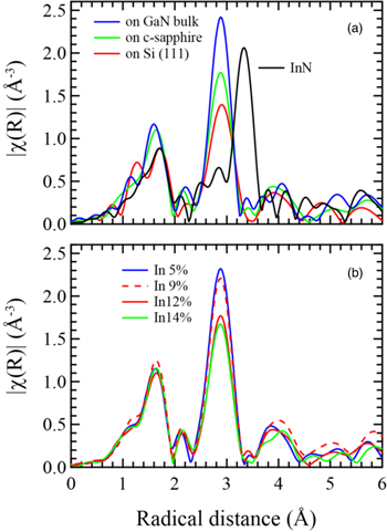
Fig. 2. Radical distribution determined by XAFS detecting the In K-edge for (a) InGaN films grown on various substrates, and (b) InGaN films with different InN mole fractions grown on sapphire substrates.
Download figure:
Standard image High-resolution imageFigure 2(b) shows the radial distributions of InGaN films with different In compositions on a sapphire substrate. In this range of InN mole fractions, the distance of the second-nearest neighbors was the same, but the intensity of the distribution decreased significantly when the In content exceeded 10%. The values of the Urbach-like energy of the Inx Ga1−x N films obtained from the PDS spectra gradually increased with increasing In content. 13) They were 112 meV and 48 meV for x = 0.12 and 0.05 in the Inx Ga1−x N film, respectively (no PDS measurement for x = 0.09 and 0.14 in Inx Ga1−x N). Similar to the case of GaN on a Si (111) substrate, the In atoms were aggregated in the local structure of Inx Ga1−x N films with InN mole fractions higher than about 10%. We supposed that this may be related to the N deficiency in the InGaN films due to the growth at lower temperatures. It seems that the N deficiency occurred at the same time as the aggregation of In atoms. The top of the VB of III–V nitrides is composed mainly of N 2p orbitals and is hybridized with group III elements. 32) We supposed that this might result in the increase of Urbach-like energy, which will be discussed in the next section.
3.5. PDS and PL for InGaN films
Figure 3 shows the PDS (red) and PL spectra (blue) of InGaN thin films with different In compositions, and the Tauc plot (yellow) converted from the UV–vis spectrophotometer. The GaN film sample shows a PL peak almost at the absorption edge [Fig. 3(a)]. For the In0.05Ga0.95N film, the slope of the PDS spectrum changes at around 3.1 eV, and a tail state is observed on the low-energy side [Fig. 3(b)]. For the In0.08Ga0.92N film, the strength of the tail state increases. The PL peak shifts to the energy where the slope of the PDS spectrum changes, and the energy difference between the PL peak and the absorption edge increases [Fig. 3(c)].
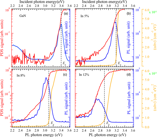
Fig. 3. PDS (red), PL (blue) and Tauc plot (green) for (a) GaN, (b) In0.05Ga0.95N, (c) In0.08Ga0.92N and (d) In0.12Ga0.88N films grown on GaN/sapphire substrates. Green lines show the Tauc plot evaluated from UV–vis absorption. α , h, and ν are the absorption coefficient, the Planck constant, and the photon frequency, respectively.
Download figure:
Standard image High-resolution imageThe decomposition efficiency of NH3 to generate N radially decreases with low-temperature growth. The low-temperature growth of the InGaN films caused the In composition and VN defects to increase. The VB top must be affected by VN. Recent theoretical calculations have reported that N vacancies are the most likely to form, and that this state forms over EV with +3 charge states. 33) It seems to correspond to the tail state detected from 3.0 eV to 2.4 eV in the PDS spectra with In composition of 5% and 8% in Fig. 3.
The binding energy of In 4d is lower than that of Ga 3d. 34) The VB spectra of the Inx Ga1–x N films observed by HAX-PES were shifted to lower binding energy with an increase of In composition, due to the In 5p orbital being hybridized with N 2p. The band offset between InN and GaN was about 1.5 eV. 35) As the In composition increased, the Urbach-like energy increased due to the larger aggregation of In atom arrangements. The change of slope in the PDS spectra in Figs. 3(b) and 3(c) might have been caused by both the tail state caused by VN and the shift of the hybridized In 5p + N 2p orbital. No slope change was observed in the PDS spectrum of Fig. 3(d) for the In0.12Ga0.88N film. This is because the VN states may have been covered by higher Urbach-like energy. Further increase of the In composition of the InGaN film with more than 50% of In caused an In adlayer to form on the surface which was detected below the conduction band. 35) PL might occur around VN with a +3 charge where the aggregation of In atoms may be locally high. Consequently, the difference between the absorption edge and the PL peak energy increased as the In composition increased.
3.6. PL–PDS correlation for GaN film thickness
Yellow luminescence (YL) was observed in PL from GaN [Fig. 3(a)], while no YL from InGaN films with higher Urbach-like energy was detected. It was thought that a sample which emitted no light such as YL related to defect levels in the bandgap (in-gap emission) would be good. Interestingly, no in-gap emission was observed from InGaN, which has a higher defect density than GaN. The in-gap emission from the ion-implanted sample induced by thermal annealing has been used as an indicator of structural recovery. 36) Therefore, it seems that the presence or absence of in-gap emission is not necessarily an indicator of the degree of defect density in the sample. Since PDS and PL are two sides of the same coin in terms of radiative and nonradiative recombination, we consider the emission intensity in the bandgap of GaN and the PDS signal intensity in this section.
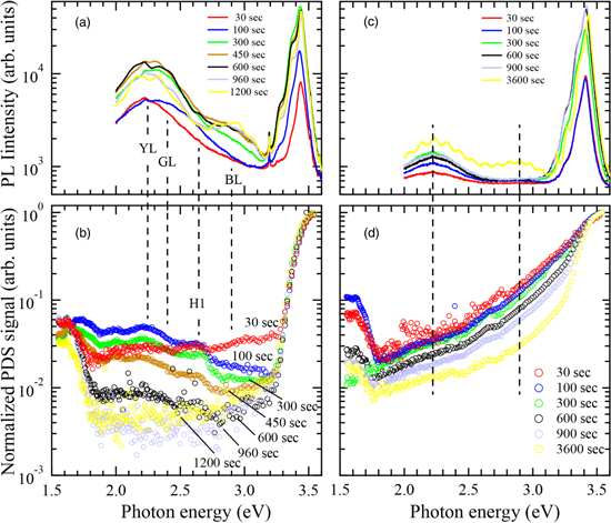
Figures 4(a) and 4(b) show the PL and PDS spectra of GaN thin films grown on AlN templates/sapphire substrates, and Figs. 4(c) and 4(d) show those of GaN grown on low-temperature GaN (LT-GaN) buffer layers on sapphire substrates. PL and PDS measurements of GaN films grown on each substrate for different times were performed. The intensities of the PL at the band edge were almost the same. The in-gap emission intensity is clearly stronger for the GaN films on AlN templates, and the PDS intensity in the bandgap is lower. Since the PDS intensity in the bandgap decreases as the film thickness increases, the PL intensity of YL and green luminescence increases. The peak intensity in the gap of the PDS spectrum and the energy position of the emission peak are almost the same. It can be interpreted that emission from inside the gap is observed because the nonradiative recombination of the level inside the gap is reduced.
Fig. 4. (a) PL and (b) PDS spectra for GaN films grown for various times on AlN templates on sapphire. (c) PL and (d) PDS spectra for GaN films grown on sapphire substrates using an LT-GaN buffer layer.
Download figure:
Standard image High-resolution image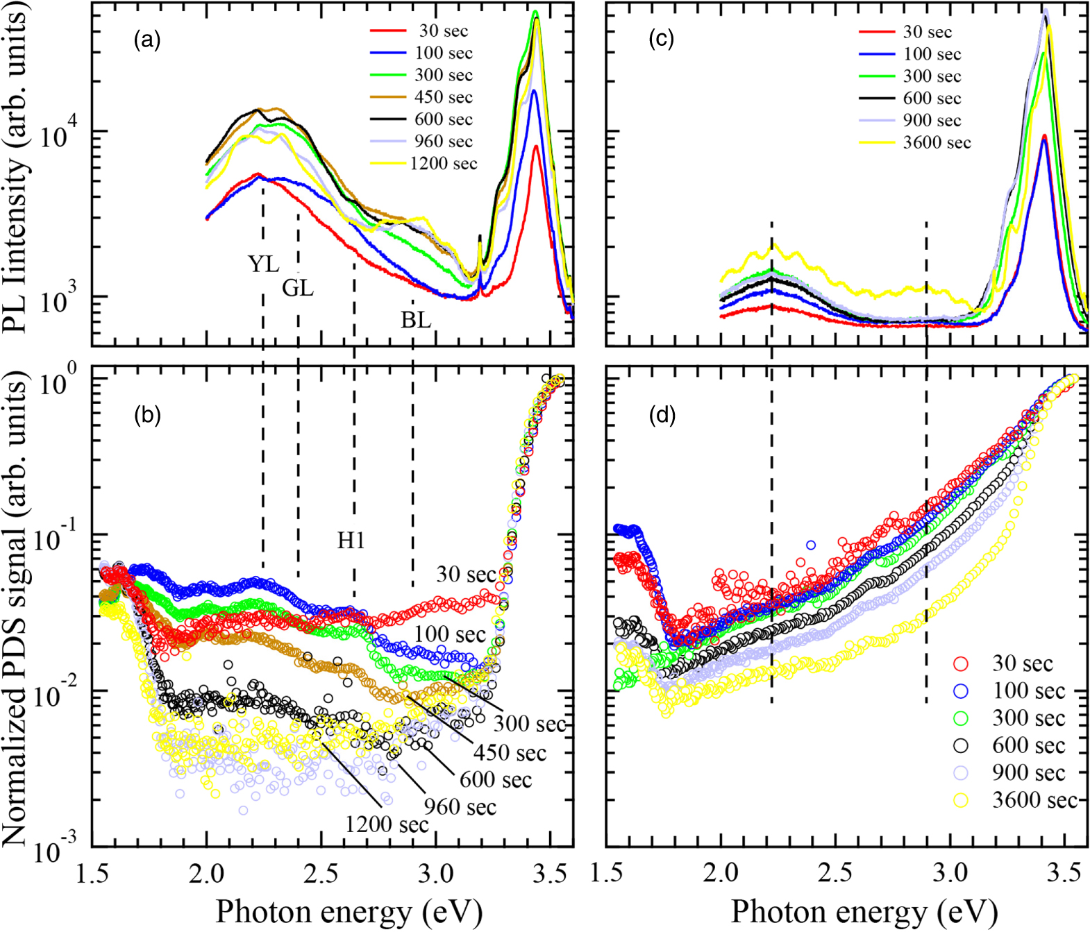
The Urbach-like energy of the PDS spectra of the GaN sample on an LT-GaN buffer layer was not improved with an increase of growth time (film thickness), as compared with that on an AlN template. This is the reason why the LT-GaN layer was so defective that the Urbach-like energy and defects in the bandgap were increased. Since the PDS method detects the most defective region as mentioned in Sect. 3.3, the PDS signal from the buffer layer had an influence on that from the GaN films for the growth time lasting until 900 s. For the PDS spectrum of GaN grown for 3600 s, the influence from the LT-GaN buffer layer was reduced and a clear Urbach-like energy was observed. The value was 91 meV which was much worse than that for the GaN films on the AlN template. The PDS signal intensity at 2.8 eV for the GaN film grown on an LT-GaN buffer layer for 3600 s decreased, and in-gap emission of blue luminescence was observed in the PL spectrum. Although the PDS intensity at 2.8 eV was comparable with that from the GaN grown on an AlN template for 300 s, the PL intensity was lower. Overall, the intensity of in-gap emission was weak for GaN films on the LT-GaN buffer with higher values of Urbach-like energy. When the crystalline quality of the ion-implanted sample was improved by thermal annealing, the Urbach-like energy was improved and in-gap emissions emerged. 37) Therefore, it seemed that the Urbach-like energy was related to the in-gap emission. Considering that the in-gap emission was caused by the band edge luminescence from the PLE measurement, 37) it was thought that the Urbach-like energy would be involved for electrons excited at the band edge to diffuse to the radiative recombination centers in the bandgap. For the current III–V nitride semiconductors in which defects exist, it seems necessary to consider the correlation between the Urbach-like energy and the in-gap emission.
4. Conclusions
This paper describes the characteristics and problems of evaluating III–V nitride semiconductors by PDS. The method of PDS has the feature of being able to detect the defect energy levels in the bandgap over a wide range from 1.0 eV to 4.9 eV without forming electrodes. The PDS method is available for electrically and optically inactive materials such as ion-implanted GaN and AlGaN with highly insulative properties. Considering the radial distribution determined by XAFS, we suppose that the higher Urbach-like energy and tail state near the band edge of the PDS spectrum of the InGaN film may be caused by the aggregation of In atomic arrangements and the N deficiency. From PDS (nonradiative) and PL (radiative) measurements for GaN films, it was suggested that the Urbach-like energy might be related to the emission from defect levels. It is expected that PDS characterization will be one of the useful tools for discussing defects in III–V nitrides.
Acknowledgments
The XAFS measurements were performed at BL01B1 in SPring-8 (proposal No. 2017B1428). The author thanks Dr. K. Saito of SPring-8 for supporting the XAFS experiment, and Prof. T. Honda of Kogakuin University for valuable discussions.