
Abstract
The development of a high-power EUV light source is very important in EUV lithography to overcome the stochastic effects for higher throughput and higher numerical aperture (NA) in the future. We have designed and studied a high-power EUV free-electron laser (FEL) based on energy-recovery linac (ERL) for future lithography. We show that the EUV-FEL light source has many advantages, such as extremely high EUV power without tin debris, upgradability to a Beyond EUV (BEUV) FEL, polarization controllability for high-NA lithography, low electricity consumption, and low construction and running costs per scanner, as compared to the laser-produced plasma source used for the present EUV lithography exposure tool. Furthermore, the demonstration of proof of concept (PoC) of the EUV-FEL is in progress using the IR-FEL in the Compact ERL (cERL) at the High Energy Accelerator Research Organization. In this paper, we present the EUV-FEL light source for future lithography and progress in the PoC of the EUV-FEL.
Export citation and abstract BibTeX RIS
1. Introduction
It is well known that the transistor number per chip has almost doubled every 2 years following Moore's law. The lithography resolution R is given by the light source wavelength λ, numerical aperture NA, and process parameter k1 as follows,

The light-source wavelength has become gradually shorter and shorter to keep Moore's law alive because the resolution is linearly proportional to the wavelength. The wavelength of EUV lithography is 13.5 nm, which is fitted to the reflectivity of Mo/Si multi-layer mirrors. In EUV lithography, high-volume manufacturing (HVM) started a few years ago using a 250 W laser-produced plasma (LPP) source. 1) In the LPP source, tin plasma generated by a CO2 drive laser and tin droplets provides intense EUV light for the scanner system with EUV optics. Contamination of tin debris to the collector mirror is one of the issues of this system. Another issue of EUV lithography is stochastic effects. 2) In EUV lithography, the absorbed photon number on a wafer is much less than those of the excimer lasers at the same dose because of the much higher photon energy. If the dose is insufficient, stochastic pattern defects appear on wafers. 3) High EUV power is needed for suppressing the stochastic effects at high throughput. The EUV power required for mitigating the stochastic effects was estimated for the maximum throughput of future scanners. 4) The estimated EUV power is more than 1.5 kW for the 3 nm node and 2.8 kW for the 2 nm node. Therefore, EUV lithography will require a more powerful EUV source in the future.
Free-electron lasers (FELs) 5) are roughly divided into two types, oscillator FELs, and self-amplified spontaneous emission (SASE) FELs. In an oscillator FEL, an electron beam from an electron accelerator emits light in an undulator, interacts with the undulator light stored in an oscillator, and amplifies the FEL light. However, the FEL wavelength is limited to longer than about 100 nm by poor mirror reflectivity for short-wavelength light. In an SASE-FEL, spontaneous emission from the high-quality electron beam provided by an accelerator is self-amplified in a long undulator without any oscillator and external seed. It is suitable for short wavelength FELs such as an EUV-FEL. Linear accelerators (linacs) used for SASE-FELs are also categorized into two, normal-conducting (NC) and super-conducting (SC) linacs. NC linacs are used for many FEL facilities such as LCLS, SACLA, FERMI, SwissFEL, PAL-XFEL, and so on, but the average current of the electron beam is limited to less than ∼100 nA to avoid the deformation of the linac cavity by high heat load. On the other hand, SC linacs have a much higher bunch repetition frequency and average current (typically a few 10 μA) because of extremely low heat load. They are operated in FLASH and European XFEL at present and will be used for LCLS-II and SHINE projects. The SC linacs are more suitable for high-power FELs.
ERLs (energy-recovery linacs) 6) are more powerful FEL drivers compared to ordinary linacs without the energy recovery described above. Figure 1 shows schematic views of an ordinary linac and an ERL. In an ordinary linac, the accelerated electron beam is dumped immediately after the FEL emission. On the other hand, in an ERL, the accelerated beam is returned to the main linac after the FEL emission by the recirculation loop, decelerated down to almost the injection energy for energy recovery, and then dumped. The low-energy beam from the injector and the high-energy beam from the recirculation loop alternately pass in the accelerating and decelerating RF phases of the main linac respectively. Therefore, the acceleration energy in the main linac is recovered, and the dumped beam power and activation are drastically reduced. As a result, a much higher bunch repetition frequency and average current (typically 0.1 ∼ 10 mA) are achieved in an ERL to provide much higher FEL power. There are several ERLs of 10 ∼ 160 MeV with FELs such as ERL-FEL at Jefferson Laboratory, Novosibirsk ERL at BINP, and ALICE at Daresbury Laboratory operated at present or in the past. For example, the ERL FEL at Jefferson Laboratory achieved more than 10 kW IR power by using an oscillator FEL. 7) An EUV-FEL based on ERL can be a most powerful EUV light source by using the energy recovery scheme and SC accelerator technology to overcome the current issues of EUV lithography.

Fig. 1. Schematic views of (a) an ordinary linac and (b) an ERL. In an ERL, the accelerated beam is returned to the main linac in a decelerating RF phase after the FEL emission to recover the acceleration energy and is dumped after deceleration down to the injection energy, while it is dumped without energy recovery immediately after the FEL emission in an ordinary linac.
Download figure:
Standard image High-resolution imageAn EUV-FEL light source based on ERL has been designed and studied for future lithography 8,9) and the design concept and future prospects of the EUV-FEL light source were clarified in the previous articles. In this progress review paper, after the overview of the EUV-FEL light source, advantageous features of the EUV-FEL light source are especially particularized to show differences from the LPP source clearly and comprehensively. The extremely high-power performance of the EUV-FEL light source is demonstrated by a new start-to-end simulation. The simulated EUV power is significantly higher than those of the previous articles. The conceptual design of key components in an optical beamline, where the intense FEL light is delivered from the EUV-FEL to multiple scanners, is explained. Furthermore, possible upgrade schemes to BEUV-FELs are proposed, and the simulated BEUV-FEL spectrum is compared to a measured reflectivity curve of the BEUV multi-layer mirror. It is also emphasized in this paper that polarization control of the FEL light is important to make the most of the polarization effects in high-NA lithography and can be realized by keeping high FEL gain and power by our proposed scheme. In addition, the estimated electric consumption and construction and running costs of the EUV-FEL light source are shown and compared to those of the LPP source. The proof of concept (PoC) of the EUV-FEL light source using the compact ERL (cERL) IR-FEL and significant progress in the demonstration of the PoC are also presented in this progress review paper. More recent progress toward future high-power FEL operation at the cERL is briefly described.
2. EUV-FEL light source for future lithography
2.1. Overview
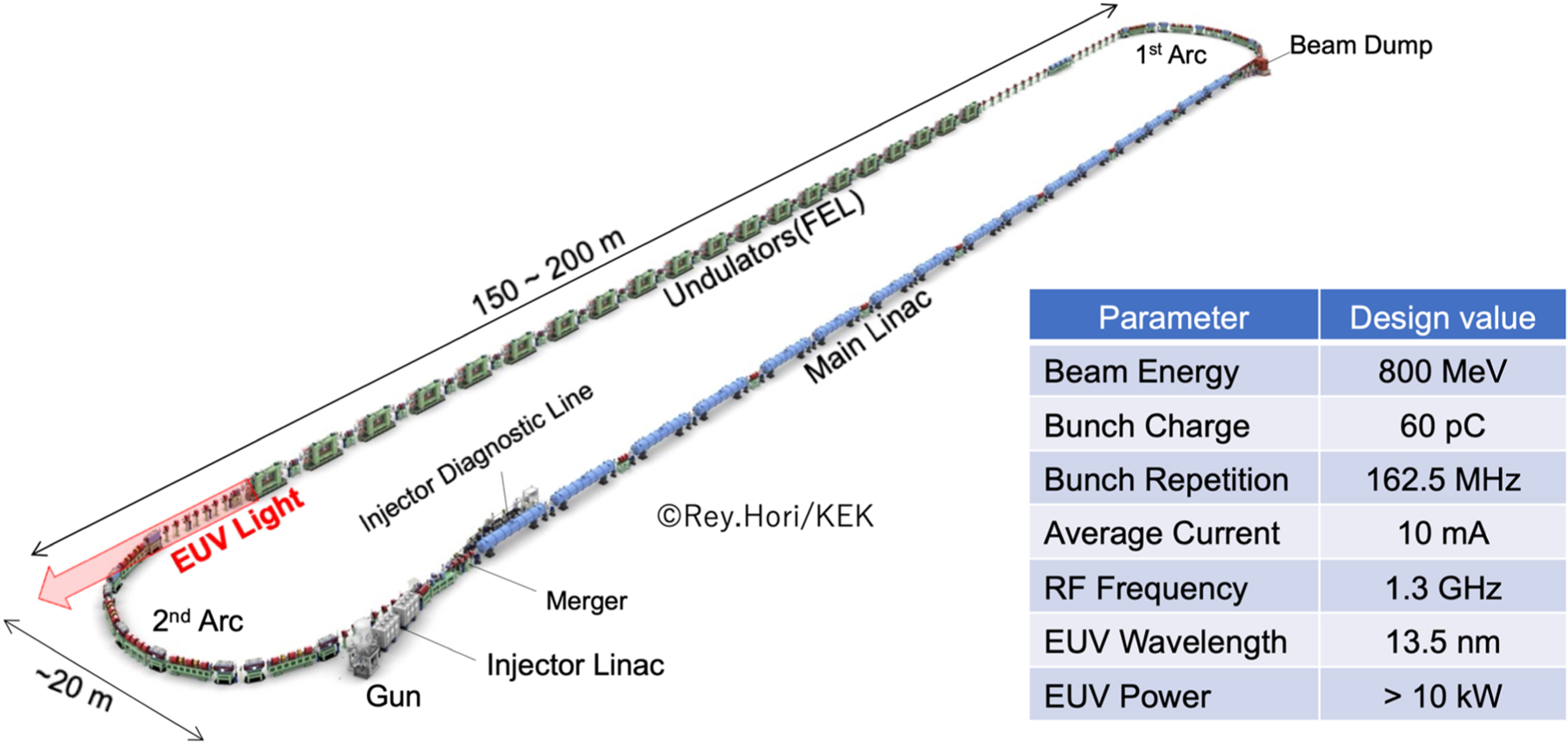
We have designed and studied a high-power EUV-FEL light source based on ERL. 8,9) The illustration and design parameters of the EUV-FEL light source are shown in Fig. 2. In this light source, the electron beam with the bunch charge of 60 pC generated by the electron gun at the bunch repetition frequency of 162.5 MHz is first accelerated to about 11 MeV in the injector SC linac and then to 800 MeV in the main SC linac. The accelerated beam is longitudinally compressed by magnetic bunching in the 1st arc section in order to generate the high-power EUV light by the FEL system with many undulators in the recirculation loop. After the FEL lasing, the electron beam is returned to the main SC linac in the decelerating RF phase via the 2nd arc section, decelerated for energy recovery in the main linac and then dumped at the beam dump. By this energy recovery scheme, the high average current of 10 mA is achieved to provide the high EUV power of more than 10 kW. The main linac has sixty-four 9-cell SC cavities and the acceleration gradient of 12.5 MV m−1 or higher. The RF frequency of the injector and main linac is 1.3 GHz and the octuple of the bunch repetition frequency.

Fig. 2. Illustration and design parameters of the EUV-FEL light source based on ERL. The electron beam with the bunch charge of 60 pC and the bunch repetition of 162.5 MHz is accelerated up to 800 MeV and recirculated to generate the high-power EUV light (>10 kW) by the FEL system. After the FEL lasing, the electron beam is returned back to the main SC linac for energy recovery and dumped at the beam dump.
Download figure:
Standard image High-resolution imageThe main components of the EUV-FEL light source are a photocathode DC electron gun, 10,11) an injector SC cavity, 12,13) a main-linac SC cavity, 14,15) an undulator 16) for the FEL system and two arc sections for bunch control and suppression of coherent synchrotron radiation effects. 17) Most of these components have been studied and developed at the High Energy Accelerator Research Organization (KEK) and are based on available technologies without too much development to industrialize the EUV-FEL light source as soon as possible. The details of R&D on the main components are described in the references.
The EUV-FEL light source has several advantages in comparison to the LPP source. The EUV-FEL light source can generate high EUV power of more than 10 kW without tin debris and, as a result, it can provide more than 1 kW EUV power for 10 scanners at the same time without tin contamination to Mo/Si mirrors. Furthermore, the EUV-FEL is upgradable to a BEUV-FEL for finer pattering with a shorter wavelength (6.6–6.7 nm). Also, it can variably control the polarization of the FEL light for high-NA lithography. In addition, the electricity consumption and cost per scanner can be reduced. The advantageous features of the EUV-FEL light source are described in more detail below.
2.2. High-power performance
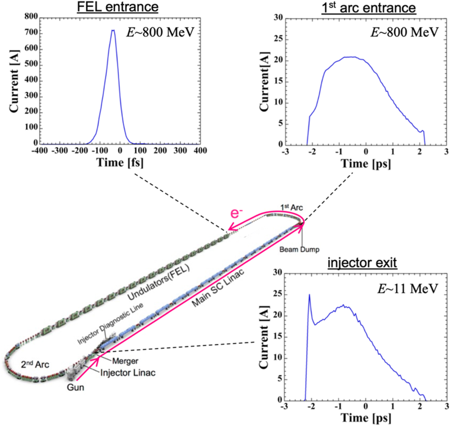
Figures 3 and 4 show the results of a new start-to-end simulation of the EUV-FEL light source to demonstrate its high-power performance. In this simulation, a new optimization of the injector parameters 18) is used to minimize the longitudinal emittance in place of the transverse emittance at the injector exit. Longitudinal space charge (SC) effects are newly introduced in the whole light source for more accurate and realistic simulation. The tracking particle number of 500 k is used in this simulation. Figure 3 shows simulated electron-bunch profiles with the bunch charge of 60 pC at the injector exit, at the 1st arc entrance after the main-linac acceleration to 800 MeV, and at the FEL entrance after magnetic bunch compression in the 1st arc section. The light-source parameters are optimized to maximize the FEL parameter 5) (Pierce parameter) at the FEL entrance. The peak current of the electron bunch at the FEL entrance is greatly increased to higher than 700 A by the bunch compression. The bunch length and energy spread are 39 fs and 0.1% in rms, and the normalized horizontal and vertical emittances are 2.0 and 0.9 mm·mrad.

Fig. 3. Bunch profiles of the electron beam for the bunch charge of 60 pC at the injector exit, at the 1st arc entrance, and at the FEL entrance optimized by simulation from the gun to the FEL entrance with the tracking particle number of 500 000. The peak current at the FEL entrance is greatly increased to more than 700 A by the magnetic bunching in the 1st arc section for the FEL.
Download figure:
Standard image High-resolution image
Fig. 4. (a) Simulated FEL pulse energy per electron bunch of the EUV-FEL light source as a function of the undulator section length with untapering and an optimum linear tapering of 4% and (b) FEL power spectrum at the FEL exit. The calculated EUV-FEL power with 4% tapering is 17.8 kW at 9.75 mA for the bunch repetition frequency of 162.5 MHz and 35.5 kW at 19.5 mA for 325 MHz. The bandwidth of the EUV-FEL spectrum is sufficiently narrow for that of the Mo/Si mirror reflectivity shown by a broken line.
Download figure:
Standard image High-resolution imageFigures 4(a) and 4(b) show the simulated FEL pulse energy per electron bunch as a function of the undulator section length and FEL power spectrum at the FEL exit. Since microbunching of the electron beam with a period of the FEL wavelength grows in the undulators and the microbunched beam radiates the EUV light coherently, the FEL pulse energy drastically increases until it is saturated at 50 ∼ 60 m as shown in Fig. 4(a). The FEL pulse energy with the optimum linear tapering of 4% is 109.4 μJ at the FEL exit and, as a result, the FEL power is 17.8 kW for the bunch repetition frequency of 162.5 MHz at about 10 mA. If the bunch repetition frequency can be doubled to 325 MHz, the EUV power is increased to 35.5 kW at about 20 mA. The simulation result demonstrates that the EUV-FEL light source has excellent high-power performance. The FEL spectral width is less than 0.1 nm and narrow enough for that of Mo/Si mirror reflectivity as shown in Fig. 4(b). The energy spread is significantly increased from 0.1 to 0.34% due to the FEL emission. However, in this simulation, the electron beam is successfully transported without any beam loss even after the FEL lasing through the beam ducts with typical apertures. Three simulation codes, GPT, GENESIS and ELEGANT, are used for the simulations in the injector, the FEL system and the other parts including the main linac and recirculation loop, respectively. Further simulation study is needed for the unconsidered effects of beam dynamics and various errors.
2.3. Optical beamline
An optical beamline is needed to transport the EUV light from the EUV-FEL light source to scanners in the LSI Fab. The energy density per pulse of the EUV-FEL light of the normal incidence is about 10 mJ cm−2 with a transverse size of ∼1 mm2 and the FWHM pulse length of ∼100 fs at 3 m from the FEL exit. It is lower than the ablation thresholds of Mo/Si multilayer and Si, which are experimentally estimated to be about 20 mJ cm−2 by using two light sources, a plasma-based laser and an EUV-FEL at SACLA-BL1, and does not depend on the pulse length for less than 10 ps. 19) Furthermore, in the conceptual design of the optical beamline, the FEL light is first vertically expanded by a curved grazing mirror and then horizontally expanded and separated for ten scanners by a segmented multi-curved mirror, as shown in Fig. 5. 9) The energy density of the EUV light is reduced to about 2.5 μJ cm−2 at 3 m from the segmented multi-curved mirror. After expansion and separation of the FEL light, a collimator mirror system can well adjust the light size for each scanner system. These mirrors are total reflection mirrors with very small glancing angles and can totally reflect the EUV light without ablation damage. Therefore, the EUV light from the light source is transported to the first Mo/Si reflection mirror of each scanner system without significant loss and mirror damage.

Fig. 5. Handling of the EUV-FEL light in the optical beamline. (a) Vertical expansion of the EUV-FEL light by a curved grazing mirror with a small glancing angle. (b) Horizontal expansion and separation of the EUV-FEL light by a segmented multi-curved mirror. The FEL energy density is reduced to 2.5 μJ cm−2 from 10 mJ cm−2 by these total reflection mirrors in the optical beamline. Adapted from Ref. 9.
Download figure:
Standard image High-resolution image2.4. Upgrade scheme to a BEUV-FEL
Figures 6(a) to 6(c) schematically show three possible upgrade schemes to BEUV-FELs from the EUV-FEL light source. The first scheme in Fig. 6(a) is very simple and based on a single-loop layout. Since the FEL wavelength is inversely proportional to the square of the beam energy for the same undulator period and field, the main-linac length is increased by about a factor of the square root of 2 and the beam energy is increased up to 1.13–1.14 GeV to shorten the wavelength to 6.6–6.7 nm, about a half of the EUV wavelength. The undulator section length is also increased because the FEL saturation length is proportional to the beam energy. The other two schemes are based on a double-loop layout not to increase the light source length significantly. In the first double-loop layout shown in Fig. 6(b), the main linac is increased in total length but separated into two parts. The combiner and spreader, each of which may consist mainly of three or four bending magnets, should be designed and added to connect the two loops without significant degradation of the beam quality. The two beams with different energies were merged by the combiner and split by the spreader. In the double-loop layout shown in Fig. 6(c), the beam is accelerated twice by the main linac and, as a result, the main linac length is unchanged or can be decreased. Instead, the beam current and heat load in the main linac become almost double. We can choose one of them suitable for the site size and light-source conditions such as allowable cavity heat load. Most of the EUV-FEL components can be reused in the BEUV-FEL light source in every scheme. Figure 6(d) shows the simulated BEUV-FEL spectrum. 20) The bandwidth of this spectrum (∼0.04 nm) is narrower than that of the measured BEUV mirror reflectivity in Fig. 6(e). 21) This means that an ERL-based FEL is also a promising light source for BEUV lithography.

Fig. 6. Three possible upgrade schemes to a BEUV-FEL based on (a) single-loop layout, (b) double loop layout with the main linac divided into two parts and (c) double loop layout by twice acceleration using half of the main-linac or shorter. (d) Simulated BEUV-FEL spectrum. Adapted with permission from Ref. 20. (e) Measured BEUV mirror reflectivity. Adapted with permission from Ref. 21.
Download figure:
Standard image High-resolution image2.5. Polarization control
The polarization of the FEL light can be utilized for high-NA lithography. The lithography resolution is inversely proportional to NA as shown in Eq. (1) and higher resolution is achieved by higher NA even if the light-source wavelength is unchanged. Figures 7(a) and 7(b) show a schematic of two plane waves propagating on different paths in high-NA configuration and the light intensity produced by the interference of the two waves as a function of the position on a wafer for the s-polarized and p-polarized modes. The light intensities in the s-polarized and p-polarized modes are respectively given by

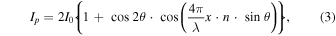
where θ is the incident angle, n is the refractive index, x is the horizontal position on the focal plane and I0 is the intensity of each incident plane wave. NA is defined by n·sinθ and n equals unity in air. In the s-polarized light, the electric fields of the two waves fully interfere at x = 0 because they are parallel. On the other hand, in p-polarized light, the electric fields only partially interfere because they have different directions. The image contrast defined by (Imax−Imin)/(Imax + Imin) is 1 for the s-polarized light and cos2θ for the p-polarized light. The intensity and contrast of the p-polarized light decrease with the incident angle. As a result, the s-polarized light has better performance in high-NA lithography compared to the p-polarized light. Such polarization effects in high-NA configuration were also experimentally demonstrated. 22) Therefore, polarization control of the FEL light is important to make the most of the polarization effect in high-NA lithography.

Fig. 7. Schematic of two plane waves propagating on different paths in high-NA configuration and the light intensity given by the interference of the two waves as a function of the horizontal position, x, on a wafer for the (a) s-polarized and (b) p-polarized modes.
Download figure:
Standard image High-resolution imageWe propose the polarization control scheme for the EUV-FEL and BEUV-FEL light sources shown in Fig. 8. In the FEL system, circularly-polarizing (helical) undulators are used for most of the undulators to have a higher FEL gain and power compared to linearly-polarizing undulators. On the other hand, variably polarizing undulators equipped with a polarization control mechanism are used for the last several undulators. Variably-polarizing undulators such as Apple-2 type 23) can control the polarization of the undulator light by sliding four magnet arrays and generate horizontal and vertical linear polarizations as well as circular polarization. Microbunching of the electron beam grows well in the helical undulators, while the FEL light from the helical undulators is lost and diluted in the undulator section. The final polarization state of the FEL light from the microbunched beam is primarily decided by the variably-polarizing undulators in the downstream. As a result, the EUV-FEL and BEUV-FEL light sources can well control the polarization of the FEL light for high-NA lithography.

Fig. 8. Polarization control scheme of the EUV-FEL and BEUV-FEL light sources. In the FEL system, most of the undulators are circularly polarizing (helical) undulators to have higher FEL gain and power, and the last several undulators are variably polarizing undulators to well control the polarization of the FEL light for high-NA lithography.
Download figure:
Standard image High-resolution image2.6. Electricity consumption and cost
In the semiconductor society, the sustainable semiconductor technologies & systems (SSTS) program was recently introduced, 24,25) because the CO2 footprint of semiconductor manufacturing is rapidly rising. In the technology development of chips, the environmental score is newly added to the traditional ones such as power, area, performance, and cost of chips. From this point of view, the reduction of the electricity consumption of the EUV source is important in EUV lithography because the LPP source has a large portion of the consumed electric power of the EUV lithography exposure tool. Table I shows the estimated electricity consumption of the EUV-FEL light source. The refrigerator system for the SC cavities uses the most electric power of all the items. The infrastructure includes a cooling-water system, an air-conditioning system, an illumination system, and so on. The total electricity consumption is 7 MW for 10 kW EUV power, and hence 0.7 MW per 1 kW EUV power or scanner. On the other hand, the LPP source consumes ∼1.1 MW electric power for 250 W EUV power 26) and ∼4.4 MW for 1 kW EUV power. Although it should be noted that ASML has gradually reduced the electric power required for their LPP sources, 27) the EUV-FEL can greatly reduce the electricity consumption per scanner or 1 kW EUV power and fit the SSTS program.
Table I. Electricity consumption of the EUV-FEL light source.
| Item | Electric power [MW] |
|---|---|
| Refrigerator System | 3.2 |
| RF Source | 1.3 |
| Other Components | 1.0 |
| Infrastructure | 1.5 |
| Total | 7.0 |
The cost of the EUV source is also important in the technology development of chips. The construction and running costs of the EUV-FEL light source are roughly estimated to be US$400 M and US$40 M year–1 for 10 kW EUV power and hence US$40 M and US$4 M year−1 per 1 kW EUV or scanner. On the other hand, the construction and running costs of the LPP light source are roughly estimated as US$20 M and US$15 M year−1 per 250 W EUV power and US$80 M and US$60 M per 1 kW EUV power or scanner by simple linear extrapolation. Especially the running cost of the LPP source is expensive and the maintenance expense of the collector mirror, which is degraded due to the contamination of tin debris and frequently replaced with a new one, takes up the majority of the running cost, though the lifetime of the collector mirror has been significantly improved. 1) The EUV-FEL light source can also reduce the construction and running costs per scanner. A similar comparison of the costs between LPP and EUV-FEL sources was previously performed. 28)
3. PoC of the EUV-FEL using cERL
Demonstration of the PoC of the EUV-FEL is also important. The cERL 29) was constructed at KEK in 2014 and has been operated to develop key ERL technologies such as a photocathode DC gun and an SC cavity and to show the potential of the excellent ERL performance as future light sources and industrial applications. Operation at the average current of about 1 mA with low bunch charges (<6 pC) was already achieved with energy recovery in the cERL. 30,31) PoC of the EUV-FEL can be provided by installing FEL undulators in the cERL for generation of SASE-FEL emission, as shown in Fig. 9. The wavelength of undulator light, λ, is given as follows:


where γ is Lorentz factor, aw is the rms undulator parameter, Brms is the on-axis rms magnetic field, λu is the magnetic period of the undulator, me and e are the of electron mass and charge, and c is the speed of light. As shown in Eq. (4), the wavelength is inversely proportional to the square of the electron beam energy, Ee = γme c2. Typically, the magnetic period is a few centimeters and the rms undulator parameter is around unity. Therefore the cERL generates IR light by FEL undulators in place of EUV light because of the low electron-beam energy. So far only oscillator FELs have been operated in the ERLs and an SASE-FEL has never been operated in ERL layout. Higher peak current and beam quality of the electron beam are generally required for an SASE-FEL than for an oscillator FEL. An IR-FEL at the cERL will be the first ERL-based SASE-FEL in the world if achieved and can be the PoC of the EUV-FEL light source based on ERL. The bunch charge is set at the high bunch charge of 60 pC, which is needed for lasing the FEL and the same bunch charge as that of the EUV-FEL light source.

Fig. 9. 3D Illustration and present parameters of the cERL including an SASE-FEL, which can serve as PoC of the EUV-FEL light source.
Download figure:
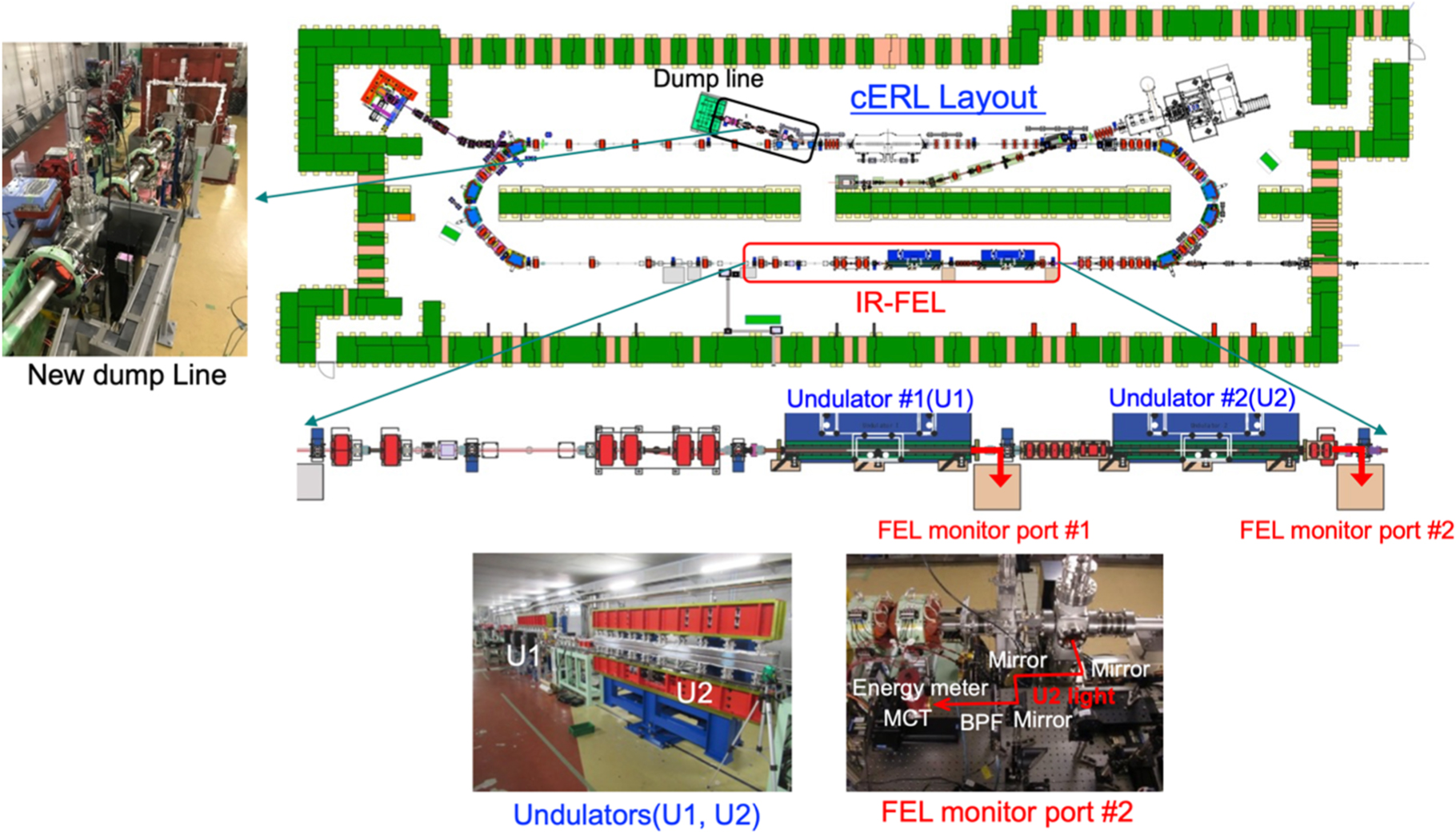
Standard image High-resolution imageFortunately, an IR-FEL was constructed in the cERL from October 2019 to May 2020 as a NEDO project for the purpose of developing high-power mid-infrared lasers for highly-efficient laser processing utilizing photo-absorption based on molecular vibrational transitions. 32) This can also serve as the PoC of the EUV-FEL light source based on ERL. The cERL layout including the IR-FEL is shown in Fig. 10. Two 3 m undulators U1 and U2 were installed with two FEL monitor ports for the IR-FEL. Since the project budget was limited, linearly-polarizing adjustable phase undulators (APUs) with a magnetic period of 24 mm were adopted as the FEL undulators for cost reduction. These undulators can change the magnetic field by sliding the upper magnetic array longitudinally for a fixed magnetic gap of 10 mm to change the wavelength. For cost savings of the EUV-FEL light source, variably- and circularly-polarizing APUs with a fixed gap should be developed in future. Each FEL monitor port has two kinds of monitors for the IR-FEL light, an MCT (HgCdTe) detector and an energy meter (a pyroelectric sensor). The electron beam energy is about 17.5 MeV and the undulators cover the FEL wavelength of 10 to 20 μm. In addition, since the energy acceptance normalized by the beam energy of the dump line was the smallest in the cERL, the cERL dump line was reconstructed in Autumn 2020 to improve the energy acceptance greatly for avoiding serious beam loss in future high-power FEL operation. 33)

Fig. 10. Layout of the cERL surrounded by the concrete radiation shield. In the reconstruction area for the IR FEL (in a red frame), two 3 m undulators, U1 and U2, were installed with two FEL monitor ports. The dump line (in a black frame) was also reconstructed to improve the energy acceptance for reducing the beam loss for future high-power FEL operation. Photographs of the two undulators, the FEL monitor port of U2, and the new dump line are also shown.
Download figure:
Standard image High-resolution imageFigure 11 shows the FEL operation scheme. In the FEL commissioning and beam tuning, we used Burst mode, where a macro-pulse of about 1 μs is repeated at 5 Hz as shown in Fig. 11(a). In the future, we will perform high-power FEL operation in CW mode, where the electron bunch is continuously repeated as shown in Fig. 11(b). The bunch-length control scheme for the IR-FEL operation is shown in Fig. 11(c). The electron bunch from the injector is accelerated off-crest in the main linac and then the energy-chirped bunch is compressed in the 1st arc by magnetic bunching to increase the peak current for the FEL. After the FEL emission, the bunch is dumped to the movable dump via the 2nd arc in Burst mode. In CW mode, the bunch is decelerated in the main linac for energy recovery and then dumped to the main beam dump via the dump line. The transverse beam size and position are well-tuned in the undulator chambers with a very narrow vertical aperture by using the focusing and orbit-correction magnets in the upstream and the beam profile monitors in the undulator section.

Fig. 11. Time structure of the cERL electron beam (a) in Burst mode and (b) in CW mode. (c) Bunch-length control scheme. In the scheme, the electron bunch is accelerated by the injector and the main linac is compressed in the 1st arc by magnetic bunching to increase the peak current for the FEL. After the FEL emission, the electron bunch is dumped to the movable dump in Burst mode and the main dump in CW mode.
Download figure:
Standard image High-resolution imageFigure 12 shows the FEL commissioning results from February to March 2021. 32) In this commissioning, machine learning was introduced to enhance the speed and skills of beam tuning. You can see in Fig. 12(a) that the FEL intensities of U1 and U2 monitored by the MCT detectors were well maximized by machine learning. Time variation of the FEL energies of U1 and U2 measured by the MCT detectors and output signals from the energy meters for U1 and U2 are shown in Figs. 12(b) and 12(c). Figure 12(d) shows the FEL pulse energies per electron bunch of U1 and U2 at the FEL wavelength of 20 μm as a function of the undulator section length. The blue and red lines in this figure are the simulated FEL pulse energy from U1 and U2 for the target electron-beam parameters and the two red circles are the FEL pulse energies of U1 and U2 measured by the energy meters. The measured FEL energy of U2 was significantly lower than the simulated one because the beam parameters were not good as compared to the target ones. The main cause of the relatively low FEL pulse energy of U2 is the SC effects, which strongly affect low-energy beams, and our simulation study suggests that significant SC effects cannot be avoided in the cERL. The SC force becomes stronger where the electron density is higher and, as a result, lengthens the electron bunch that is magnetically compressed in the 1st arc to increase the peak current and hence reduces the FEL pulse energy. They also induce increasing the energy spread and transverse emittances of the beam. Therefore beam control and tuning in a low-energy machine such as the cERL are more difficult due to the SC effects than in a high-energy one like the EUV-FEL light source. However, you can see in Fig. 12(d) that the FEL pulse energy of the NEDO-project goal was almost achieved taking into account the air absorption in the optical path to the detector. Such significant SASE-FEL emission at the cERL IR-FEL is a very important step of the PoC of the EUV-FEL. Toward future high-power FEL operation in CW mode, the first beam transport study in the new dump line was conducted in Autumn 2021. 33) Moreover the first high-current operation after the IR-FEL construction was carried out with a low bunch charge and no FEL emission in February to March 2022 and the maximum current of about 250 μA was achieved with ∼100% energy recovery. 34,35)

Fig. 12. Results of the IR-FEL commissioning. (a) Example of machine learning for maximizing the FEL outputs of U1 and U2. Adapted with permission from Ref. 32. (b) Time variance of the FEL energies of U1 and U2 from the MCT detectors. Adapted with permission from Ref. 32. (c) Output signals from the energy meters for U1 and U2. (d) The FEL pulse energies per electron bunch of U1 and U2 as a function of the undulator section length at the FEL wavelength of 20 μm. The blue and red lines are simulated values of U1 and U2 for the target beam parameters and the two red circles are measured values of U1 and U2 by the energy meters. The green broken line is the NEDO project goal.
Download figure:
Standard image High-resolution image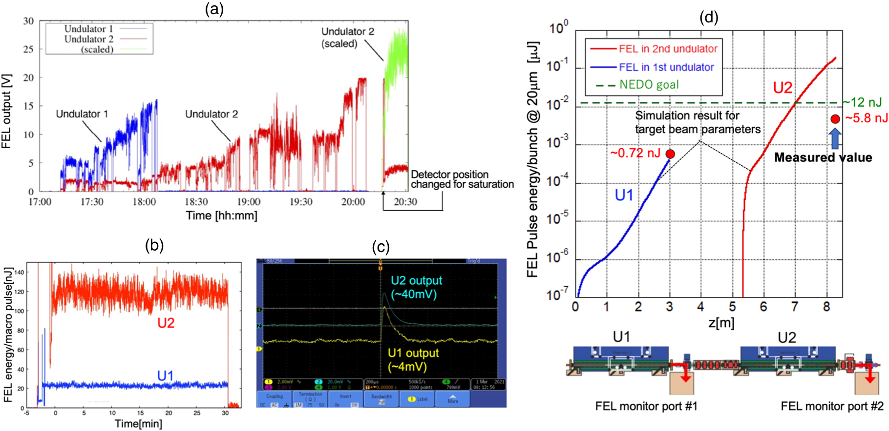
4. Summary
HVM by EUV lithography has recently started based on the 250 W LPP source. However, EUV lithography will need a more powerful EUV source in the future in order to overcome the stochastic effects for higher throughput and higher NA. Therefore, it is still important to develop a higher-power EUV light source. An ERL-based FEL can have extremely high FEL power by the energy recovery scheme and be a promising candidate for a high-power light source for lithography. An EUV-FEL light source based on ERL has been designed for future lithography and the main components have been studied and developed. The EUV-FEL light source offers many advantageous features in EUV power, upgrade to a BEUV-FEL, polarization control for high-NA lithography, electricity consumption and cost per scanner. Excellent high-power performance of the EUV-FEL light source was newly demonstrated by a start-to-end simulation with new optimization and more accurate calculation, and possible schemes or designs of upgrade to a BEUV-FEL, polarization control of the FEL light and an optical beamline from the light source to scanners were studied and proposed. The electricity consumption, construction, and running costs per scanner were estimated for the EUV-FEL and the LPP source and, as a result, it was found that they can be saved by switching to the EUV-FEL light source from the LPP source. Moreover, the generation of significant SASE-FEL emission at the cERL IR-FEL was achieved as an important step in the PoC of the EUV-FEL. Further progress has been made toward the future high-power FEL operation. The EUV-FEL light source is concluded to be a most promising light source for future lithography and should be more promoted for industrialization.
Acknowledgments
The authors would like to thank the EUV-FEL Light Source Study Group for Industrialization and all the members of the cERL collaboration team and the NEDO project team. This work is partially supported by a NEDO project "Development of advanced laser processing with intelligence based on high-brightness and high-efficiency laser technologies."