
Abstract
In this paper, development of NuFlare Technology's multi-beam (MB) mask writing system MBM-2000 series is reviewed, and future plans for the MBM series are discussed. The MB mask writing systems were designed on the basis of unique concepts suitable for high-volume production of leading-edge masks, i.e. high beam current density, a reliable beam blanking aperture array (BAA) system with a 50 keV single-stage acceleration optics, high-speed inline pixel-level dose correction, and a distinctive hardware system for charging effect reduction. The latest MB mask writing system, MBM-2000PLUS, achieves a high throughput of 8.7 h in a 104 × 130 mm2 writing area for a 150 μC cm−2 resist thanks to a high beam current density of 3.2 A cm−2. In addition, a global position accuracy of 1.2 nm, a local position accuracy of 0.5 nm, and a local critical dimension uniformity of 0.61 nm are achieved. The BAA system has shown long-term stable operation for more than one year. The high productivity and writing accuracy realized by NuFlare Technology's concepts will contribute to further miniaturization of semiconductors.
Export citation and abstract BibTeX RIS
1. Introduction
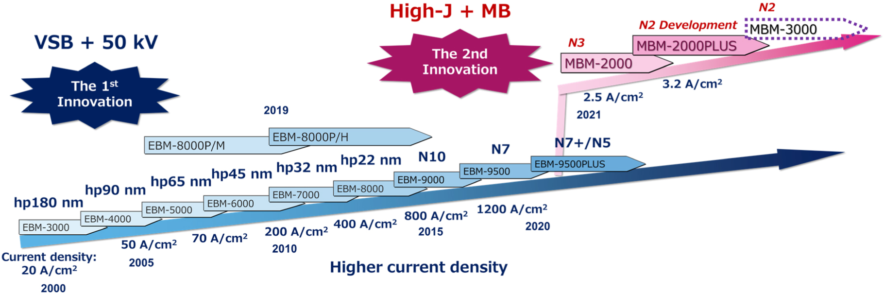
Electron-beam (EB) lithography systems are used in a variety of applications. For example, direct writing systems are used for research and development of futuristic devices 1) and mask writing systems are used for advanced mask production. 2) Productivity and writing accuracy of the EB writing systems are very important factors, especially in mask production. In recent leading-edge mask manufacturing, two different methods are utilized: the single variable-shaped beam (SVSB) writing and the multi-beam (MB) writing. SVSB writing has been mainly used for the semiconductor design nodes down to 5 nm (N5), and MB writing is used for beyond it. 2) NuFlare Technology has been developing both SVSB 3–9) and MB mask writing systems 10–20) (Fig. 1). New models have been introduced every few years to meet the demand cycle of semiconductor miniaturization and higher precision. As part of this trend, beam current density has been increased and writing accuracy has been improved.

Fig. 1. (Color online) Overview of the history of NuFlare Technology's EB mask writers.
Download figure:
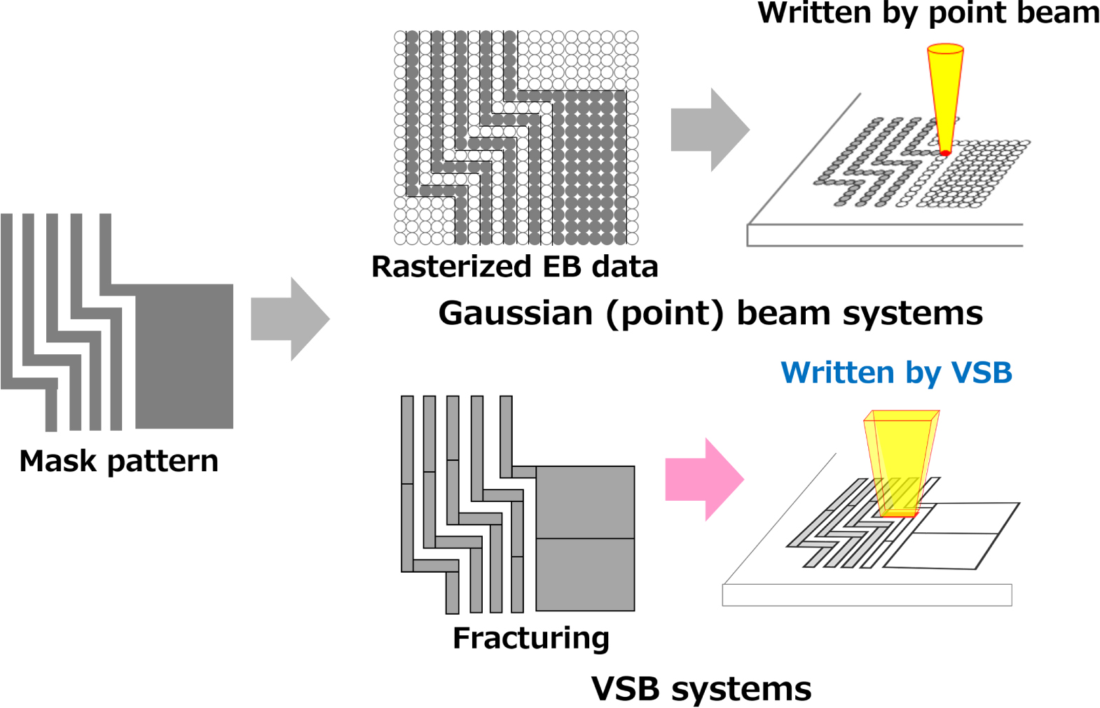
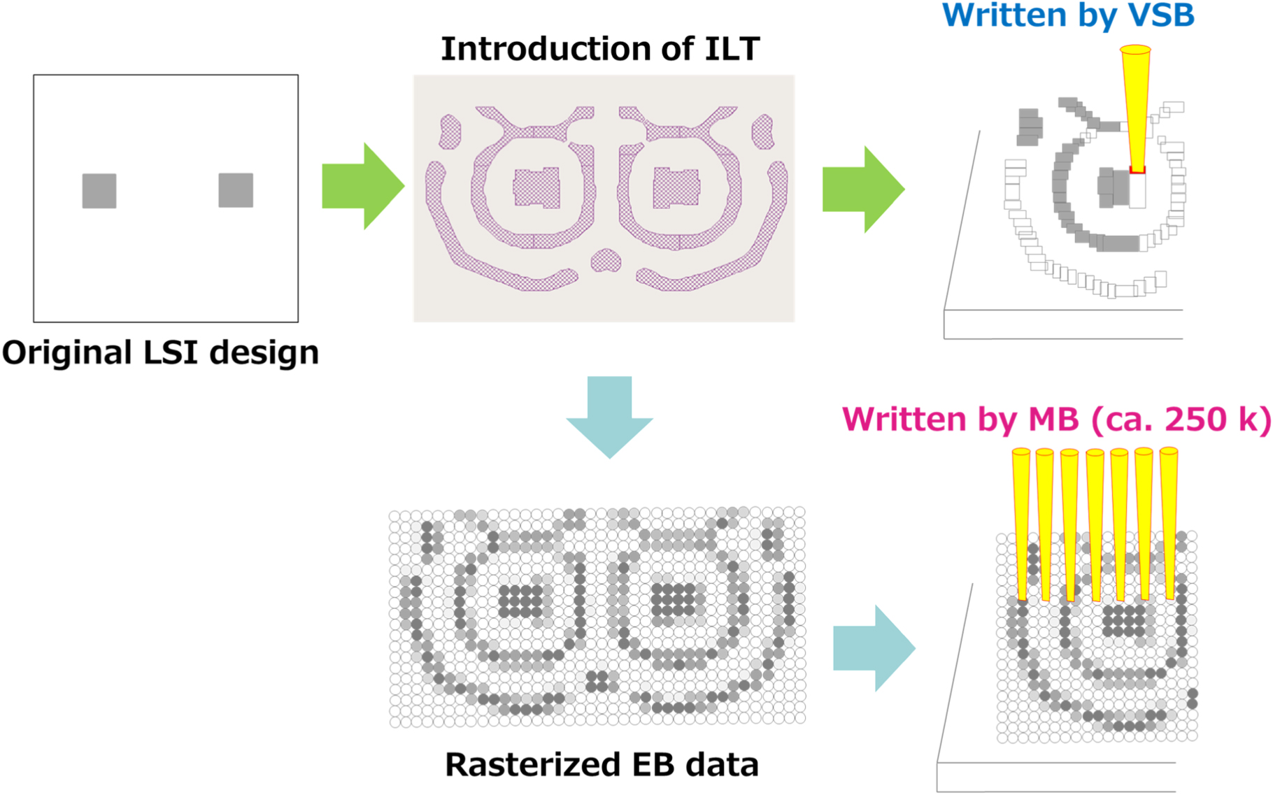
Standard image High-resolution imageThere have been two key innovations in the development of the mask writing systems. The first occurred in the late 1990s to early 2000s. During that time, SVSB systems were developed by Toshiba Machine (the predecessor of NuFlare Technology), Hitachi, 21–23) and JEOL, but Gaussian (or point) beam systems from ETEC 24) were mainly used. In the latter systems, inputted mask pattern data is converted to pixel data, and the mask pattern is written by a point beam in raster scanning (Fig. 2). Although a finer pattern can be written by reducing the beam spot size, the shot count increases drastically, resulting in an increase in write time. In contrast, in SVSB systems, the design data is fractured into variable-shaped shots; accordingly, the shot count is significantly reduced. Eventually, the SVSB systems came to dominate mask manufacturing. 3–9,21–23) The SVSB technology, however, faces difficulties beyond the 5 nm node, where the introduction of inverse lithography technology 25–27) makes LSI design no longer simple like a complex curve pattern (Fig. 3). To write this kind of complex curve pattern with the SVSB systems, it has to be divided into many tiny shots, resulting in an increase in write time again. To address this issue, MB mask writing systems have been develope. 10–20,28–31)

Fig. 2. (Color online) Schematic of writing strategy image of Gaussian beam systems and variable-shaped beam tools.
Download figure:
Standard image High-resolution image
Fig. 3. (Color online) Schematic of writing strategy image of SVSB systems and multi-beam systems in advanced lithography.
Download figure:
Standard image High-resolution imageIn the MB mask writing system, mask data is rasterized to pixel data in the same manner as the conventional Gaussian beam one. However, the key difference from the Gaussian beam system is the use of a massive number of MB ca. 250 k beams to reduce the write time to be practical. Another key feature is that the write time is constant no matter how small and complex the pattern is since the pixel area is constant. Due to these features, the MB mask writing systems play a key role in mask production beyond the 5 nm node.
NuFlare Technology released the MBM-2000 18) in 2021, which was designed to accomplish high throughput in the 3 nm node (N3) by increasing the beam current density to 2.5 A cm−2. In 2022, the MBM-2000PLUS 19,20) was released for developing the 2 nm node (N2). The beam current density was increased to 3.2 A cm−2, enabling the use of a lower sensitivity resist down to 170 μC cm−2. In this paper, the concepts and the key features of NuFlare Technology's MB mask writing systems are described in Sects. 2 and 3, respectively. After showing results of writing performance, some improvement items for the future MBM series are discussed in Sect. 4.
2. Concepts of MBM series
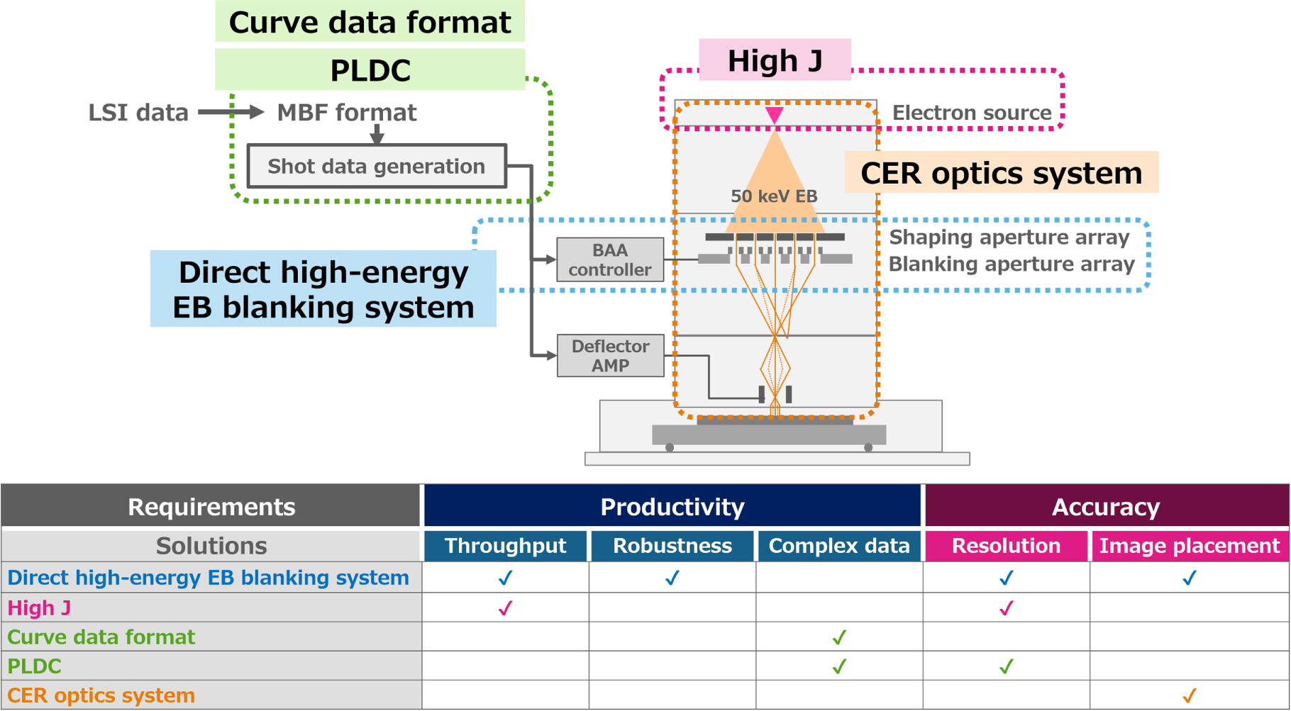
The requirements for MB mask writing systems are categorized into productivity and writing accuracy, as shown in Fig. 4. For the productivity, high throughput is one of the most important requirements for mask manufacturing, and a reasonable write time is necessary even for low-sensitivity resist to accomplish better pattern fidelity. 32–35) Robustness is also required to minimize system downtime and improve productivity. In addition, smarter data handling is required for complex curve data to reduce computing power and the cost of ownership. 36–38) In terms of writing accuracy, strict demands are placed on image placement accuracy as well as resolution, line-edge roughness, and critical dimension (CD) uniformity. 2,39,40) To meet these requirements, NuFlare Technology's MB mask writing systems have beneficial features (Fig. 4).

Fig. 4. (Color online) Requirements for MB mask writing system and NuFlare Technology's solutions.
Download figure:
Standard image High-resolution imageThere are several types of key elements to realize electron MB for a single column system, e.g. a blanking aperture array (BAA) and a digital pattern generator (DPG). The DPG was developed for the reflective electron-beam lithography by KLA-Tencor. 41,42) The BAA is used in the MB mask writing systems developed by NuFlare Technology and IMS Nanofabrication. Basically, both MB mask writing systems have almost the same configuration in terms of MB formation and control, except for the accelerating optics, i.e. the number of acceleration stages. NuFlare Technology adopts a 50 keV single-stage acceleration optics, while IMS Nanofabrication does a double-stage acceleration optics where a 5 keV MB is accelerated to 50 keV after passing a BAA. 28–31) Nuflare Technology's direct blanking operation of such a high-energy beam accomplishes higher accuracy thanks to it being less sensitive to external noise in all beam paths. Furthermore, it enables simple and robust electrical insulation design because it does not need an additional high potential area that may cause unexpected discharges. The BAA system is described in more detail in Sect. 3 as the first key feature.
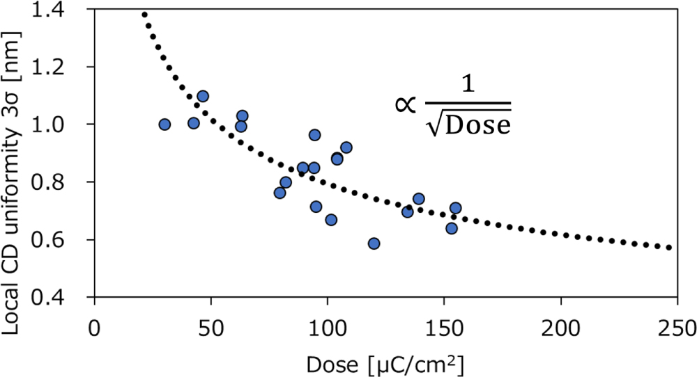
The second key feature is high beam current density (J). In mask fabrication of the 5 nm node and beyond, the demand for lower sensitivity resists is growing sharply because it is widely understood that the shot noise, which is a statistical fluctuation of an electron's distribution in resist, is a dominant factor to degrade CD uniformity and line-edge roughness.
32–35) Figure 5 shows the relationship between dose and local CD uniformity (LCDU). The LCDU is improved proportionally to  which is a general relationship between noise intensity and averaging number. Therefore, the exposure dose for leading-edge mask production is becoming higher to meet the strict demands for CD uniformity, line-edge roughness, and pattern fidelity. To achieve a reasonable write time (T) even in those high dose conditions, NuFlare Technology has designed a new brighter electron source that enables higher beam current density to be emitted. One of the major challenges in achieving such a high beam current density is to extend the lifetime of the electron source. The new brighter electron source has achieved a long lifetime of one year.
19,20) The write time of MB mask writing systems is mainly determined by data transfer time (tdata) to transfer shot data to BAA, or beam exposure time. The beam exposure time is proportional to the exposure dose and inversely proportional to J. Accordingly, the write time is as described below,
which is a general relationship between noise intensity and averaging number. Therefore, the exposure dose for leading-edge mask production is becoming higher to meet the strict demands for CD uniformity, line-edge roughness, and pattern fidelity. To achieve a reasonable write time (T) even in those high dose conditions, NuFlare Technology has designed a new brighter electron source that enables higher beam current density to be emitted. One of the major challenges in achieving such a high beam current density is to extend the lifetime of the electron source. The new brighter electron source has achieved a long lifetime of one year.
19,20) The write time of MB mask writing systems is mainly determined by data transfer time (tdata) to transfer shot data to BAA, or beam exposure time. The beam exposure time is proportional to the exposure dose and inversely proportional to J. Accordingly, the write time is as described below,

where W is total writing area, m is number of beamlet, and bs is beam size.

Fig. 5. (Color online) Relationship between LCDU and dose.
Download figure:
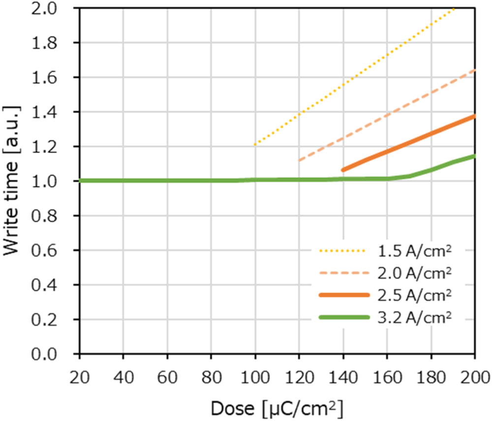
Standard image High-resolution imageFigure 6 shows the relationship between the write time and the exposure dose. In a low dose area, the write time is constant because the data transfer time is the constraining factor; beam exposure is finished within the data transfer time. In high dose area over 100 μC cm−2, however, beam exposure time exceeds the data transfer time and total write time increases as the exposure dose becomes higher in the lower J case as shown by dotted and dashed lines in Fig. 6. On the other hand, in the MBM-2000PLUS, the write time is constant continuously up to 170 μC cm−2 thanks to its higher beam current density of 3.2 A cm−2.

Fig. 6. (Color online) Relationship between write time and dose for MB mask writing system.
Download figure:
Standard image High-resolution imageThe other features, curve data format, pixel-level dose correction (PLDC), and charging effect reduction system are described in the following section.
3. Key features of MBM series
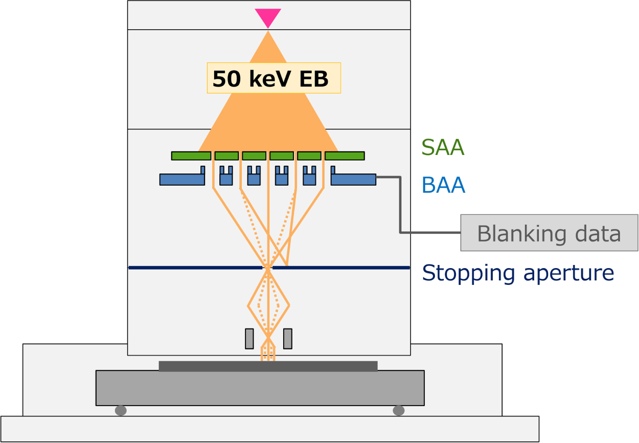
3.1. Blanking aperture array
Figure 7 shows a system configuration diagram of the MB mask writing system including electron optics. The EB emitted from the electron source is accelerated to 50 keV and split into ca. 250 k square beamlets by a shaping aperture array (SAA). A BAA is placed just below the SAA. A voltage is applied to deflection electrodes of the BAA by a driver circuit in accordance with blanking data. Each beamlet is independently deflected by the electric field generated between the electrode pair. The beamlets slightly deflected by the BAA (dotted lines) are cut off by a stopping aperture below. Finally, the entire beamlet that has not been deflected by BAA (solid lines) is positioned on a mask blank. Beam blanking and positioning operations are controlled in synchronization with the stage motion to form a latent image pattern with desired doses in the resist.

Fig. 7. (Color online) System configuration diagram of MB mask writing system.
Download figure:
Standard image High-resolution imageFigure 8 shows a cross sectional diagram of the BAA with an equivalent driver circuit. The BAA is fabricated by using conventional LSI and microelectromechanical system (MEMS) technologies. Blanking electrodes and through-holes are formed on and inside a LSI chip by the MEMS process. A driver circuit is connected to each blanking electrode applying a voltage to control blanking operation individually. As mentioned above, NuFlare Technology's MB mask writing system adopts a single-stage acceleration system that deflects the 50 keV EB as is. This concept requires some special designs and configurations of the BAA system against radiation damage due to the high-energy EB, but it gives us a very important advantage. The high-energy beam is less sensitive to external noise such as charging, so it is suitable for obtaining high writing accuracy. Stable operation for about one year has been confirmed at our users' sites.
Fig. 8. (Color online) Cross sectional diagram of BAA with equivalent driver circuits.
Download figure:
Standard image High-resolution image3.2. Data-path and correction function
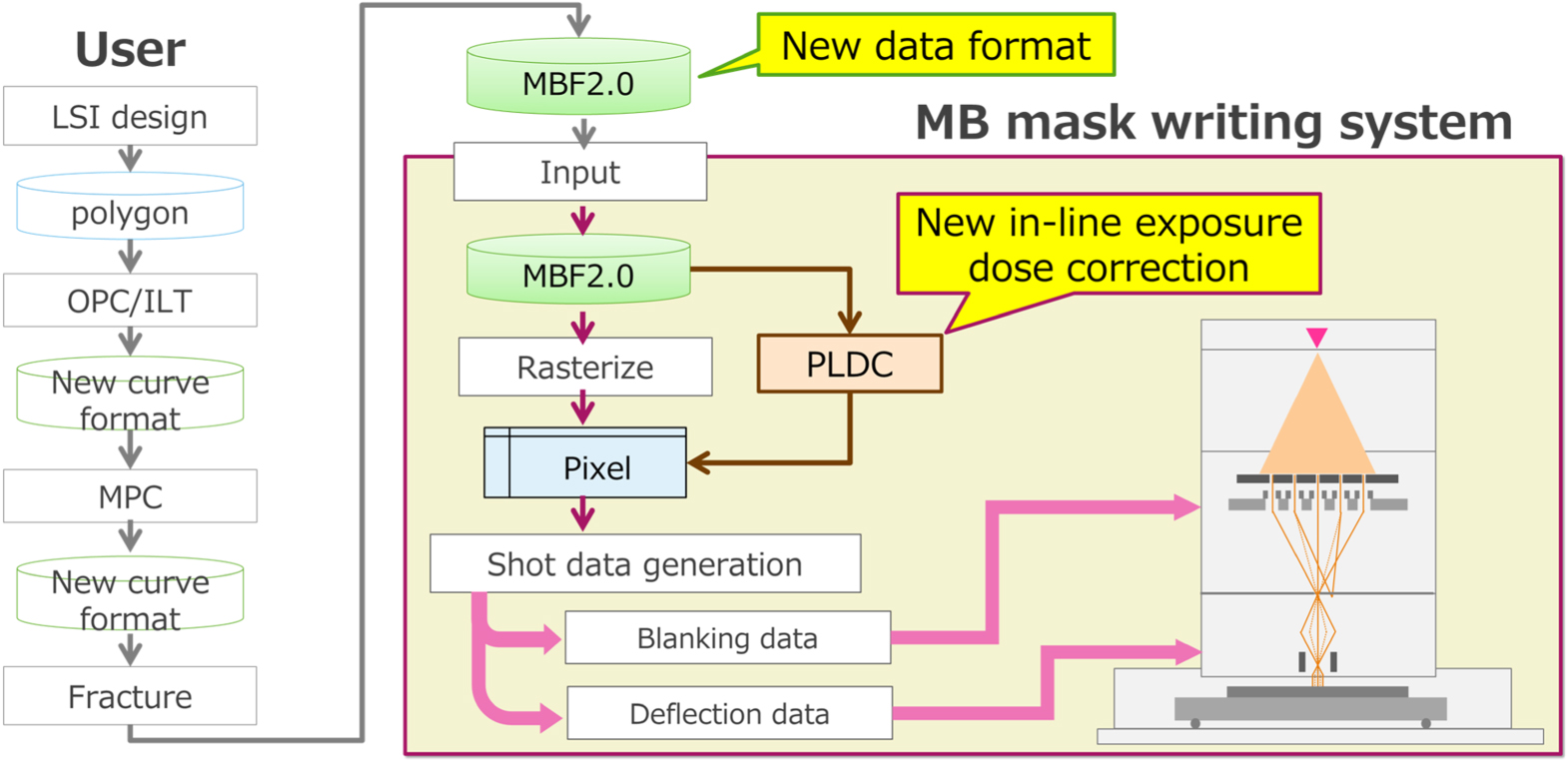
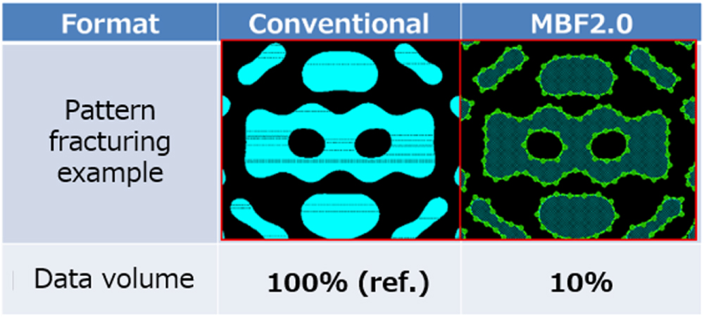
Another feature is data-path for pixel-by-pixel data generation instead of figure-by-figure data, which is conventionally used in the SVSB systems. Figure 9 shows the overall illustration of the data-path flow. In the conventional representation using rectangular figures, the number of figures becomes huge, especially for the curve patterns that are the target of MB mask writing, and the amount of data becomes impractically large. Consequently, a new data compression format is needed. NuFlare Technology has developed the new data format MBF2.0 for efficient layout expression. In the MBF2.0, figures are expressed by control points of the B-spline curve and the data volume is compressed to 10% compared with conventional rectangle expression in the curvilinear pattern case as shown in Fig. 10.

Fig. 9. (Color online) Overall illustration of data flow in MB mask writing system.
Download figure:
Standard image High-resolution image
Fig. 10. (Color online) Data expression comparison of conventional data format and MBF2.0.
Download figure:
Standard image High-resolution imageThanks to its dose control by a fine pixel area smaller than the target pattern size, our MB mask writing systems can carry out PLDC within a reasonable write time. 18–20,43) In SVSB, the same fine area control results in impractically long write time due to massive shot counts. The PLDC has various functions such as enhancing the lithographic process margin, correcting CD linearity, and improving pattern fidelity. Those corrections are accomplished with no additional turn-around time (TAT) because the corrections are processed in the background of writing. Here, we explain the PLDC focusing on the improvement of pattern fidelity by edge enhancement. Figure 11 shows dose profiles with and without edge enhancement. The dose gradient at the edge is increased by edge enhancement. Thus, it reduces edge placement errors and improves fidelity.
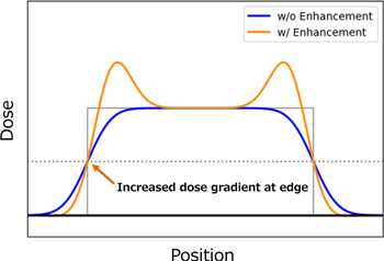
Fig. 11. (Color online) Dose profiles with and without edge enhancement.
Download figure:
Standard image High-resolution imageTo verify fidelity improvement quantitatively, we used the transfer function method. 19,20) In this method, sine-shape patterns are used [Fig. 12(a)]. The pattern edge shape can be expressed by one convolutional operation with a Gaussian function with a size of σedge as below,

where A is amplitude and λ is period of the designed sine-shape. The σedge represents total blur including gray error σgray, beam blur σbeam, and process blur σprocess, as written below


Fig. 12. (Color online) (a) Scanning electron microscope (SEM) image of sine-shape. (b) Comparison of ideal sine-shape (dashed line) and contour results of written pattern extracted from SEM images (colored lines).
Download figure:
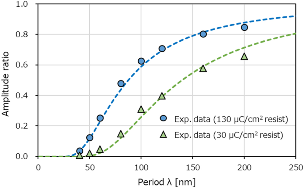
Standard image High-resolution imageEquation (2) means that the ratio of amplitude of actual patterned sine-shape to that of the ideal sine-shape decreases depending on λ as shown in Fig. 12(b). Furthermore, the less σedge the steps from an ideal pattern to actual pattern have, the less the amplitude ratio is reduced in sine-shape with small λ and high frequency. Figure 13 shows experimental results written with the MBM-2000 for verifying Eq. (2) by using two different processes at NuFlare Technology's site: one is the previous generation with 30 μC cm−2 resist, and the other is the current generation with 130 μC cm−2 resist. The current generation process has a smaller value of σprocess than the previous generation process. The improvement of σedge by σprocess changing in the current generation process can be clearly observed as the amplitude ratio increases from the previous process in the small λ region. Therefore, the sine-shape pattern is a useful metrology pattern to evaluate the indicator, σedge.

Fig. 13. (Color online) Experimental results of amplitude ratio of actual patterned sine-shape to that of design one with different λ and two different process. The design amplitude of sine-shape is 40 nm.
Download figure:
Standard image High-resolution imageThe improvement of pattern fidelity by the PLDC was verified with the transfer function method. Figure 14 shows the experimental results with and without the PLDC function on blanks with the 130 μC cm−2 resist and NuFlare Technology's current generation process. It can be seen that σedge with the PLDC is smaller than that without PLDC because the amplitude ratios of the PLDC in the small λ region are larger. The experimental results are fitted by theoretical function  of Eq. (2) and different σedge, σPLDC ON, and σPLDC OFF are obtained for results with and without PLDC. By considering σPLDC ON is effective pattern fidelity with PLDC writing, the enhancement ratio of σedge by PLDC function is obtained by

In other words, a 16% enhancement of pattern fidelity by PLDC was verified.

Fig. 14. (Color online) Comparison of the experimental results with and without PLDC function. The dashed lines are theoretical function  of Eq. (1) and different σedge, σPLDC ON and σPLDC OFF.
Download figure:
Standard image High-resolution image3.3. Charging effect reduction system
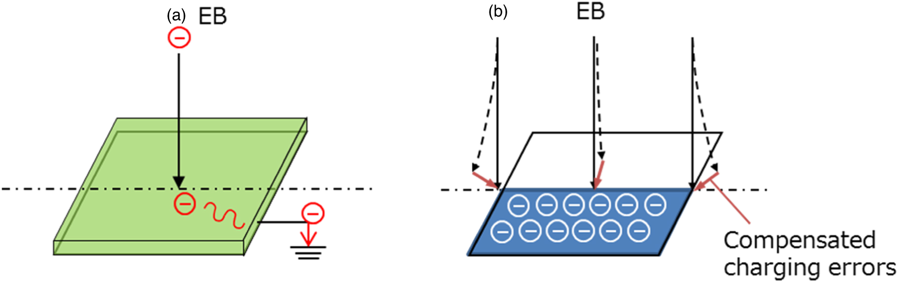
The resist surface charging effect is one of the critical error sources in image placement (IP) accuracy. There are two major solutions to address the charging effect: using mask blanks with a charge dissipation layer (CDL) that has conductivity to relieve the surface charge 44) [Fig. 15(a)], and using a charging effect correction (CEC) system 45–50) [Fig. 15(b)]. One of the main factors of the charging effect is low-energy secondary electrons (LSEs) that return to the resist surface after being generated by irradiation of the primary EB. The resist surface charging effect is generally the same for SVSB and MB mask writing systems. 50) However, the main difference is the total exposure dose. This is because the sensitivity of a typical resist used in MB is about three times higher than that of SVSB. As discussed in Sect. 2, lower sensitivity resists are required for leading-edge mask fabrication. Therefore, the contribution of the LSEs increases due to an increase in the number of primary electrons, resulting in a larger charging effect. In advanced lithography, these two major solutions face several challenges. For the CDL, the conductivity of CDL needs to be high enough to quickly relieve the surface charge of LSEs. Otherwise, the charge accumulation will cause non-negligible placement errors. As for the CEC, it needs to predict the complicated charge distribution including that of LSEs, which is affected by the electromagnetic field of an optical system and pre-existing resist surface charge. The amount of resist surface charge varies nonlinearly with the exposure dose, which is modulated at the mask writing on the basis of local pattern density as a consequence of proximity effect correction. Those charge variations make the CEC model complex. In both cases, the amount of LSEs needs to be reduced to achieve higher placement accuracy. Therefore, NuFlare Technology has developed a charging effect reduction (CER) system, 50) which is a hardware solution to reduce LSEs contributing to resist surface charge by a mechanical and electromagnetic design of electron optics.

Fig. 15. (Color online) Conceptual illustration of (a) CDL and (b) CEC.
Download figure:
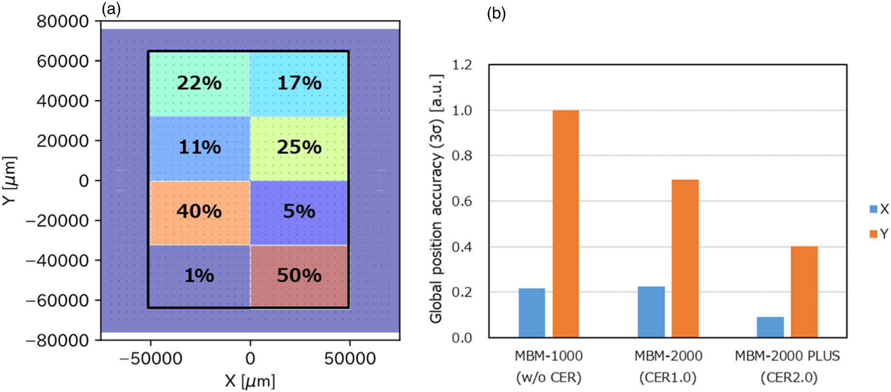
Standard image High-resolution imageTo verify the effectiveness of the CER design, we evaluated the amplitude of global position (GPOS) error from resist surface charge in the test layout as shown in Fig. 16(a). The layout has the main chip consisting of eight pads with pattern densities from 1% to 50% and position marks covering the main chip area. The sets of CEC parameter were obtained for the MBM series in different configurations: non-CER, CER1.0 and CER2.0. We calculated the amplitudes of the GPOS error from resist charge without CEC by using the CEC model and the CEC parameter sets [Fig. 16(b)]. The GPOS error was seen to reduce, and that in CER2.0 is reduced by approximately 60% compared with non-CER. These results indicate that the CER design successfully reduces LSEs and improves IP accuracy.

Fig. 16. (Color online) (a) The layout for evaluation of GPOS error from resist charge and CEC. (b) The amplitudes of GPOS errors from resist charge expected for the test layout, with MBM series in non-CER, CER1.0 and CER2.0 configurations.
Download figure:
Standard image High-resolution image4. Results and discussion
4.1. System specification and writing performance
Table I shows the configuration and specifications of the MBM-2000 and the MBM-2000PLUS. For the MBM-2000PLUS, the beam current density and the data processing time are increased to reduce the write time for use of low-sensitivity resist and to handle more complex data, respectively. Its new optics with the CER2.0 design are upgraded to reduce the beam position error from resist charge so that the system achieves a GPOS accuracy of 1.3 nm. The LCDU is improved to 0.65 nm by using lower sensitivity resists and beam performance improved with the new optics.
Table I. Configuration and specifications of MBM series.
| Item | MBM-2000 | MBM-2000PLUS |
|---|---|---|
| Acceleration voltage | 50 kV | 50 kV |
| Beam current density | 2.5 A cm−2 | 3.2 A cm−2 |
| Total beam current | 1.7 μA | 2.1 μA |
| Beam size | 16 nm | 16 nm |
| Stripe height | 82 μm | 82 μm |
| Number of beamlets | 250 k | 250 k |
| Data format | MBF (polygon/curve support) | ← |
| Correction function a) | PEC/FEC/LEC, GMC, CEC, PLDC | ← |
| Optics design | CER1.0 | CER2.0 |
| Writing time | 8.7 h (130 μC cm−2 resist) | 8.6 h (130 μC cm−2 resist) |
| (104 × 130 mm2 area) | 9.5 h (150 μC cm−2 resist) | 8.7 h (150 μC cm−2 resist) |
| Writing accuracy | ||
| Global position (3σ) | 1.4 nm | 1.3 nm |
| Local position (3σ) | 0.7 nm | 0.7 nm |
| Local CD uniformity (3σ) | 0.7 nm (130 μC cm−2 resist) | 0.65 nm (150 μC cm−2 resist) |
a)PEC: proximity effect correction, FEC: fogging effect correction, LEC: loading effect correction, GMC: grid matching correction, CEC: charging effect correction, PLDC: pixel-level dose correction.
Writing results are summarized in Fig. 17. The GPOS accuracy was evaluated with the same test layout shown in Fig. 16(a). In Fig. 17(a), the writing result indicates that the GPOS accuracy with the CEC and the glass thermal expansion correction (GTEC) is 1.2 nm, which meets the MBM-2000PLUS specification of 1.3 nm. Figure 17(b) shows the local position accuracy and the result is 0.5 nm, meeting the specification of 0.7 nm. No signature of stripe boundary is recognized in the local position error map. Figure 17(c) shows the distributions of LCD errors in the vertical and horizontal directions. The obtained LCDUs are both 0.61 nm, which meets the specification of 0.65 nm.

Fig. 17. (Color online) (a) GPOS accuracy, (b) LPOS accuracy, and (c) LCDU performance of MBM-2000PLUS.
Download figure:
Standard image High-resolution image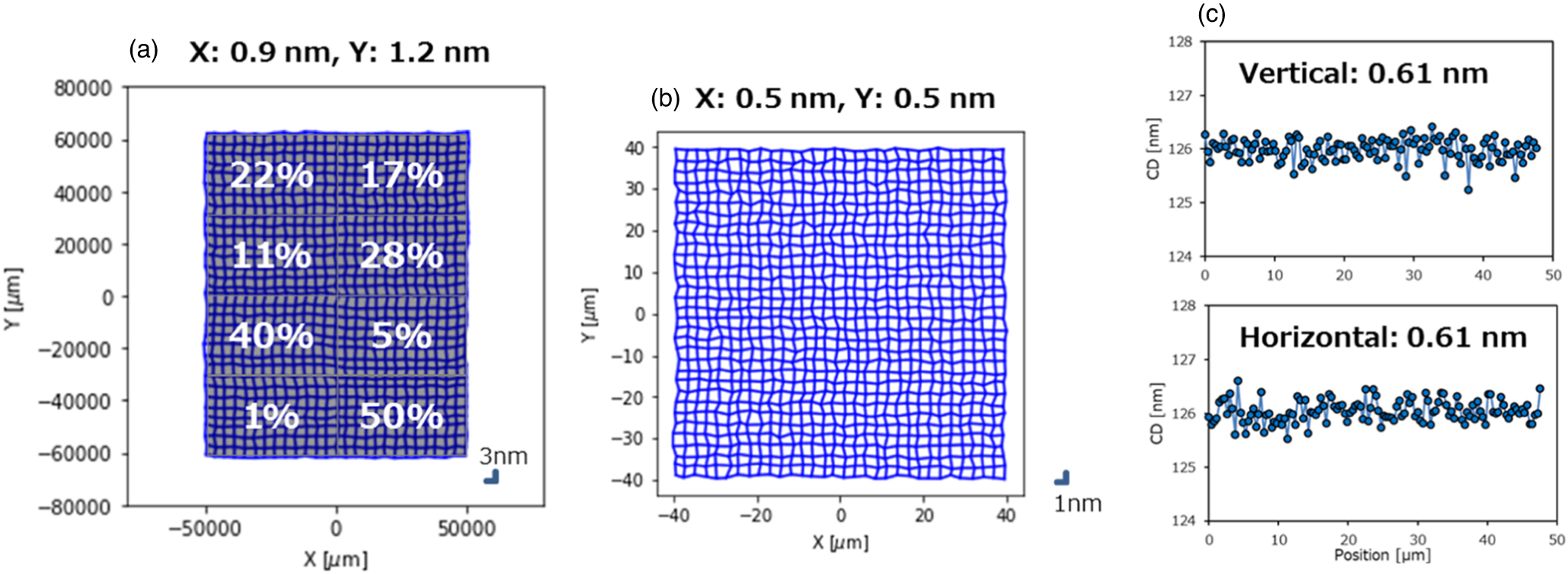
4.2. Future of MBM series
Further miniaturization of semiconductors is expected in the foreseeable feature thanks to the development of high-NA extreme ultraviolet (EUV) lithography, 51) and thus the requirements for mask writing systems will keep becoming stricter. To meet these requirements, high resolution should first be achieved. The resolution is composed of different components as expressed by the exposure intensity distribution (EID) as below

where Ms is rasterizing mesh size, Bs is beam size, Bb is beam blur, and Pb is process blur. Equation (5) indicates that reducing Bs is a key point to improve resolution. In hardware, this is related to a SAA. In terms of beam blur (Bb ), beam array distortion and the Coulomb interaction effects need to be reduced. In general, increasing beam current density will degrade beam resolution due to the Coulomb interaction effects. 30,52–56) This will be addressed by optimizing the electron optical parameters that affect the effects. Optimizing writing strategy including the PLDC, which is related with Ms and Bb , is also a key element.
IP also requires higher accuracy. 2,39,40) To improve the IP accuracy, the charging effects are key points. For the charging effects at glass plate and its resist surface, we will upgrade the CEC and CER. As for the charging effects at an objective deflector, a beam drift correction system will be upgraded. In addition to the high accuracy in general IP, tool stability and tool matching are also key elements because stitching will be needed when using a high-NA EUV lithography system. 51) In such cases, a single-stage acceleration optics with a robust BAA will be more attractive.
Sufficient throughput will be needed to meet requirements for high-volume manufacturing. As mentioned above, to achieve high resolution, beam size will be reduced, and thus the write time will increase because it is inversely proportional to beam size as described in Eq. (1). To cover this, the beam current density and the beamlet number will be increased by upgrading the electron source and BAA system, respectively. The electron source will be designed to achieve a long lifetime. The BAA data rate will also be increased to reduce the data transfer time. To obtain better productivity, suppress the computing power, and reduce the cost of ownership, curvilinear data handling will be improved by an upgraded MBF data format. As for increasing productivity, stage maintainability also will be improved. In short, many elements need to be developed to meet the stricter requirement for the next-generation mask writing systems. However, all key elements are being developed by NuFlare Technology, and thus optimization between elements will be a competitive advantage.
5. Summary and conclusions
High-performance multi-beam (MB) mask writing systems were successfully developed on the basis of NuFlare Technology's unique concepts. The BAA, one of the most important features for the MB mask writing systems, showed long-term stable operation for more than one year with a 50 keV single-stage acceleration optics. Another key feature is the data-path for the pixel-by-pixel data generation. The pixel-level dose correction (PLDC) function has achieved super-resolution with no additional turn-around time (TAT). The resist charging effects are the most critical error sources in the image placement (IP) accuracy. We have addressed these issues with software (charging effect correction (CEC)) and hardware (charging effect reduction (CER)) solutions and have achieved high IP accuracy. Thanks to these key features, the MBM-2000 series is used for extreme ultraviolet (EUV) mask writing at our users' sites. Our future plans include reducing beam size and increasing beam current density to improve resolution and throughput simultaneously, contributing to further miniaturization of semiconductors.