
Abstract
A new optimization method for femtosecond-laser-written lithium niobate (LN) waveguides is proposed and experimentally demonstrated to achieve low propagation loss. In this method, we use Raman spectroscopy to find detailed structural changes in LN crystal. We then use the results to optimize the laser irradiation conditions, including pulse laser energy, and laser irradiation design. In order to confirm the validity of this method, depressed cladding type LN waveguides were formed and their structural and optical characteristics were investigated in detail. Using proposed method, we succeeded in fabricating depressed cladding type LN waveguides with low propagation loss (∼0.64 dB cm−1) in the communications wavelength band. Furthermore, by analyzing the crystal structure of the depressed cladding waveguide cross-section using a Raman spectroscopy mapping system, the asymmetry of the waveguide cladding was newly clarified, providing a new insight for further improvement of the optical properties.
Export citation and abstract BibTeX RIS
1. Introduction
The nonlinear optical crystal, lithium niobate (LN), is a promising candidate for optical switches, modulators, frequency combs, and phase sensitive amplifiers due to its large electro-optic response, high second-order nonlinearity, and wide transparency window. 1–5) For nonlinear integrated photonic systems in particular, LN waveguides are attracting great attention because they have higher optical density than bulk LN crystals through light confinement in the waveguide core, which results in higher performance. 6–8) LN waveguides have been fabricated mostly by using the proton exchange method, titanium (Ti) diffusion method, or dry etching technique. 9–11) However, these fabrication methods have the following problems: high fabrication cost due to the need for a clean room process, relatively slow fabrication throughput, and low flexibility in waveguide design (i.e. only two-dimensional structure can be fabricated).
As a method to solve the above problems, femtosecond laser writing has been attracting much research interest. Femtosecond laser writing in transparent materials such as polymer, glass, and crystalline materials has been used to produce optical waveguides. 12–16) In this technique, an optical waveguide is formed by using structural changes induced by laser irradiation. The advantages compared with previous methods are low manufacturing cost, no need for a clean room process, and high flexibility in waveguide design, including three-dimensional structures. For depressed cladding in particular, the laser-written area can be used as a cladding because the laser-irradiated area has a low refractive index compared with the unirradiated area. 17–20) As such, femtosecond laser writing can be used to fabricate waveguides with various core shapes by drawing the cladding into the materials even in three dimensions. However, femtosecond-laser-written waveguides have been fabricated and their optical properties evaluated without understanding the effect of femtosecond laser irradiation on their structural properties. At the same time, there have been a few reports on the crystal structural changes induced by laser irradiation to LN, 21–23) but the understanding of how the crystal structure changes in an actual laser-written LN waveguide is still insufficient. Thus, it has been difficult to find the laser-writing conditions and waveguide design in efficient way to produce waveguides with good optical properties, including low propagation loss.
In this paper, we propose a new method for femtosecond laser writing to prepare low-loss LN waveguides using Raman spectroscopy. 24,25) The advantage of Raman spectroscopy is that it allows quantitative evaluation of structural changes even under conditions where cracks do not occur but the crystal structure is damaged. The effect of femtosecond laser irradiation on the structural properties of LN crystals is investigated in detail by using Raman spectroscopy. From the results, we clarify the correlation between the laser irradiation conditions and structural changes. Applying these new insights to the femtosecond-laser-writing process, we succeeded in fabricating a depressed-cladding LN waveguide with low propagation loss (∼0.64 dB cm−1). This is the first example of the use of Raman spectroscopy to determine the conditions for the formation of a waveguide with small propagation loss. In addition, Raman mapping measurement of the LN waveguide cross-section provides new insights into the crystal structure changes actually occurring in the fabricated waveguide.
2. Experimental methods
Femtosecond laser processing was performed on zinc (Zn)-doped LN. Figure 1 shows a schematic of the optical system for femtosecond laser irradiation. A LN chip with dimensions of 15(x) × 8(y) × 0.3(z) mm3 was used. The laser was swept parallel to the crystal x-axis. The pulse irradiation interval with respect to the propagation direction was 0.95 μm. The end face of the chip was optically polished before femtosecond laser processing.
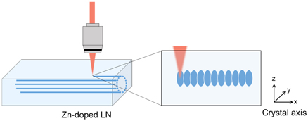
Fig. 1. (Color online) Schematic image of optical system for femtosecond laser writing system.
Download figure:
Standard image High-resolution imageFor femtosecond laser processing, we used a femtosecond laser with a wavelength of 1030 nm, pulse width of 600 fs, and pulse energy of around 360 nJ. The pulse energy was optimized based on the results of Raman spectroscopy (shown later). The femtosecond laser beam was focused onto the sample using an objective lens with 20 × magnification (NA = 0.4), and the irradiation position was controlled by using a motorized three-axis stage. The programmed positions were precisely irradiated by the pulses, which was controlled by the output acousto-optic modulator of the laser, and the trigger signal to the modulator was generated synchronously with the position of the xyz stage. Microscopic images of the cross section were acquired by using a polarized light microscope in transmission mode.
Raman spectroscopy was performed with a commercially available confocal Raman microscopy system (LabRAM HR Evolution, HORIBA Jobin Yvon). The excitation light wavelength was set to 532 nm. The spatial resolution was about 1 μm.
The propagation loss of the LN waveguide in the communication bands was obtained by the Fabry–Perot method using following equation.
where K is the fringe contrast, R is the Fresnel reflectance, α is the propagation loss, and L is the propagation length. Propagation loss α can be expressed by the following equation
This measurements were performed with a wavelength sweep in the wavelength range of 1544.9 to 1545.1 nm. Since fabrication errors such as flatness of the waveguide end face affect the measured value in the Fabry–Perot method, an average value was used for the waveguide propagation loss.
The z-axis polarized incident light was used to characterize the optical properties. The temperature of the chip during the optical measurement was set to 40 °C. Near-field mode profiles of the depressed-cladding LN waveguide were measured by imaging the output surface with a microscope objective and a charge-coupled device (CCD) camera.
3. Results and Discussion
3.1. Investigation of irradiation conditions by Raman spectroscopy
First, to analyze the changes in the crystal structure of LN due to the laser irradiation in detail, Raman spectroscopy with a confocal microscope was performed for the unirradiated and irradiated area. Figure 2(a) shows the design for the laser irradiation to evaluate Raman spectra. The irradiation interval was set to 2 μm, and the number of irradiation points was 16. An optical microscope image of the irradiated area is shown in Fig. 2(b). The black and red dot indicate the position of the measured unirradiated (black) and irradiated (red) areas, respectively. Figure 2(c) shows the Raman spectra of LN crystals in the unirradiated (black) and irradiated (red) area. A sharp peak originating from the Nb–O stretching mode is detected around 613 cm−1. 26–28) The peak intensity decreased and the full width at half maximum (FWHM) increased with laser irradiation. These data indicate that laser irradiation induces amorphization of the LN crystal.
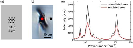
Fig. 2. (Color online) (a) Design for the laser irradiation to evaluate Raman spectra. (b) Optical microscope image of irradiation area. The black and red dots indicate the position of the measured unirradiated (black) and irradiated (red) areas, respectively. (c) Raman spectra of LN crystal in the unirradiated (black) and irradiated (red) area.
Download figure:
Standard image High-resolution imageNext, the pulse energy was optimized by using the FWHM of the Raman peak as an indicator of amorphization. The optimal value of the pulse energy would be one where the crystal structure changes to decrease the refractive index to form a cladding, but cracks do not appear. The pulse energy dependence of structural change is shown in Fig. 3. In this study, 16 points with intervals of 2 μm were irradiated in the LN (shown in inset of Fig. 3). The FWHM of the peak around 613 cm−1 was monitored as an indicator of amorphization and the pulse energy was varied from 252 to 630 nJ. The FWHM of laser unirradiated area is shown as dashed line. Optical microscope images of the cross sections corresponding to each pulse energy are also shown in Fig. 3. With increasing pulse energy, the FWHM gradually increased up to around 315 nJ, then rapidly increased and saturated above 379 nJ. This result indicates that amorphization began with pulse energy of around 315 nJ. As seen in the optical microscope images of the cross sections, the LN crystal began to crack with irradiation above 441 nJ, which is undesirable in the waveguide process. Therefore, the optimum laser irradiation energy was predicted to be 379 nJ.

Fig. 3. (Color online) Irradiation design, optical microscope images, and FWHM at Raman peak around 613 cm−1 as a function of pulse energy.
Download figure:
Standard image High-resolution imageIn what follows, we investigate the intervals between the irradiation points, which is an important parameter for the optimum design of depressed-cladding waveguides. Since the structure of the cladding affects the light confinement in the core and also the scattering of light in the direction of light propagation, it is an important parameter for forming a waveguide with low propagation loss. In particular, a flat refractive index profile with low periodicity of the structural change is preferable for achieving low propagation loss. To realize the low periodicity, the irradiation interval was optimized by using the FWHM of the Raman peak at 613 cm−1 as an indicator of amorphization by changing the irradiation intervals. Figure 4 shows the y-axis line profiles of the FWHM for irradiation intervals of 2 (black), 3 (red), and 4 μm (green). The inset shows the femtosecond laser irradiation design and optical microscope images. For an interval of 2 μm, there was no periodic structural change in the irradiated region. However, the LN started to crack in the left oblique direction, indicating that the irradiation interval of 2 μm was too small to create a crack-free cladding. When the irradiation interval was 3 μm, small periodicity appeared and no cracks occurred. When the interval exceeded 4 μm, clear periodicity appeared, which is not desirable for fabricating a low-loss waveguide, because of the loose confinement of the light. Based on the obtained data, the appropriate interval between irradiation points is considered to be around 3 μm.
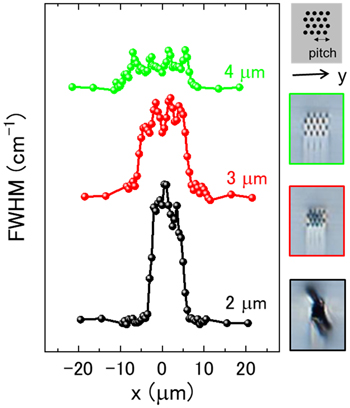
Fig. 4. (Color online) Optical microscope images and line profiles of FWHM at Raman peak around 613 cm−1 as a function of different laser irradiation pitch of 2 (black), 3 (red), and 4 μm (green).
Download figure:
Standard image High-resolution image3.2. Optical characteristics of waveguide produced by proposed method
Based on the fabrication parameters obtained from Raman spectroscopy, we prepared a depressed-cladding LN waveguide and evaluated its optical properties. Figure 5(a) shows the waveguide cross section design. The core diameter, pulse energy, and irradiation interval were set to 30 μm, 379 nJ, 3.1 μm, respectively, which are the values obtained with our proposal method as described above. An optical microscope image of the prepared waveguide is shown in Fig. 5(b). This image shows that the laser was irradiated as designed, and the waveguide structure was accurately formed. The near-field pattern for the single-mode incident light at 1545 nm is shown in Fig. 5(c). Single-mode propagation is observed with the mode-field diameter of about 22 μm. The propagation loss measured by the Fabry–Perot method is 0.64 dB cm−1 at 1545 nm, which is relatively small for depressed depressed-cladding waveguides.

Fig. 5. (Color online) (a) Waveguide design, (b) optical microscope image, and (c) near-field mode profile of depressed cladding type waveguide.
Download figure:
Standard image High-resolution imageTo confirm the validity of the method proposed in this study, we evaluated the optical characteristics of waveguides with different fabrication parameters. Figure 6 shows the averaged loss of two waveguides fabricated with pulse energies of 339 to 392 nJ. The core diameter is 30 μm, and irradiation interval was 3.1 μm. The propagation loss was found to be the lowest for pulse energies between 366 and 379 nJ, a range that includes our predicted value of 370 nJ.
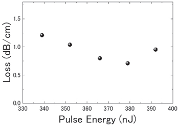
Fig. 6. Relationship between pulse energy and propagation loss.
Download figure:
Standard image High-resolution imageSimilarly, the relationship between the propagation loss and irradiation interval is also investigated. Figure 7 shows the averaged propagation loss of waveguides fabricated with different irradiation intervals. The number of sample waveguides is two for 3.1 um pitch and one for all others. The pulse energy was set to 366 nJ (black) or 379 nJ (red). As expected, the propagation loss was minimized when the irradiation interval was around 3 μm. Below 3 μm, cracking occurred when the pulse energy was 379 nJ. Therefore, the risk of cracking increased when the interval was below 3 μm. It was also found that the propagation loss increased when the irradiation interval was more than 3 μm because of the looser light confinement. In summary, the laser irradiation conditions derived using our proposed method provide low propagation loss without the risk of cracking. Therefore, our method is effective for the optimization of the low-loss-waveguide fabrication process.
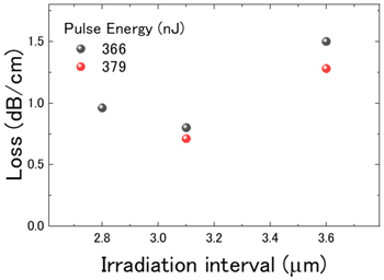
Fig. 7. (Color online) Relationship between irradiation interval and propagation loss at 366 nJ (black) and 379 nJ (red) pulse energy.
Download figure:
Standard image High-resolution image3.3. Characterization of cross-sectional crystal structure for further improvement
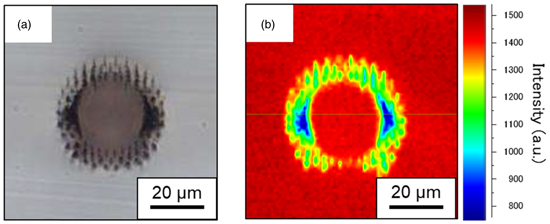
For further improvement of the waveguide characteristics, the crystal structure in the waveguide cross section was analyzed. Raman mapping of the cross section of the LN waveguide structure with a core diameter of 30 μm was obtained to study the crystal structure changes in detail. Figure 8(a) shows an image of the cross section of the LN waveguide taken with a transmission polarization microscope (crystal z-axis polarization). The cross-sectional observation shows that the waveguide is formed to the same design shown in Fig. 5(a). In order to analyze the crystal structure change in the waveguide cross-section, the Raman scattering intensity integrated from 600 to 660 cm−1 was mapped [Fig. 8(b)]. In the optical microscope observation, the cladding appears to be formed in all directions. However, the Raman mapping result reveals that the cladding, i.e. the amorphous area, is actually formed only in the left-to-right direction and not in the top-to-bottom direction. One of the advantage of Raman spectroscopy is that it can quantitatively evaluate structural changes that cannot be determined from optical microscope images. It has long been said that one of the reasons for using a depressed-cladding waveguide is its ability to form an isotropic waveguide structure. However, the Raman mapping result reveals that the structure is not truly isotropic. Therefore, in the future we will attempt to optimize the laser irradiation conditions to fabricate a waveguide structure with a symmetrical shape in order to further improve the optical properties.
Fig. 8. (Color online) (a) Optical microscope image of waveguide cross section where Raman scattering intensity mapping was obtained. (b) Mapping result of Raman scattering intensity integrated from 600 to 660 cm−1.
Download figure:
Standard image High-resolution image
4. Conclusions
In summary, we have proposed a new structure optimization method using Raman spectroscopy for the femtosecond laser writing of waveguides in LN with low propagation loss. By optimizing the laser irradiation conditions based on structural data obtained by Raman spectroscopy, a propagation loss of ∼0.64 dB cm−1 in the communications wavelength band was achieved. The crystal structure of a depressed-cladding waveguide cross-section was analyzed by Raman spectral mapping. As a result, the asymmetry of the waveguide cladding was clarified, which is a new insight for further improvement of optical properties. These results and insights indicate that the structural analysis by Raman spectroscopy is a powerful tool in the femtosecond-laser-writing method, and it is expected to make a significant contribution to the formation of femtosecond-laser-written LN waveguides in the future.
Acknowledgments
We thank Dr. Junji Hirohashi and Dr. Shunsuke Watanabe from Oxide Corporation for their useful advice on waveguide processing.