
Abstract
The stability and robustness of lightly and highly doped poly-Si resistors were evaluated. These resistors exhibited distinct electrical resistance properties and temperature dependences, which can be explained through the grain and grain boundary conduction mechanisms. The resistance shift saturated under the low current stress condition, but continued to increase under the high current stress condition. A novel carrier trapping density model was proposed to explain this behavior. A generalized free energy model that considered stress temperature and stress current dependences was proposed to account for the stability lifetime of a poly-Si resistor based on the resistance shift criterion. Robustness evaluation with transmission line pulse test revealed that the breakdown current exhibited a pulse width dependence which was further explained by a thermal-conduction energy model.
Export citation and abstract BibTeX RIS
1. Introduction
As semiconductor technology nodes continuously scale down, polycrystalline silicon (poly-Si) thin films have been widely used in integrated circuits. 1–3) Poly-Si can be used as a resistor, a gate electrode, an interconnect or an e-fuse according to its doping conditions. Owing to the rapid development of power management modules, passive components inside integrated circuits have become increasingly important. Resistors are key elements that are critical to the design of high voltage circuits, wherein the resistance values considerably affect the circuit performances; thus the precision control of resistance is required. 4) For example, in regulator circuits, the stability and reliability of resistors directly affect the accuracy of voltage supplied to the electrical circuit. 5,6) A poly-Si thin film is the most ideal choice for embedded resistors in CMOS integrated circuit because of its low and stable voltage and temperature coefficients. 7) Many factors influence the electrical properties of the poly-Si resistors during the deposition process, such as process temperature, dopant concentrations, and the overall thermal budget. 8) These conditions also affect the grain sizes and the grain boundaries (GBs), which confer different resistive properties. 9–12) The sheet resistance of a poly-Si thin film is mainly controlled by the dopant concentration, which can be more freely controlled in IC processes. Hence, an in-depth understanding of the effect of doping conditions on resistive properties is critical for the design of reliable resistors.
Previous study has reported that changes in the dopant concentration levels of the poly-Si thin films could give rise to different resistance properties. 13) The electrical properties of lightly and heavily doped poly-Si resistors were reported to differ according to the conduction mechanisms; however, the effects of dopant concentration and stress condition on the resistor's stability or robustness have not been investigated. 14,15) The resistance of poly-Si resistor under stress over time is reported to increase exponentially to the point of saturation. The hydrogen out-diffusion theory based on the GB conduction of poly-Si resistor has been advanced to be the mechanism responsible for the resistivity increase in poly-Si resistors. 16) Although this theory explains that the increment in resistance leads to a final saturation, it does not account for the continuous resistance increment in heavily doped poly-Si resistors, as observed in our study detailed below. 16,17) The tests of electrical current and temperature stress are typically used to assess the stability or reliability of interconnects and resistors in ICs. 18,19) The reliability of silicide and non-silicide poly-Si resistors has been compared and reported. 20) Poly-Si thin film resistors exhibit an Arrhenius temperature dependence of the stability lifetime. 21) The current dependence of poly-Si resistor stability lifetime has been reported to be power law or exponential dependence. To date, time degradation, dopant concentration effect and physical model derivation of poly-Si resistors have not been thoroughly investigated. 22)
In addition to stability as a reliability index, robustness is an important quality index for the application of poly-Si resistors. The transmission line pulse (TLP) test is an important assessment for evaluating the capability of an electrical component to resist short current pulse stress. 23,24) The reliability of poly-Si resistors under pulse voltage stress at different duty cycles and frequencies for a negative temperature coefficient of resistance (TCR) poly-Si resistor was evaluated. However, the analysis of the positive TCR poly-Si resistor or the investigation of the pulse time width dependence of the pulse breakdown pulse current has not been conducted. 25)
In this report, we studied the stability and robustness of poly-Si resistors at different doping concentration levels by analyzing the current and temperature dependences, which is necessary to maintain accurate resistance control. Different resistance properties and time evolution behaviors of poly-Si resistors at different doping concentration levels were investigated. New physical models were developed to explain the evolution of resistance shift, stability lifetime, and pulse width dependence of the TLP failure current. This paper is an extension of our previous study, 26) wherein more experimental results, model derivations and discussions are included.
2. Experimental methods
The poly-Si thin film resistors used in this study were fabricated on p-type crystalline phosphorus doped silicon wafers using a 40 nm CMOS process. Poly-Si thin films were deposited onto SiO2 layers via low-pressure chemical vapor deposition, using silane (SiH4) as the source gas at a deposition temperature of 600 °C and a deposition rate of 10 nm min−1. A silicide-W plug with Ti/TiN barrier was employed as the contact to the Cu/Ta/TaN metal lines that were connected to the testing probe pads, as shown in Fig. 1. A silicide block layer was deposited on top of the resistors to prevent the formation of silicide. Using implantation energy on the order of keV, the lightly-doped (∼1016 cm−2) high resistivity resistor (HR) and the highly-doped (∼1017 cm−2) low resistivity resistor (LR) were p-type boron-doped with the same structure and dimensions (W = 10 μm, L = 30 μm). The thickness of the film was approximately 0.1 μm with a grain size of 10 nm. Both types of resistors were subject to the same process but with different dopant concentrations. I–V testing based on Kelvin (4-wire) resistance (R) measurements was performed to characterize the electrical property using a ramping voltage step of 1 V and a time step of 0.1 s.

Fig. 1. (Color online) (a) Cross-section and (b) top-view diagrams of the HR and LR poly-Si resistor samples used in this study.
Download figure:
Standard image High-resolution imageDifferent constant current stresses in the range of 2–6 mA μm−2 were applied to evaluate the stability of the resistor by monitoring the resistance shift [Rshift ≡ (R-Ro)/Ro ·100%, where Ro is the reference resistance]. The test temperatures range from 150 °C to 300 °C for the temperature dependence study. TLP tests with a ramping voltage step of 1 V and various pulse time widths were performed to evaluate the robustness for both HR and LR.
3. Results and discussion
3.1. Resistance characterization
Typical I–V curves for poly-Si resistors (250 °C) are shown in Fig. 2(a). The HR sample has a sheet resistance of approximately 2k Ω sq−1, which is four times that of the LR sample. The temperature (T) dependence of resistance shift is shown in Fig. 2(b). The TCR of the HR and the LR are found to be negative and positive, respectively. Different resistivity mechanisms will lead to different types of temperature dependence for poly-Si resistors. The resistivity (ρ) of the poly-Si resistor can consist of grain resistivity (ρgrain) and GB resistivity (ρgb), 27) which are expressed as follows:


where Eg is the GB barrier energy and m is a constant.

Fig. 2. (Color online) (a) I–V curves for HR and LR poly-Si resistors at 250 °C. The electric currents are normalized to the HR poly-Si resistor electric current value at 50 V. (b) Resistance shift (Rshift) versus temperature of the HR and the LR resistors.
Download figure:
Standard image High-resolution imageThe resistance of LR has a linear T dependence, whereas that of HR has a 1/kT dependence, as shown in Fig. 3. The temperature dependences of poly-Si resistors indicate that LR and HR exhibit grain conduction and GB conduction, respectively. The exponential dependency of 1/T in Eq. (2) can be explained on the basis of the inter-grain resistance with thermionic-emission conduction for a barrier potential between GBs. For HR samples with a low dopant concentration, the carriers have a large barrier potential between the GBs owing to their low Fermi energy level. Such a large barrier potential dominates the conduction characteristics and is the cause of the inter-grain conduction characteristic of HR. 15,28) The inter-grain resistance has a negative TCR, which can be shown by taking the derivative of Eq. (2). The GB barrier height of the HR was evaluated to be approximately 0.01 eV from the data in Fig. 3, which is similar to the reported barrier height of doped poly-Si film in the literature. 16) For LR samples with a higher carrier density and Fermi energy level, the GB barrier is insignificant, whereas the intra-grain carrier mobility plays an important role. Intra-grain conduction is impacted by the phonon scattering of carriers, which is more prominent as the temperature increases, resulting in a positive TCR and the power-law dependence of resistivity on temperature. 28)
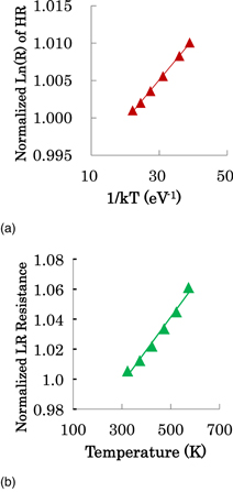
Fig. 3. (Color online) (a) Natural Log of resistance versus 1/kT plot of the HR resistor. (b) Resistance versus temperature T plot of the LR resistor.
Download figure:
Standard image High-resolution image3.2. Resistance stability evaluation and model
The bias temperature stress test can be used to monitor the stability of interconnects or resistor structures. 29) Resistance stability tests of LR and HR were performed using low current (Low_I ∼ 2 mA) and high current (High_I ∼ 8 mA) stress levels at 150 °C, as shown in Fig. 4. Both HR and LR samples showed high stability with minimal change in resistance under Low_I stress. LR had a very small Rshift of <0.02%. The Rshift of HR increased to 0.2% and then saturated. Under High_I stress, LR still exhibited high stability with a minimal change of 0.1%, whereas HR displayed a power-law increment of 4% at the end of the test.
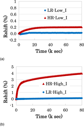
Fig. 4. (Color online) Resistance shift of the HR and the LR poly-Si resistors versus stress time under (a) low current and (b) high current stress condition at 150 °C.
Download figure:
Standard image High-resolution imageThe resistance shift (%) observed at different temperature steps during the stability test is shown in Fig. 5. The stress currents are turned on in step (2). When the stress current is turned off in step (3) and when the temperature returns to the initial value of 25 °C, the resistances of HR and LR under Low_I stress recover to their initial values at this temperature. Only HR under High_I stress has a permanent resistance shift after the stress current turned off in step (4), as shown in Fig. 5(b). Based on these stability stress results, a new resistance stability model that can explain the time dependences under low and high stress levels needed to be developed.

Fig. 5. (Color online) (a) Temperature profile of the stability test steps. (a) The resistance shift of the LR and the HR at each stability test step. Only the HR under High_I stress has a permanent resistance shift after the test at the initial temperature of 25 °C.
Download figure:
Standard image High-resolution imageA critical stress current to make a permanent resistance increment is observed in the interconnect metal structure due to electromigration. 30,31) Electromigration is defined as the migration of atoms of conduction line due to the momentum exchange owing to collisions with conduction electrons. 32) A void or hillock of the conduction line may occur due to the nonuniformities of atom migration induced by defects in the lattice or the grain structure. 33–36) The PMOS FET results in permanent degradation and induces recovery effects under NBTI stress. 37) NBTI degradation is primarily due to carrier trap generation and its recovery effect can be explained as the de-trapping of trapped carriers in the absence of stress. 38,39) The carrier-trapping model was proposed to explain the electrical transport properties of poly-Si at different dopant concentrations. 8)
Reviewing the aforementioned degradation models, we developed a novel carrier-trapping model for the poly-Si resistance shift evolution. Under stress, the carriers gain energy to overcome the barrier and are confined to the trap sites. However, new traps are also generated as a result of stress. The available trap density, Dt, which is time (t) dependent, can be defined as follows:

where Dt(0) is the initial available trap density and Dts is the stress induced new trap density, and Nt is the trap site density occupied by the carrier.
The trap occupation rate is assumed to be proportional to the available trap density Dt, with rate constant ra

If the stress condition is low and Dts can be ignored, Nt can be derived as an exponential function of t.


Conductivity σ is assumed to be proportional to the carrier density Na(t), and σ can be derived as
where Na'(0) ≡ Na(0)−Dt(0).
Given that resistance R is proportional to the inverse of the conductivity and Rshift under evaluation is  1, we suppose that Na(t)
  Dt and Na'(0)
  Dt(0), and derive Rshift(t) as follows:


The physical meaning of Eq. (12) is that the resistance shift increases exponentially and has a saturation point given by the ratio of initially available trap density to the total carrier density, because the number of available trap sites is limited. This ratio was 0.2% for HR, as shown in Fig. 4(a).
Under high-stress conditions, the new trap density is assumed to be larger than the occupied trap density. Assuming that Dts increases as a power law with time under such conditions, Nt of Eq. (4) will also exhibit a power-law time dependence


where rate constant rs and exponent n are related to the test structure and stress conditions. Rshift(t) under a high-stress condition is then derived as follows:


Rshift in Eq. (17) increases as a power law with time and is proportional to the ratio of the occupied trap density to the initial carrier density.
LR exhibits higher stability under the same stress current levels, as shown in Fig. 4. This implies that the generation of new LR carrier traps requires a higher stress current. The resistance stability models of Eqs. (12) and (17) predict that resistance will increase with different time dependences according to the different stress conditions. These models successfully explain the data of the poly-Si Rshift of HR and fit them well, as shown in Fig. 6. For the medium-stress condition, the time dependence of Rshift is a transition function between Eqs. (12) and (17).

Fig. 6. (Color online) Model fitting results of resistance shift of the HR with respect to time for low and high stress currents according to Eqs. (12) and (17).
Download figure:
Standard image High-resolution image3.3. Stability lifetime evaluation and model
Stability tests with higher constant stress currents at higher temperatures were performed to clarify the current and temperature effects on ploy-Si resistance shifts, as shown in Figs. 7 and 8. The test oven temperatures were 250 °C–300 °C, and the sample temperature was estimated using the resistance and temperature relation shown in Fig. 2(b). The stress currents of HR and LR were approximately about 1.5 and 1.8 times the values of High_I respectively. Under these high-stress conditions, more trap sites may be generated, and both HR and LR exhibited power-law Rshift increments, as expected.
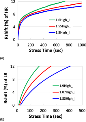
Fig. 7. (Color online) Resistance shift of (a) the HR and (b) the LR poly-Si resistors at different stress currents to evaluate the lifetime.
Download figure:
Standard image High-resolution image
Fig. 8. (Color online) Resistance shift of (a) the HR and (b) the LR poly-Si resistors at different stress temperatures for to evaluate the lifetime.
Download figure:
Standard image High-resolution imageIn general, stress time when catastrophic failure occurs is defined as the time to failure (TTF) of a metal line under electromigration stress. 40,41) A stability lifetime or TTF may be defined as the time at which Rshift reaches a specific criterion for more reliable resistance control. Based on this definition and the results of Figs. 7 and 8, a stability TTF model can be developed to predict other TTFs under different stress conditions. To demonstrate the TTF model, we adopted a 4% resistance change as the TTF criterion for the poly-Si resistors, which is the maximum resistance shift in Fig. 4(b). The TTF results for different stress currents and temperatures show that Ln(TTF) has a linear dependence on 1/T and stress current, as shown in Fig. 9. Based on these TTF results, we utilized the free energy of activation approach for the stress-induced Rshift model. 42) According to this approach, a reaction rate Kr is related to the free energy of activation G which is a sensitive function of stress parameters (electrical current I in this study) as follows:


where Ea is the activation energy and n is the acceleration factor of the stress current. 43) Given that the TTF is inversely related to the reaction rate, we proposed the time to failure of the poly-Si resistor as follows:

Based on the free energy model of Eq. (20), Ln(TTF) has linear a dependence on I and 1/T, as demonstrated in Fig. 9. The Ea of LR and HR are found to be 1.9 and 0.78 eV, respectively. A high-resistivity poly-Si resistor was reported to have Ea of 0.68 eV, consistent with that of HR found here. 21) The grain or lattice migration energy is larger than the GB migration energy. 44–47) The disorder at GBs in polycrystalline silicon allows for high-diffusivity paths along which dopant atoms can easily move. If the carrier trap site generation is related to the migration of atoms or dopants, an HR with GB conduction is expected to have a lower Ea than that of LR with grain conduction. This expectation is consistent with the Ea results obtained using the proposed free energy model. The n values of LR and HR were 3.0 and 11.4 cm2 MA−1, respectively. A higher n of HR implies a more severe TTF decrement when the operation current increases for HR poly-Si resistors. We estimated the TTF of the HR under the lower stress condition of Fig. 4(a) using Eq. (20), as shown in Fig. 10. This result shows that the free energy TTF model can serve as a reliable stability model for evaluating the long-term performance of poly-Si resistors.
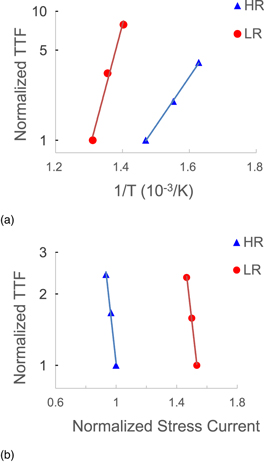
Fig. 9. (Color online) The TTF of poly-Si resistors versus (a) 1/T and (b) stress current plot showing the exponential dependence of TTF on 1/T and the current. Both vertical axes are in logarithmic scale.
Download figure:
Standard image High-resolution image
Fig. 10. (Color online) TTF predicted by the model proposed in this study fit well with the TTF data at low-stress conditions.
Download figure:
Standard image High-resolution image3.4. TLP robustness evaluation and model
The TLP test can be used to assess the robustness of the resistor under a pulse current at high power. TLP current pulses with different pulse widths were applied to the HR and LR poly-Si resistors in this study. The critical failure current, Ifail, was defined as the TLP current that caused the breakdown of the resistor. Ifail exhibited different TLP time width, tw, dependence as shown in Fig. 11(a) with Ifail 2 as the vertical axis and 1/tw as the horizontal axis. Ifail decreased as the pulse time width increases, and started to saturate when tw was larger than 1 μs.
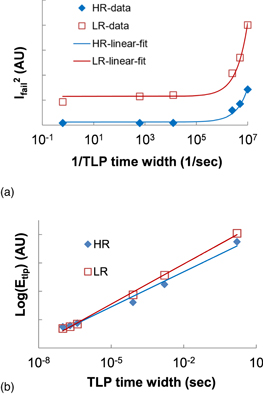
Fig. 11. (Color online) (a) Square of the TLP critical failure current (Ifail) and (b) TLP energy (Etlp) during the breakdown pulse step verse pulse width plots of the LR and the HR poly-Si resistors. The solid lines are the linear fitting lines.
Download figure:
Standard image High-resolution imageThe correlation between Ifail and tw involves the breakdown energy (Eb) and conduction energy during the TLP test. When breakdown happens during a TLP pulse step, the total TLP input energy, Etlp, includes Eb of resistor and the thermal conduction energy as follows:


where ΔT is the temperature difference between the resistor and environment and kc is the thermal conductance.
When tw is smaller than the thermal time constant of the resistor, the heat energy dissipated from the resistor to the environment by conduction is negligible, and the TLP breakdown process can be regarded as adiabatic. Under such conditions, Eq. (22) can be simplified as follows:

Under the adiabatic conditions of Eq. (23), Ifail 2 is proportional to 1/tw. The linear fitting lines of Ifail 2 versus 1/tw (solid lines) are shown in Fig. 11(a). The fitting results are very good in the range of small tw values.
When tw increases and exceeds the thermal time constant of the resistor, Ifail first decreases and eventually saturates to the square root of kc·∆T/R [Fig. 11(a)], according to Eq. (22).
Given that the resistance of LR is lower than that of HR, Ifail of LR will be larger than that of HR if the Eb and kc of these two resistors are similar, according to Eq. (22). This conclusion is validated by the Ifail results for HR and LR, as shown in Fig. 11(a). The TLP input energy for breakdown increases as tw increases according to Eq. (21), which is confirmed by the TLP test results in Fig. 11(b). Given that the TLP energy approaches the value of Eb as tw decreases, the TLP energies in the small tw range in Fig. 11(b) also confirm that the Eb values of LR and HR are similar.
Based on the proposed TLP breakdown model, the specification of the pulse current for the poly-Si resistor can be accurately defined with different pulse time widths. Because Ifail of LR is higher than that of HR, the LR poly-Si resistor can sustain a larger pulse current than the HR poly-Si resistor during electrostatic discharge or electrical overstress events. SEM images of the silicide-block LR poly-Si resistors after low current stability stress tests did not depict significant failure in our previous study, as shown in Fig. 12(a). 20) When the stress current was larger than the breakdown current, the observed failure sites of the silicide poly-Si resistor were usually near the contact area, where the current crowding and heat generation were severe, as shown in Fig. 12(b).

Fig. 12. SEM images of (a) a silicide-block LR poly-Si resistor after low current stress and (b) a silicide poly-Si resistor after breakdown current stress.
Download figure:
Standard image High-resolution image
4. Conclusions
The temperature and voltage dependences of resistance are distinctly different for poly-Si resistors with different dopant concentrations. Intra-grain and grain boundary resistance mechanisms were proposed to contribute to the resistance of poly-Si thin-film resistors in this study. A highly doped poly-Si resistor with low resistance has higher stability and is more robust than a lightly doped resistor when considering the operation current.
A novel resistance shift model based on carrier trapping and trapping generation was proposed to explain the resistance shift property of poly-Si thin-film resistor for different stress currents successfully. A free energy model of the stability TTF of poly-Si was developed to explain the current and temperature dependence property and to accurately estimate the TTF under lower stress conditions. A breakdown model involving heat conduction was proposed for the evaluation of the TLP robustness of the poly-Si resistors. This model successfully explained the dependence of the breakdown current on TLP time width and facilitated the specification of the critical pulse current of a poly-Si resistor.