
Abstract
We have investigated the memory characteristics of InGaZnO (IGZO)-channel ferroelectric FETs (FeFETs) with 2D planar and 3D structures by TCAD simulation to improve the memory window (MW) with a floating-body channel for high-density memory applications. From the study on 2D planar FeFETs with a single gate and a double gate, the MW depends on channel length (L) and is enhanced with shorter L due to stronger electrostatic coupling from the source and drain to the center region of the IGZO layer. From the study on 3D structure FeFETs with macaroni (MAC) and nanowire (NW) structures, a large MW can be obtained especially in NW FeFETs due to the electric field concentration by Gauss's law in the 3D electrostatics. Furthermore, we have systematically studied and discussed the device design of MAC and NW structure FeFETs in terms of the diameter and thickness for high-density memory applications. As the IGZO thickness and the outer diameter of the IGZO layer decrease, the MW increases due to the voltage divider and the electric field concentration. The device parameters that can maximize the MW can be determined under the constraints of the layout and material based on this study.
Export citation and abstract BibTeX RIS

Content from this work may be used under the terms of the Creative Commons Attribution 4.0 license. Any further distribution of this work must maintain attribution to the author(s) and the title of the work, journal citation and DOI.
1. Introduction
In a cyber-physical society, a tremendous amount of data is collected by edge devices, and stored and processed by cloud servers. It is important to make full use of such big data to create innovative social services. However, it is often reported that the amount of available data at edge devices largely exceeds the data traffic around data centers. This gap is increasing and thus the role of edge devices will become more important. We think that edge devices will be required to have high-capacity yet low-power memory not only for storage but also for enabling edge AI computing such as machine learning.
As for high-capacity storage memory, NAND flash memory is the most cost-effective and the mainstream in the market. However, its power consumption and operation speed can be obstacles for edge devices that operate under the constraints of power supply. A ferroelectric FET (FeFET) is a one-transistor memory device that has a ferroelectric gate insulator in a FET structure. 1,2) A FeFET realizes high threshold voltage (Vth) and low Vth by the direction of the ferroelectric polarization which can be switched by the gate voltage (Vg). A FeFET operates at low power and high speed due to its field-driven write operation. Since the discovery of CMOS-compatible ferroelectric HfO2 (FE-HfO2), the FeFET has attracted much attention for high-capacity memory applications. 3–6)
NAND flash memory has migrated to a 3D vertical stack structure due to scaling challenges and the increasing demand for higher density. 7–10) The same architecture is applicable to FeFETs. In fact, a 3D vertical FeFET with FE-HfO2 has been demonstrated with a poly-Si channel. 11,12) However, several challenges with the poly-Si channel have been raised regarding performance, reliability and low-voltage operation. 13) Poly-Si may suffer from low mobility especially at an ultrathin film less than 10 nm due to the grain boundary and defects inside the grain. 14) A low-k interfacial layer is inevitably formed between the FE-HfO2 layer and the poly-Si layer, which causes reliability degradation by charge trapping and prevents low-voltage operation due to the large voltage drop at the interfacial layer. 12)
Oxide semiconductors such as InGaZnO (IGZO) have been developed for flat-panel display applications, 15–18) and have been proposed as an alternative channel material to poly-Si for FeFETs 19,20) [Fig. 1(a)]. IGZO-channel FeFETs may solve these challenges by their high mobility and the lack of low-k interfacial layer formation between an FE-HfO2 layer and an IGZO layer. 21–24) One key challenge of IGZO-channel FeFETs is their weak erase operation, 19) which is a similar situation to that of 3D NAND flash memory. IGZO is an n-type channel material and a FET with an IGZO channel is an n-type junctionless transistor. Since minority carrier holes are hardly generated in IGZO, the body potential is not fixed but floating, and the ferroelectric polarization charge is not balanced with the charge in the IGZO layer during the erase operation. 24) Thus, the erase operation is not efficiently done [Fig. 1(b)]. Although it is known that a 3D structure facilitates the write operation in 3D NAND flash memory, 25,26) the impact of a 3D structure on 3D FeFETs has not been fully discussed yet.

Fig. 1. (Color online) (a) A schematic of a 3D vertical stack FeFET with an IGZO channel. (b) An illustration of the challenge of weak erase operation in a 3D vertical IGZO-channel FeFET.
Download figure:
Standard image High-resolution imageTo address the issue of the erase operation in IGZO-channel FeFETs and improve the memory window (MW), in this work, we study the memory characteristics of IGZO-channel FeFETs with 2D planar and 3D structures by TCAD simulation. We simulate single-IGZO FeFETs instead of actual series-connected transistors with the source and drain terminated at the end of the NAND string. In the 3D vertical architecture, each IGZO FeFET is an n-type junctionless transistor and connects to the source and drain in the string by applying pass voltage on the gates of the other series-connected transistors. Therefore, the study of single-IGZO FeFETs is relevant and applicable to the study of 3D vertical architecture. This paper is an extended version of short conference proceedings 27) including a detailed analysis and an entirely new section on a parametric simulation study on 3D structure FeFETs to provide device design guidelines for high-density memory applications.
2. Simulation methods
We previously built a TCAD model for 2D planar FeFETs 28–30) with IGZO channels 19,24,27) which captured the essential physics and qualitatively reproduced the measurement results with the basic material parameters of FE-HfO2 (HfZrO2, HZO) and IGZO. In this work, we extend our TCAD model from a 2D planar to a 3D structure. As shown in Fig. 2, we simulated (a) single-gate (SG) planar FeFETs with a floating body, (b) double-gate (DG) planar FeFETs corresponding to FinFETs or nanosheet FETs, (c) macaroni (MAC) structure FeFETs similar to 3D NAND flash memory, and (d) nanowire (NW) structure FeFETs. For the MAC FETs, the inner core was filled with SiO2. All devices were junctionless transistors with ohmic contact at the source and drain. The source and drain contacts were put on the side surface of the IGZO region and were aligned to the edge of the gate. The remanent polarization charge density (Pr) and the coercive field (Ec) of HZO were 23 μC cm−2 and 1.16 MV cm−1, respectively. To focus on the static characteristics, dynamic model parameters were not taken into account. The bandgap and the carrier concentration of IGZO were 3.2 eV and 1019 cm−3, respectively. Note that the ferroelectric thin film was modeled as a continuous medium and shows non-uniform ferroelectric polarization 30) in this work. The HZO thickness (tHZO) was 10 nm, which is a practical value ensuring high ferroelectricity and low leakage current. The IGZO thickness (tIGZO) and the NW diameter (dIGZO) were fixed at 8 nm for the channel length (L) dependence in section 3.1. These parameters were varied for the study on the device design of MAC and NW FeFETs for different outer diameters (D) of the IGZO channel in the MAC and NW structures in section 3.2. These device parameters are depicted in Fig. 2. For the write operation, a bidirectional DC Vg sweep (±5 V) was applied, where 5 V is the program voltage and −5 V is the erase voltage. The MW was defined by taking the difference between the high Vth after erase and the low Vth after the program.
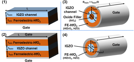
Fig. 2. (Color online) Schematics of the device structures simulated in this work: (a) SG planar, (b) DG planar, (c) MAC, and (d) NW.
Download figure:
Standard image High-resolution image3. Results and discussion
3.1. Channel length (L) dependence of 2D planar and 3D structure FeFETs
First, we simulated SG planar FeFETs varying L. The simulated drain current (Id) versus Vg curves are shown in Fig. 3. As L decreases, the MW rapidly increases in the sub-100 nm L region, while the short channel effect (SCE) is degraded with a large subthreshold swing. To discuss this L dependence of the MW, Fig. 4 shows the electrostatic potential and the polarization charge density for L = 100 nm and L = 30 nm in the erase state. In the case of long L, the electric field from the gate is concentrated near the source and drain. However, the center region of the IGZO layer is floating and the electric field from the gate is sparse. Thus, it is difficult to apply high voltage on the HZO layer and induce polarization switching around the center region of the HZO layer. In the case of short L, on the other hand, the regions where the electric field concentrates near the source and drain merge around the center of the IGZO layer. In other words, the source and drain electrostatically couples to the center region of the IGZO layer. Thus, the large electric field is applied on the HZO layer and polarization switching occurs even around the center region of the HZO layer. Such electrostatic coupling from the source and drain also gives rise to the SCE. Please note that some hump behavior is seen in the reverse sweep in Fig. 3. The IGZO FeFET is a junctionless transistor, which has body conduction near the flat-band region and surface conduction in the accumulation region. In our simulation conditions, after the surface channel is turned off, the body conduction near the top surface is not pinched off until sufficiently high negative Vg is applied. This leads to hump behavior.
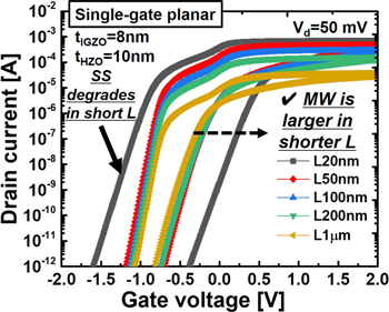
Fig. 3. (Color online) The simulated Id–Vg curves of the SG planar FeFETs with varying channel length (L) at Vd = 50 mV.
Download figure:
Standard image High-resolution image
Fig. 4. (Color online) The simulated (a) electrostatic potential and (b) ferroelectric polarization charge density (perpendicular to the channel) for L = 100 nm and 30 nm.
Download figure:
Standard image High-resolution imageNext, we simulated DG planar FeFETs varying L. The simulated Id–Vg curves are shown in Fig. 5. The MWs of the SG FeFETs and the DG FeFETs are plotted against L in Fig. 6. The DG planar FeFETs show larger MWs with less SCE than the SG planar FeFETs. The DG structure can control the IGZO-body potential from both sides of the gate. Even though polarization switching only occurs near the source and drain in the erase operation as in the SG planar FeFETs, the DG FeFETs can efficiently cut off the channel as shown in the electrostatic potential in Fig. 7, and thus realize high Vth in the erase operation and the large MW.

Fig. 5. (Color online) The simulated Id–Vg curves of the DG planar FeFETs with varying L at Vd = 50 mV.
Download figure:
Standard image High-resolution image
Fig. 6. (Color online) The extracted MWs of the SG planar FeFETs and the DG planar FeFETs.
Download figure:
Standard image High-resolution image
Fig. 7. (Color online) The simulated ferroelectric polarization charge (perpendicular to the channel) and electrostatic potential for (a) a DG planar FeFET and (b) an SG planar FeFET.
Download figure:
Standard image High-resolution imageThen, we simulated MAC FeFETs and NW FeFETs varying L. The simulated Id–Vg curves are shown in Figs. 8(a) and 8(b) for the MAC FeFETs and the NW FeFETs, respectively. The MWs of the MAC and NW FeFETs are plotted against L in Fig. 9, where both FeFETs show large MWs compared to the SG FeFETs and the DG FeFETs. In particular, the NW FeFETs show the largest MWs for the entire L regions. There is much less L dependence in the NW FeFETs than in the other FeFETs. To understand such memory characteristics of the NW FeFETs, the NW diameter dependence of the Id–Vg curves is studied. As shown in Fig. 10, the MW increases as the NW diameter decreases. This is mainly attributed to the electric field concentration in the 3D cylinder structure. In the NW structure, given Vg, the electric field is concentrated toward the inside of the HZO layer by Gauss's law. The larger MW in the NW FeFETs than in the MAC FeFETs is due to the smaller D in the NW FeFETs while tHZO is the same for both FeFETs. The ratio of the inner surface area to the outer surface area of the HZO layer is lower in the NW FeFETs and thus the electric field is more concentrated in the NW FeFETs. The simulated polarization charge density along the channel direction in an NW FeFET is shown in Fig. 11(a), in which polarization switching occurs in the entire HZO layer in the erase operation. Figure 11(b) shows the electric field in the diameter direction, which clearly illustrates the electric field concentration.
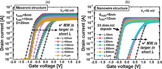
Fig. 8. (Color online) (a) The simulated Id–Vg curves of the MAC FeFETs with varying L at Vd = 50 mV. (b) The simulated Id–Vg curves of the NW FeFETs with varying L at Vd = 50 mV.
Download figure:
Standard image High-resolution image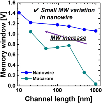
Fig. 9. (Color online) The extracted MWs of the MAC FeFETs and the NW FeFETs.
Download figure:
Standard image High-resolution image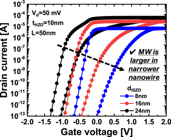
Fig. 10. (Color online) The simulated Id–Vg curves of the NW FeFETs with L = 50 nm, and with D = 24 nm, 16 nm, and 8 nm, at Vd = 50 mV.
Download figure:
Standard image High-resolution image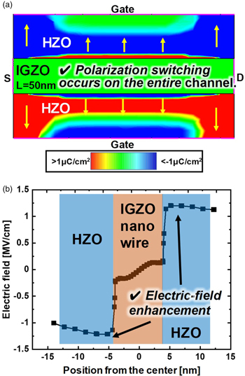
Fig. 11. (Color online) (a) A cross-sectional view of the simulated ferroelectric polarization (vector component) in the diameter direction of the NW in the erase state. (b) The extracted electric field in the diameter direction of the NW in the erase state.
Download figure:
Standard image High-resolution image3.2. Diameter (D) and IGZO thickness (tIGZO) dependence of MAC and NW FeFETs
The actual design of 3D vertical FeFETs depends on available process technologies and layout constraints to achieve a high-aspect-ratio trench and high-density integration. In this section, we systematically investigate the diameter and IGZO thickness dependence of MAC and NW FeFETs to explore device design guidelines. RIGZO is defined by tIGZO/D to express the volume ratio of the IGZO layer to the total diameter. MAC FeFETs have RIGZO < 0.5 and NW FeFETs have RIGZO = 0.5. The tHZO is fixed at 10 nm, which is a practical value ensuring high ferroelectricity and low leakage current. L is 50 nm, which is also a relevant value to 3D NAND flash memory and avoids severe SCE as seen in the previous section. Note that L is defined by the deposition thickness of the gate in a 3D vertical stack structure and thus determined by the process integration. Figures 12(a)–12(c) show the simulated Id–Vg curves with D = 24 nm, 16 nm, and 8 nm, with varying RIGZO, respectively. The narrower FeFETs show lower on-current due to the smaller effective channel width. Figures 13(a) and 13(b) summarize the extracted MWs versus RIGZO and tIGZO, with varying D, respectively. At RIGZO = 0.5, which is the case of the NW FeFETs, the MW largely increases as D decreases. This is the same result in Fig. 10 attributed to the 3D electric field concentration. In addition, as RIGZO decreases, the MW monotonically increases. This is mainly due to the voltage divider between the HZO layer and the IGZO-channel layer. As tIGZO decreases, more voltage drops on the HZO layer. For D = 8 nm, the RIGZO dependence is relatively weak because the 3D electric field concentration with small D is more dominant than the voltage divider with a thin IGZO layer. These trends are more clearly seen in Fig. 13(b). In the MAC FeFETs, the MWs follow almost the same trend as a function of tIGZO even with different D values because of the voltage divider between the HZO layer and the IGZO channel. The NW FeFETs deviate from this universal trend because of the 3D electric field concentration effect, which depends on D.
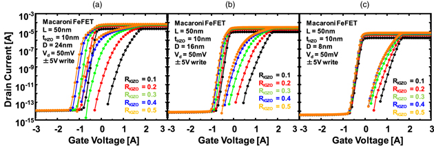
Fig. 12. (Color online) The simulated Id–Vg curves of the MAC FeFETs with L = 50 nm, and with (a) D = 24 nm, (b) 16 nm, and (c) 8 nm, with varying RIGZO (= tIGZO/D). A MAC FeFET with RIGZO = 0.5 is an NW FeFET.
Download figure:
Standard image High-resolution image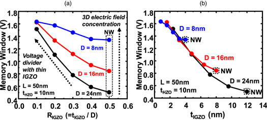
Fig. 13. (Color online) (a) The extracted MW versus RIGZO of the MAC FeFETs with L = 50 nm, and with D = 24 nm, 16 nm, and 8 nm. (b) The extracted MW versus tIGZO of the MAC FeFETs with L = 50 nm, and with D = 24 nm, 16 nm, and 8 nm.
Download figure:
Standard image High-resolution image
From the device design point of view, once the diameter of the deep trench in a 3D FeFET is decided from the density and layout requirement, then D, which is the total diameter including the IGZO channel and the filler, is determined at the given HZO thickness. Next, the IGZO thickness is chosen for the target MW. An extremely thin IGZO thickness may be required in the regime of MAC FeFETs. If the IGZO thickness is too thin to conformally deposit inside a deep trench of a high aspect ratio and filler deposition is technically difficult, making NW FeFETs by entirely filling the trench with IGZO is a feasible approach. NW FeFETs can facilitate the process integration and boost the MW by the 3D electric field concentration.
4. Summary
We simulated the memory characteristics of IGZO-channel FeFETs with 2D planar and 3D structures by TCAD simulation to study MW improvement with a floating-body channel for high-density memory applications. From the study on 2D planar devices with SG and DG structures, the MW depends on L and is enhanced with shorter L, which is due to strong electrostatic coupling from the source and drain to the center region of the IGZO layer. From the study on the 3D structure FeFETs with MAC and NW structures, a large MW can be obtained especially in the NW structure due to the electric field concentration by the 3D electrostatics. MAC FeFETs and NW FeFETs were simulated by systematically varying the parameters of D, RIGZO and tIGZO. The MW can be improved by the 3D electric field concentration in a narrow outer diameter of the IGZO layer and a voltage divider with a thin IGZO-channel layer. These findings are useful for designing 3D vertical FeFETs for high-density memory applications.
Acknowledgments
This work was supported by JST CREST (16815651), JSPS KAKENHI Grant No. JP18H01489, and Tokyo Electron Ltd. and TSMC Advanced Semiconductor Research Project.