

Abstract
van der Waals heterostructures (vdWHs) based on atomically two-dimensional materials have gained extensive attention due to their great potential in the new era of next-generation optoelectronics. Most reported photodetectors exhibit type-II band alignment and their photodetection performance is often limited by either low photoresponsivity or high dark current. However, type-Ⅲ vdWHs with broken gaps are still very rare, which limits the development and application of two-dimensional (2D) materials in the fields of photodetector. Here, we demonstrate a highly sensitive black phosphorus (BP)/SnS2 photodetector with type-III (broken-gap) band alignment. The dark current of BP/SnS2 vdWH is greatly suppressed by high barrier at the junction and high photoresponsivity generated from high tunneling current when illuminated. The BP/SnS2 vdWH exhibits both ultrahigh photodetectivity of 6.72 × 10¹² Jones and photoresponsivity of 295.3 A W−1 under the illumination of 365 nm light (0.53 mW cm−2). Our results provide an avenue for developing high performance optoelectronics and better understanding the underlying physics in the broken-band alignment systems.
Export citation and abstract BibTeX RIS
1. Introduction
van der Waals heterostructures (vdWHs) based on atomically two-dimensional materials have great potential in the next generation of electronics and optoelectronic devices due to its wide variety of materials and the ultrathin morphology features. 1–3) The library of 2D materials makes it possible to design heterostructures by integrating proper material properties. Among them, black phosphorus (BP) has been studied as a promising candidates for future photodetection applications due to BP possess layer-dependent gap direct bandgaps (from 0.3 eV for bulk to 2.0 eV for monolayer), high carrier mobility (up to 1000 cm2 V−1 s−1), and large coverage detection range. 4–6) In addition, tin disulfide (SnS2) is a promising candidate for field effect transistors (FETs), 7) logic circuits, 8,9) and photodetectors 10,11) because of its appropriate indirect bandgap (2.08–2.44 eV), high optical absorption coefficient exceeding 104 cm−1, and large on/off ratio (>106).
In general, three types of band alignments can be distinctly classified when different 2D materials are stacked together, including: straddling gap (type-I),
12) staggered gap (type-II)
13,14) and broken-gap (type-III).
15–17) Thus far, most reported photodetectors have been realized with type-II band alignment to utilize the excellent electron–hole pair separation ability in heterostructures.
18) However, the photodetectivity of photodetectors is typically limited by either low photoresponsivity or a high dark current.
19,20) For example, photovoltaic device based on BP/MoS2 vdWHs can reach a high  ratio of ≈103, while the photoresponsiviy is only ≈1 m W−1.
21) Recently, tunneling field effect transistors (TFETs) based on type-Ⅲ vdWHs have shown great potential in the field of low-power optoelectronic devices due to their low OFF-state current, which may exhibit excellent performance in photodiodes.
22–24)
ratio of ≈103, while the photoresponsiviy is only ≈1 m W−1.
21) Recently, tunneling field effect transistors (TFETs) based on type-Ⅲ vdWHs have shown great potential in the field of low-power optoelectronic devices due to their low OFF-state current, which may exhibit excellent performance in photodiodes.
22–24)
In this work, we report a high photodetectivity and photoresponsivity photodetector based on a BP/SnS2 vdWHs. The BP/SnS2 vdWHs shows strong interlayer coupling verified by Raman, which promotes highly efficient charge transfer in the channel. Thus, the BP/SnS2 vdWHs exhibits ultrahigh photodetectivity of 6.72 × 10¹² Jones ( ratio of ≈2 × 10³) and high photoresponsivity of 295.3 A W−1. The dark-carrier tunneling was highly suppressed by the depletion region of the junction whereas the photocarrier tunneling was efficiently improved by the high direct tunneling (DT) current when illuminated, which has been confirmed by the energy band structures and electrical characteristics fitted with DT. The experiments demonstrate that BP/SnS2 vdWHs possess type-III (broken-gap) band alignment, indicating their application in TFETs devices and low-power photodetector.
2. Experimental section
2.1. Device fabrication
The BP/SnS2 heterostructure device was fabricated on the SiO2/Si substrate by using a dry transfer technique in a glove box. The few-layer flakes of BP and SnS2 were mechanically exfoliated from commercially bulk crystal (the Six Carbon Technology Corporation) using scotch tape. Firstly, the thin SnS2 flakes were mechanically exfoliated on a highly p-doped Si substrate with a 300 nm thick SiO2 layer. Then, the same method was adopted for transferring few layers BP onto the SnS2 under the optical microscope assisted by at aligned transfer system. Finally, to fabricate the heterostructure device, the electrode patterns were produced by electron-beam lithography system (EBL, Raith eLINE Plus) and Cr/Au (10 nm/50 nm) metals were deposited by electron-beam evaporation (Ei-5z) to fabricated source and drain electrodes.
2.2. Device characterization
The Raman scattering measurements (LABRAM HR, Japan Horriba-JY) were performed at room temperature using a 532 nm laser as the excitation source. Electrical characteristics of the heterostructure device were conducted with two semiconductor characterization source meters (Keithley 2612B and 2400). For photodetection, the photoresponsivity was measured using a commercial laser source with an illumination wavelength of 365 nm (UVEC-4 II, SHENZHEN LAMPLIC TECH CO, LTD).
3. Results and discussion
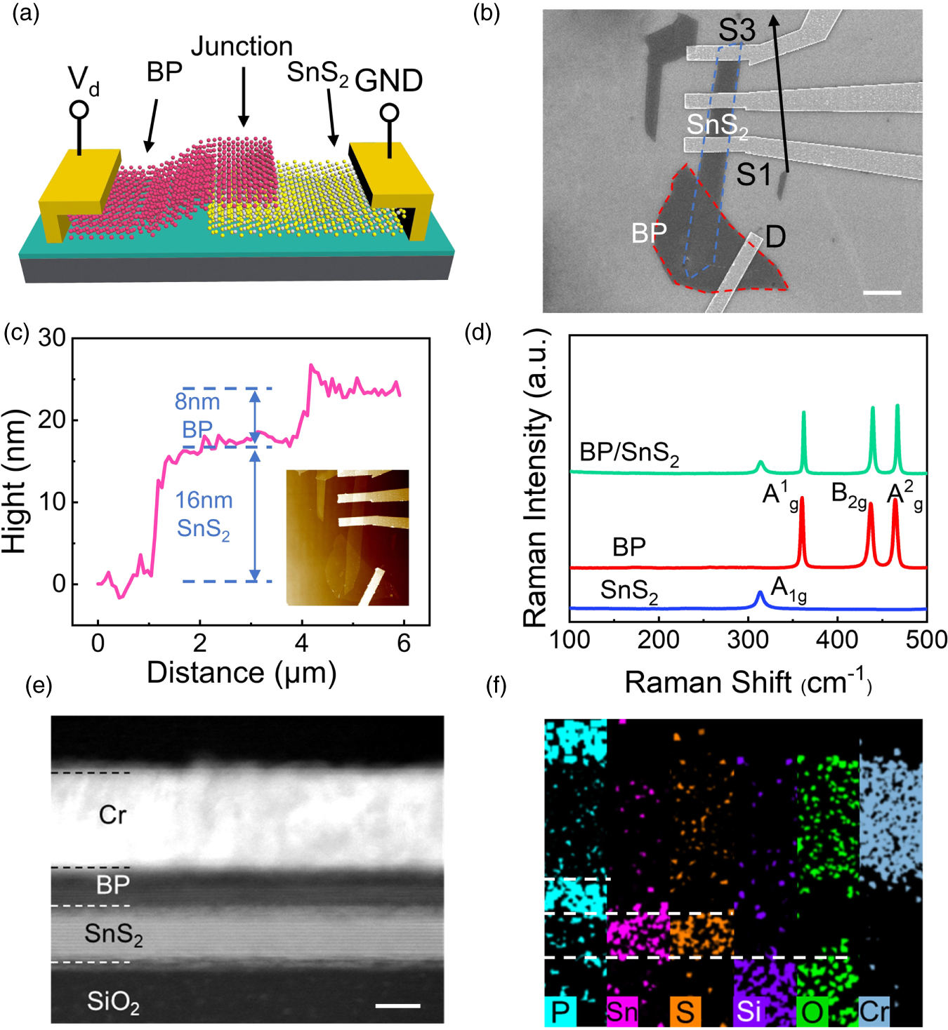
Figure 1(a) shows a schematic illustration of the BP/SnS2 heterostructure device. Few layers p-type BP and n-type SnS2 flakes, mechanically exfoliated from their bulk materials, were transferred onto a 300 nm SiO2/Si substrate. Figure 1(b) presents a typical scanning electron microscopy image of the heterostructure device. Multiple metal electrodes were fabricated on the top of BP and SnS2 regions by EBL and subsequent deposition of 10 nm/50 nm Cr/Au. As shown in Fig. 1(c), the thicknesses of the BP and SnS2 flakes were determined to be 8 nm and 16 nm by atomic force microscopy, respectively and the inset shows the surface morphology. The Raman spectra of BP/SnS2 heterostructure and isolated BP and SnS2 was shown in Fig. 1(d). For the isolated BP region, the BP shows three dominant peaks at  (436.5 cm−1),
  (358.8 cm−1) and
  (463.7 cm−1), which is consistent with previous studies.
11,25) While for the isolated SnS2 region, the SnS2 shows one main peak at
(463.7 cm−1), which is consistent with previous studies.
11,25) While for the isolated SnS2 region, the SnS2 shows one main peak at  (313.4 cm−1). All these peaks are contained in the spectra of BP/SnS2 overlapped region, indicating the successful formation of BP/SnS2 heterostructure. Figures 1(e), 1(f) is the transmission electron microscopy (TEM) imaging and the energy dispersive X-ray specteometry (EDS) elemental mapping of the heterostructure of the device. According to the TEM imaging, the interface of all layers is clear and flat. Furthermore, the EDS analysis of O elements demonstrates that the BP/SnS2 heterostructure is not oxidized. In order to prevent the oxidation of BP, Liu' group synthesized the Te-doped and S-doped BP, which change the conduction band minimum (CBM) shifting close to the redox potential of O2/O2
−, and suppresses the oxidation process of BP.
6,26)
(313.4 cm−1). All these peaks are contained in the spectra of BP/SnS2 overlapped region, indicating the successful formation of BP/SnS2 heterostructure. Figures 1(e), 1(f) is the transmission electron microscopy (TEM) imaging and the energy dispersive X-ray specteometry (EDS) elemental mapping of the heterostructure of the device. According to the TEM imaging, the interface of all layers is clear and flat. Furthermore, the EDS analysis of O elements demonstrates that the BP/SnS2 heterostructure is not oxidized. In order to prevent the oxidation of BP, Liu' group synthesized the Te-doped and S-doped BP, which change the conduction band minimum (CBM) shifting close to the redox potential of O2/O2
−, and suppresses the oxidation process of BP.
6,26)

Fig. 1. (Color online) Device structure and morphology properties of BP/SnS2 vdWHs. (a) Schematic diagram of the BP/SnS2 heterostructure on a SiO2/Si substrate. (b) The SEM image of the heterostructure, where the scale bar is 5 μm. Electrodes S1–S3 are the source electrodes in contact with SnS2, and D is the drain electrodes in contact with BP. The source electrode connects to the ground (GND), and the bias voltage is applied on the drain electrode. (c) Height profile along the white line, which indicates the thicknesses of the top (BP) and bottom (SnS2) layers, respectively. The inset shows a topographic AFM image of the BP/SnS2 device. (d) Raman spectra of the isolated BP, isolated SnS2, and their overlapped regions. (e) Transmission electron microscopy (TEM) imaging of the heterostructure is in order with BP/SnS2/SiO2 layers. The interface of all layers is clear, flat and not oxidized. (f) Energy dispersive X-ray spectroscopy (EDS) elemental mapping of P, Sn, S, Si, O and Cr, corresponding to Cr/BP/SnS2/SiO2 layers in the TEM imaging.
Download figure:
Standard image High-resolution imageIn order to quantitatively probe the charge transfer at the heterostructure, we measured a series of electrical characteristics in the same device. Figures 2(a), 2(b) shows the transfer characteristics of individual BP and SnS2 channel FET, indicating typical p-type (threshold gate voltage  of ≈−20 V) and n-type (threshold gate voltage
  of ≈1 V) characteristics,
8,27,28) respectively. All electrical measurements were performed under ambient conditions (room temperature of 300 K). The nearly linear output curves observed for BP FET under different gate voltages shows that the contact resistances between the Cr/Au metal electrode and the two materials are very low,
27,29) but SnS2 FET has a small rectification ratio due to work function mismatch in the insets of Figs. 2(a), 2(b). It is worth noting that we achieved sufficiently high on/off ratios (106) in SnS2 FET with thin flakes and they operated in the depletion-mode. However, the thicker BP FET has a high dark current. In general, the on/off ratio of a depletion transistor is limited by the thickness of the channel material, as the distance between the gate oxide surface and the channel increases, the gate field gradually weakens or even disappears completely. In other words, a large leakage current flows through the expanding undepleted portions as the channel thickness increases, resulting in a poor on/off ratio.
30) Majority carrier concentrations per unit area for the respective channels (hole for BP, electron for SnS2) at Vg
= 0 V are estimated by
31)
of ≈1 V) characteristics,
8,27,28) respectively. All electrical measurements were performed under ambient conditions (room temperature of 300 K). The nearly linear output curves observed for BP FET under different gate voltages shows that the contact resistances between the Cr/Au metal electrode and the two materials are very low,
27,29) but SnS2 FET has a small rectification ratio due to work function mismatch in the insets of Figs. 2(a), 2(b). It is worth noting that we achieved sufficiently high on/off ratios (106) in SnS2 FET with thin flakes and they operated in the depletion-mode. However, the thicker BP FET has a high dark current. In general, the on/off ratio of a depletion transistor is limited by the thickness of the channel material, as the distance between the gate oxide surface and the channel increases, the gate field gradually weakens or even disappears completely. In other words, a large leakage current flows through the expanding undepleted portions as the channel thickness increases, resulting in a poor on/off ratio.
30) Majority carrier concentrations per unit area for the respective channels (hole for BP, electron for SnS2) at Vg
= 0 V are estimated by
31)
 =
=  = 1.54 × 1012 cm−2 (7.7 × 1011 cm−2), where q = 1.6 × 10⁻¹⁹ C,
  =
=  = 1.23 × 10⁻⁸
 for 300 nm SiO2 layer. Figure 2(c) shows the band alignment of the BP/SnS2 heterostructure before and after contact. The CBM (
 ) and valence band maximum (
 ) values of BP (SnS2) were previously reported to be −4.2 eV (−5.2 eV) and −4.6 eV (−7.4 eV), respectively.
17,32,33) Among these, BP and SnS2 can be calculated to be broken-gap type-III with the conduction band of SnS2 a little lower than the valence band of BP.
) values of BP (SnS2) were previously reported to be −4.2 eV (−5.2 eV) and −4.6 eV (−7.4 eV), respectively.
17,32,33) Among these, BP and SnS2 can be calculated to be broken-gap type-III with the conduction band of SnS2 a little lower than the valence band of BP.
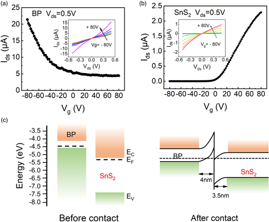
Fig. 2. (Color online) Electrical characteristics of individual BP and SnS2 FETs and energy band diagrams before and after contact. The transfer characteristics of (a) BP and (b) SnS2 FETs at Vds = 0.5 V. The insets are the output curves at different gate voltages by steps of 20 V in the range of −80 to 80 V. (c) Energy band alignment of BP/SnS2 heterostructure before and after contact.
Download figure:
Standard image High-resolution imageTo examine the carrier transport through the BP/SnS2 vdWHs under different bottom gate biases, a  of up to 0.5 V was applied to the electrode on the BP side, and the electrode on SnS2 was grounded. As shown in Fig. 3(a), the forward current rapidly increases to several tens of nA, while the reverse current reach to order of pA, showing clear rectification characteristics. We further studied the forward current transmission to investigate the rectification behavior and found two unique transmission mechanisms that can explain the transmission characteristics of our device, i.e. DT or Fowler–Nordheim tunneling (FNT),
9) as shown in the I–V curve replotted in Fig. 3(c). The I–V curve can be modeled based on a tunneling barrier with the Simmons approximation,
20,34) where DT occurs at low voltage and FNT dominates at higher voltage. The DT and FNT can be expressed by the following relation:
of up to 0.5 V was applied to the electrode on the BP side, and the electrode on SnS2 was grounded. As shown in Fig. 3(a), the forward current rapidly increases to several tens of nA, while the reverse current reach to order of pA, showing clear rectification characteristics. We further studied the forward current transmission to investigate the rectification behavior and found two unique transmission mechanisms that can explain the transmission characteristics of our device, i.e. DT or Fowler–Nordheim tunneling (FNT),
9) as shown in the I–V curve replotted in Fig. 3(c). The I–V curve can be modeled based on a tunneling barrier with the Simmons approximation,
20,34) where DT occurs at low voltage and FNT dominates at higher voltage. The DT and FNT can be expressed by the following relation:


where  is the barrier height, d is the tunneling barrier width, h is the Plank constant and
  is the effective mass of an electron. From the above Eqs. (1) and (2), we draw the Fowler–Nordheim plot, i.e.
  and
and  plot, as shown in Fig. 2(c). This plot clearly shows the transition from a logarithmic regime at small
  for DT to a linear regime with a negative slope at high
  for FNT, representing region I (blue) and region II (orange), respectively. The threshold voltage of FNT
  =1/8 = 0.125 V corresponds to
  indicating that the tunneling barrier is about 0.125 eV. According to the electrical characteristics, the band diagrams of reverse bias, small forward bias and forward bias when the gate voltage is zero are respectively shown as Fig. 4(d). Under reverse bias, due to the depletion of holes in BP and the accumulation of electrons in SnS2, the extremely low measured current results in almost no charge flowing through the heterostructure. At small forward bias (
 < 0.125 V), the high trapezoidal tunneling barrier at the interface dominates the charge transfer of DT. While, under a larger forward bias voltage (
 > 0.125 V), a lower triangular tunneling barrier at the interface appears with FNT. Moreover, we investigated the impacts of SnS2 channel length on the electrical characteristics of BP/SnS2 heterostructures. As shown in the Fig. 3(b), the device composed of 12 μm SnS2 channel shows a normal forward diode characteristic, that is, current in forward
  is much larger than that in reverse
  When the SnS2 channel decreases to 4 μm, the forward current has a significant increase compared to the case of 12 μm SnS2 channel. Simultaneously, the reverse current keeps constant at a small
  and then increases dramatically at a critical reverse voltage of about −0.15 V, which matches the performance of Zener diode.
35) Here, the case with 8 μm SnS2 channel is considered to be a middle state transformed from forward diode to Zener diode. In our case, the negative differential resistance phenomenon was obscured for two reasons: one is that the diffusion current and drift current are enhanced by the thermal energy at the room temperature;
36) the other is that the junction region needs to be composed of heavily doped p-type regions and heavily doped n-type regions.
15)
and then increases dramatically at a critical reverse voltage of about −0.15 V, which matches the performance of Zener diode.
35) Here, the case with 8 μm SnS2 channel is considered to be a middle state transformed from forward diode to Zener diode. In our case, the negative differential resistance phenomenon was obscured for two reasons: one is that the diffusion current and drift current are enhanced by the thermal energy at the room temperature;
36) the other is that the junction region needs to be composed of heavily doped p-type regions and heavily doped n-type regions.
15)
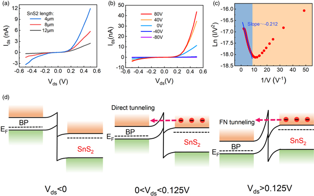
Fig. 3. (Color online) Diode behavior of the BP/SnS2 vdWHs. (a) Output characteristics at different  (b)
(b)  versus Vds at different SnS2 channel lengths. (c) Fowler–Nordheim plots. (d) Band diagrams of the junction under the different source-drain voltages.
Download figure:
Standard image High-resolution image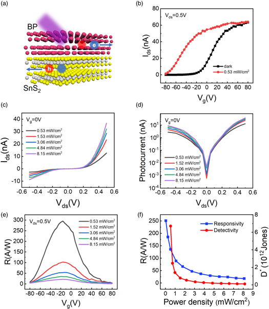
Fig. 4. (Color online) Photocurrent characteristics of the BP/SnS2 vdWHs. (a) Schematic of electron–hole pair generation with light illumination and charge carriers tunneling through the junction. (b) Ids–Vds curves under dark and 365 nm light illumination. (c) I–V curves under illumination with various incident power densities. (d) The log plots of these I–V curves. (e) The photoresponsivity of the heterostructure as a function of gate voltage under illumination with various power densities. (f) The photodetectivity ( ) and photoresponsivity (
 ) of the junction under illumination with various incident power densities, at Vds= 0.5 V.
Download figure:
Standard image High-resolution image
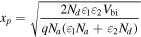
The widths of the depletion layers at the BP and SnS2 sides can be estimated by using the depletion model implemented on the conventional p–n heterostructures 34)
and
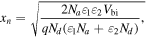
where  = 7.7 × 1017 cm−3,
  = 5.9 × 1017 cm−3, calculated by
  = n(p)/
 from hole and electron doping concentrations and thicknesses of BP and SnS2 with
  7.7 × 10¹¹ (1.54 × 10¹²) cm−2,
  13(20) nm.
  = 17.7 and
  = 7 are the dielectric constants of SnS2 and BP,
17,37) respectively, and the
= 7 are the dielectric constants of SnS2 and BP,
17,37) respectively, and the  0.125 V is the built-in potential at the junction extracted from the FNT curve above. Consequently,
 was calculated to be ≈ 4 (3.5) nm,as shown in Fig. 2(c).
Considering that the energy band structure is different from the familiar type-II p–n diodes, we have carried out photoresponsivity measurements to further explore the optoelectrical performance. Figure 4(a) illustrates the BP/SnS2 based vdWHs photodetector. The monochromatic light emitted by the laser sheds on the photodetector, generating a large number of electron–hole pairs in both the SnS2 and BP layers. These light-induced charge carriers tunnel is ultralow due to the depletion region between the BP/SnS2 heterostructure. When the device is under illumination, photon-excited carriers are generated in the 2D semiconductors, and these charge carriers can drift across the junction to generate photocurrent, resulting in a large  ratio of up to 2 × 10³ at a reverse bias of −64 V as shown in Fig. 4(b).
Figure 4(c) demonstrates the  at
at  = 0 V under optical irradiation (=365 nm) with various incident light powers. The photocurrent
  is defined as
  where
where  and
and  are the
  with and without light illumination, respectively. In addition, the differences in the I−V curves were also visualized by plotting the current versus voltage (
 versus
  ) on a logarithmic scale [Fig. 4(d)]. When
  is negative value, the current shows a significant increase under light, indicating that the junction has a strong light response. Figure 4(e) plots the relationship between the light responsivity (
 ) and
) and  of the heterostructure under different illumination intensities, where
  is the illumination power,
  is the effect response area and
  is the photocurrent. Moreover, the data of
  is obtained from Fig. 4(c), and the high photoresponsive performance can be obtained at
  = −16 V (295.3 A W−1). Another important parameter of photodetector is photodetectivity, which is described by the following equation
  showing the ability to detect weak light signals. Figure 4(f) shows the photoresponsivity
  and photodetectivity
  as a function of
  at
at  = 0.5 V. It is worth noting that type-III band-aligned photodiode structure has a larger bandgap, which will produce a high potential barrier, thereby suppressing the generation of dark current and the photodetectivity can be estimated to be
  6.72 × 10¹² Jones under a light intensity of 0.53 mW cm−2, which is 10–1000 times higher than that of other SnS2-based photodetector.
10,38,39)
6.72 × 10¹² Jones under a light intensity of 0.53 mW cm−2, which is 10–1000 times higher than that of other SnS2-based photodetector.
10,38,39)
4. Conclusion
In conclusion, we have demonstrated a highly sensitive photodetector using vdWHs with broken-gap energy band alignment composed of BP and SnS2. The BP/SnS2 vdWHs shows strong interlayer charge coupling verified by Raman. Multifunctional diode is achieved by changing the channel length of SnS2, which results from the increase of effective drain bias voltage. Furthermore,the BP/SnS2 vdWHs exhibits ultrahigh photodetectivity of 6.72 × 10¹² Jones ( ratio of
  2 × 10³) and high photoresponsivity of 295.3 A W−1. The dark-carrier tunneling was highly suppressed by the depletion region of the junction whereas the photocarrier tunneling was efficiently improved by the high DT current when illuminated,which has been confirmed by the energy band structures and electrical characteristics fitted with DT.
Acknowledgments
This work was supported by the National Key R&D program of China (Grant No. 2019YFB2005600), the National Natural Science Foundation of China (Grant No. 51732010, 51802341), the China Postdoctoral Science Foundation (Grant No. 2020M671592).