
Abstract
The effect of Si surface atomically flattening (SAF) on the Hf-based metal/oxide/nitride/oxide/Si (MONOS) nonvolatile memory (NVM) characteristics was investigated. The memory window (MW) obtained in the C–Vcharacteristics for the Hf-based MONOS diode was increased from 4.5 to 4.8 V by the Si SAF. The charge centroid (Zeff) was found to be shifted from the center of the HfN1.1 charge trapping layer (CTL) to the interface at block layer and CTL for the Hf-based MONOS diode with the Si SAF. Furthermore, the MW of 3.2 V was realized for the Hf-based MONOS NVM with improvement of device characteristics by Si SAF.
Export citation and abstract BibTeX RIS

Content from this work may be used under the terms of the Creative Commons Attribution 4.0 license. Any further distribution of this work must maintain attribution to the author(s) and the title of the work, journal citation and DOI.
1. Introduction
Metal–oxide–nitride–oxide–silicon (MONOS) type nonvolatile memory (NVM) is a promising candidate to replace the conventional floating-gate type NVM in terms of the scaling and high-density integration.1) One of the issues of conventional MONOS type NVM is the high operation voltage such as 20 V because the thinning of ONO layers has been limited for the ONO layers which consist from SiO2 blocking layer (BL)/SiN charge trapping layer (CTL)/SiO2 tunneling layer (TL). Therefore, the replacement of each layer to high-k thin film has been investigated to decrease the equivalent oxide thickness of ONO layers for the operation voltage reduction especially for the BL and CTL.2–6) Generally, each layer is deposited by a different method such as thermal oxidation for SiO2 TL, chemical vapor deposition for SiN CTL, and sputtering for high-k BL. This process would degrade the interface properties during the transfer of the sample to another chamber.
The HfO2 thin film with the relative dielectric constant (εr) of 20 has been introduced to the metal–oxide-field-effect transistor (MOSFET) as a high-k gate insulator since the 45 nm technology node.7) The HfNx (x > 1) thin film has also been investigated for high-k gate insulator application, and the εr of 26 has been achieved for the HfN1.3/HfN1.1/Si(100) bilayer structures.8–11) We have reported the excellent electrical characteristics of fully in situ formed Hf-based MONOS NVM, which consists from HfN0.5 gate electrode/HfO2 BL/HfN1.1 CTL/HfO2 TL/Si(100).12–14) The Hf-based MONOS layers were deposited by the electron cyclotron resonance (ECR) plasma sputtering in a chamber with changing the process gas for the deposition of each layer. The relative dielectric constants of HfO2 and HfN are several times higher than those of SiO2 and SiN such as 3.9 and 7, respectively, which would realize the high speed and low voltage operation. The HfO2 TL is effective in improving the efficiency of electron injection and emission compared to the SiO2 TL because of its small barrier height to Si. However, the HfO2 TL becomes as thin as a few nanometers, further improvement of MONOS memory characteristics has been getting difficult.
In order to improve the Hf-based MONOS memory characteristics, Si surface flattening is important as well as the gate insulator of MOSFET15–23) because of the thinning of HfO2 TL and HfN1.1 CTL. We have reported the Si surface atomically flattening (SAF) process for the Si(100) surface by annealing in Ar/H2 ambient.24–32) It has been revealed that the electrical characteristics of Hf-based MONOS diodes was improved by Si SAF as well as the MOSFETs with Hf-based high-k gate insulator.28–32)
In this study, the effect of Si SAF on the Hf-based MONOS NVM was investigated.33) Furthermore, the charge centroid in the HfN1.1 CTL was extracted.33) The precise device analysis was carried out for the Hf-based MONOS NVM.
2. Experimental procedure
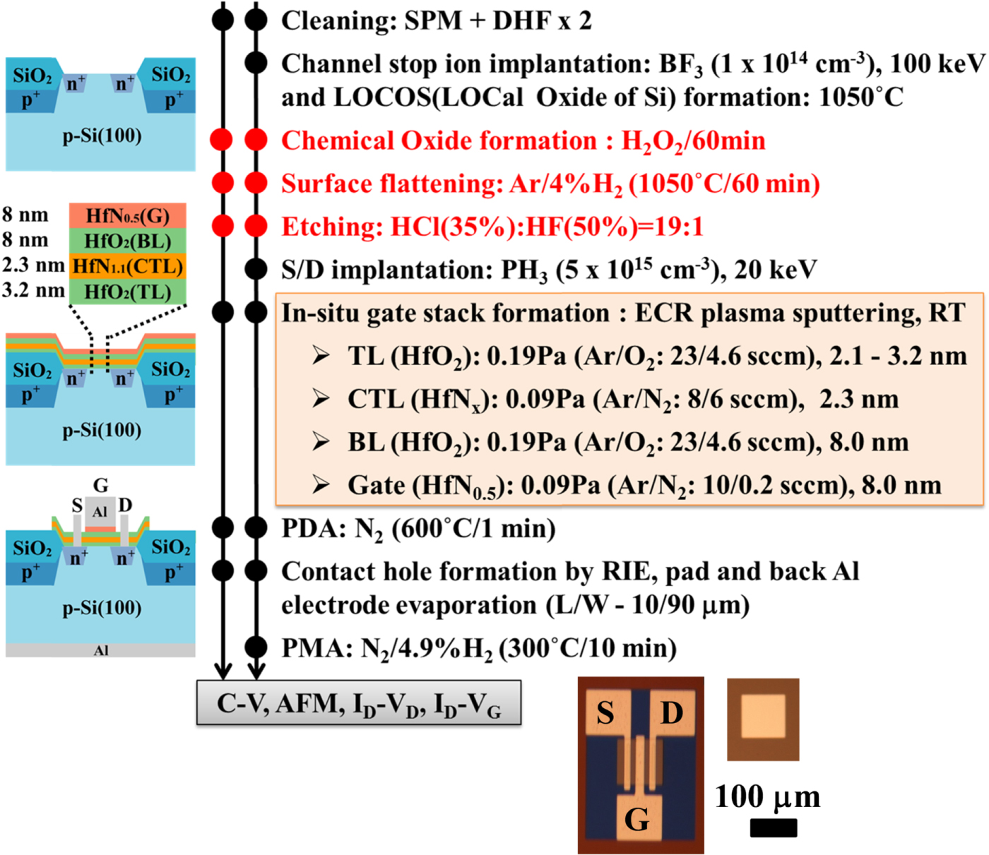
Figure 1 shows the experimental procedure for the fabrication of Hf-based MONOS NVM and diode. The in situ formed Hf-based MONOS NVM was fabricated on p-Si(100) substrate using the typical gate-last process.14) After the channel stop ion implantation and local oxidation of silicon (LOCOS) isolation, Si(100) SAF process by annealing at 1050 °C/60 min in Ar/4%H2 ambient was carried out. Then, the HfN0.5/HfO2/HfN1.1/HfO2 (MONO) structure was in situ deposited on p-Si(100) by the ECR plasma sputtering (AFTEX 3400) at room temperature (RT). The designed thickness of HfO2 TL was 3.2 nm. A 2.1 nm TL was also investigated for the comparison. The HfN1.1 CTL thickness was 2.3 nm. The thickness of HfO2 BL and HfN0.5 gate electrode was 8 nm each. The Ar/O2 flow rate for HfO2 TL and BL was 23/4.6 sccm, while the Ar/N2 flow rates for HfN1.1 CTL and HfN0.5 gate electrode were 8/6 sccm and 10/0.2 sccm, respectively. Then, the post-deposition annealing (PDA) was carried out at 600 °C/1 min in N2. After the contact hole formation and metallization, the post-metallization annealing (PMA) was carried out at 300 °C/10 min in N2/4.9%H2. The gate length (L) and width (W) of the fabricated device was L/W = 10/90 μm. The inset of Fig. 1 shows the plane-view of the fabricated Hf-based MONOS diode and NVM.

Fig. 1. (Color online) Fabrication process of Hf-based MONOS NVM with Si SAF.
Download figure:
Standard image High-resolution imageThe fabricated Hf-based MONOS diodes and NVMs were evaluated by C–V, density of interface states (Dit), ID–VD, and ID–VG at RT using LCR meter (HEWLETT PACKARD 4284A) and semiconductor parameter analyzer (Agilent 4156C). The operation conditions were set as the program voltage/time (VPGM/tPGM) of 10 V/1 s, the erase voltage/time (VERS/tERS) of −10 V/1 s, and VDS of 1.5 V. The charge centroid (Zeff) was extracted utilizing the following equation

where Qm is the measured charge, εox is the dielectric constant of HfO2 BL, and VFB is the flat-band voltage.34) Figure 2 shows the schematic measurement system for Zeff evaluation. The input pulse was applied by pulse generator (HEWLETT PACKARD 8110A), and the pulse was observed by the oscilloscope (LeCroy LC534AM). The charge was measured by the electrometer (KEITHLEY 6517A). The pulse input, charge and C–V measurements were controlled by the switch (KEYSIGHT DAQ970A). All measurements were carried out at RT.

Fig. 2. (Color online) Schematic Zeff evaluation system.
Download figure:
Standard image High-resolution image3. Results and discussion
3.1. Effect of Si SAF on the Hf-based MONOS diode characteristics
Figure 3 shows the effect of Si SAF on the C–V measured at 1 MHz and memory window (MW) for Hf-based MONOS diodes extracted from the difference of flat-band voltage (VFB) after the program and erase (P/E) operation at +10 V/1 s and −10 V/1 s, respectively. From Fig. 3(a), it was found that the charge-injection type hysteresis width was decreased from 40 to 10 mV by the Si SAF for the Hf-based MONOS diodes with the 3.2 nm thick HfO2 TL. This improvement of interface property was also confirmed by the reduction of Dit from 5.7 × 10¹⁰ to 3.5 × 1010 cm−2 eV−1 by the Si SAF as we have reported.13) The ideal VFB for HfN0.5 gate electrode and p-Si(100) was −0.2 V so that the VFB shit was decreased from −1.1 to −0.9 V by the Si SAF. This is probably due to the reduction of fixed-oxide charge in the HfO2 TL with improving the film quality by the Si SAF. The positive fixed charge is induced by the SiOx (x < 2.0) formation at the interface of HfO2 and Si substrate. The rough Si surface would form the thicker SiOx layer, and it would be suppressed by the Si SAF. Figure 3(b) shows the effect of Si SAF on the MW for the Hf-based MONOS diode as a function of the thickness of HfO2 TL. As shown in Fig. 3(b), the MW obtained by the P/E operation was increased from 4.5 to 4.8 V by the Si SAF when the HfO2 TL thickness was 3.2 nm. It was getting more effective for the thinner HfO2 TL such as 2.1 nm. The MW was increased from 1.5 to 2.5 V in case of the Hf-based MONOS diodes with 2.1 nm thick HfO2 TL. This is because the interface roughness induced the degradation of the retention for the trapped charge with decreasing the HfO2 TL thickness.

Fig. 3. (Color online) The effect of Si SAF on (a) C–V (1 MHz) and (b) MW of Hf-based MONOS diodes.
Download figure:
Standard image High-resolution imageFigure 4 shows the extracted Zeff for the Hf-based MONOS diodes with 2.3 nm thick HfN1.1 CTL and 3.2 nm HfO2 TL utilizing Eq. (1).34) The εr of HfO2, εHfO2, was assumed as 20. The distance of Zeff from HfO2 BL/HfN1.1 CTL interface was extracted as 1.3 nm, which is approximately at the center of HfN1.1 CTL, for the Hf-based MONOS diode without Si SAF. Interestingly, it was found that the Zeff was located at the interface region of HfO2 BL/HfN1.1 CTL for the Hf-based MONOS diode with Si SAF. The Si SAF would improve the uniformity of HfO2 TL and HfN1.1 CTL which led to improve the stability of trapped charge in the HfN1.1 CTL and decrease the probability of detrapping of the electrons in the HfN1.1 CTL through the HfO2 TL.

Fig. 4. (Color online) The effect of Si SAF on Zeff.
Download figure:
Standard image High-resolution image3.2. Improvement of Hf-based MONOS NVM characteristics by Si SAF
Next, we have investigated the effect of Si SAF on the device characteristics of Hf-based MONOS NVM with 2.3 nm thick HfN1.1 CTL and 3.2 nm HfO2 TL. Figure 5 shows the ID–VD characteristics for the fabricated Hf-based MONOS NVM at fresh state. The threshold voltage (VTH) was extracted from the ID–VG characteristics as shown in Fig. 6, and the MW was defined as the VTH difference of program and erase states. As shown in Fig. 5, the good saturation characteristics were observed for the ID–VD characteristics under the VG–VTH of 2 V operation for Hf-based MONOS NVM both with and without (w/o) Si SAF. This result suggested that the device fabrication process was successfully carried out especially for the S/D contact hole formation and gate patterning for the Hf-based MONOS stacked structures. The current drivability was found to be improved by Si SAF with the linear mobility of 150 cm2 V−1 s−1.

Fig. 5. (Color online) The effect of Si SAF on ID–VD. The L/W was 10/90 μm.
Download figure:
Standard image High-resolution image
Fig. 6. (Color online) ID–VG of Hf-based MONOS NVM (a) without and (b) with Si SAF. The L/W was 10/90 μm. The ON/OFF ratio was extracted from the fresh characteristics.
Download figure:
Standard image High-resolution image
Figure 6 shows the effect of Si SAF on the ID–VG characteristics of Hf-based MONOS NVM utilizing P/E pulses of ±10 V/1 s. The read operation condition was set as VD = 1.5 V and VS = 0 V, respectively. The VTH was defined as the voltage when the ID became 10−2 A μm−1 in this research. The extracted VTH results were indicated by an arrow in each graph. The obtained ID–VG characteristics showed negligible hysteresis both for the devices with and w/o Si SAF. As shown in Fig. 6(a), the initial VTH was −0.9 V, while it shifted to 1.7 V after the program operation. The VTH of 0.6 V was obtained after the erase operation. Although the erase operation was not completed by this condition, the MW of 1.1 V was obtained for the Hf-based MONOS NVM w/o Si SAF.
The device characteristics were markedly improved by the Si SAF as shown in Fig. 6(b). The initial VTH was −0.4 V, while it shifted to 3.3 V after the program operation. Interestingly, the erase operation was significantly improved by the Si SAF, and the VTH shifted to 0.1 V which was close to the initial state. The MW of 3.2 V was obtained for the Hf-based MONOS NVM with Si SAF. Furthermore, the extracted ON/OFF ratio form the fresh characteristics was increased from 6.5 × 10⁷ to 2.9 × 10⁸, and subthreshold swing was reduced from 106 to 101 mV dec−1 with decreasing the off current by the Si SAF. The Si SAF improves the uniformity of HfO2 TL and HfN1.1 CTL which led to the decrease of off leakage current. Furthermore, we speculated that the deep trap level was formed in the HfN1.1 CTL in case of the Hf-based MONOS NVM w/o Si SAF which caused the incomplete erase operation. The deep trap formation would be suppressed by the Si SAF with improving the film quality of HfN1.1 CTL so that the erase operation was successfully carried out. Therefore, the Si SAF improved not only the quality of each layer but the property of each interface, and it is promising for precise control of the VTH to realize the multi-bit NVM with reducing the operation voltage. We have reported that the improvement of memory characteristics such as retention and endurance by the Si SAF for the Hf-based MONOS diodes.13) The retention and endurance characteristics for the Hf-based MONOS transistors would be discussed in another paper.
4. Conclusions
The effect of Si SAF on the Hf-based MONOS characteristics was investigated. The MW of 4.8 V was obtained, and Zeff was found to be located at BL/CTL interface for the Hf-based MONOS diode with the Si SAF. Furthermore, the MW of 3.2 V was realized for the Hf-based MONOS NVM with improvement of the device characteristics by the Si SAF. In conclusion, the Si SAF is effective to improve the Hf-based MONOS NVM characteristics for high speed and low voltage operation.
Acknowledgments
The authors would like to thank Mr. M. Suzuki of Tokyo Institute of Technology, the late Prof. Emeritus T. Ohmi, Prof. T. Goto, and Prof. T. Suwa of Tohoku University, Dr. M. Shimada and Mr. M. Hirohara of JSW-AFTY for their support and useful discussions for this research. This research was partially supported by JSPS KAKENHI Grant Nos. 19H00758, JP17J10752 and Toshiba Electronic Devices & Storage Corporation.