
Abstract
Partial dislocation (PD) combinations near the substrate/epilayer interface and the epilayer surface of 4H-SiC are analyzed for bar-shaped single Shockley-type stacking faults (1SSFs) by plan-view transmission electron microscopy (TEM) with the aid of photoluminescence imaging. Although the PDs are found to have a zigzag structure similar to that found in triangular 1SSF by TEM observation, the combination is thought to be different, consisting of a 30° Si-core + 90° Si-core for the triangular 1SSF and 30° Si-core + 30° C-core for the bar-shaped 1SSF. The features of the basal plane dislocation at the origin are speculated by also identifying the converted threading edge dislocation by additional Burgers vector determination of the PD loop by TEM.
Export citation and abstract BibTeX RIS
1. Introduction
Problems such as forward voltage degradation and reduced blocking voltage, which are observed mainly in bipolar devices and even in metal–oxide–semiconductor field-effect transistors and junction barrier Schottky or merged PiN Schottky diodes fabricated on 4H-silicon carbide (SiC) with a p–n junction in the structure, are widely known to be attributable to the expansion of single Shockley-type stacking faults (1SSFs) in the epitaxial layer that originates from basal plane dislocations (BPDs). 1–9) The expansion of these 1SSF domains is explained by migration of Si-core [Si(g)] 30° Shockley partial dislocations (PDs) 10) under forward biasing, where electron–hole recombination enhances the dislocation glide. 11,12) This is thought to be one of the remaining serious issues preventing the development of power devices with 100% reliability. Therefore, there is strong demand for the establishment of screening methods. Although the structure of BPDs has been reported to be pairs of PDs on the basal plane with 1SSFs between them, 1,13–15) differences in the combinations of PDs cause the 1SSF shapes to differ as they expand, resulting in triangular 1SSFs, 4) trapezoidal 1SSFs, 4) bar-shaped 1SSFs (with or without a triangle), 7) and double-rhombic 1SSFs. 16) The threshold current density for expansion and the expansion rate have also been reported to be dependent on the 1SSF shape. 17,18) However, the mechanisms that determine the expansion rate for each 1SSF shape are not fully understood.
Since we believe that structural elucidation is essential for understanding and controlling this issue, we have previously investigated the detailed structure of triangular 1SSFs in which the right-angle is at the shallower side in the epilayer using photoluminescence (PL) and transmission electron microscope (TEM) analysis.
18–22) In addition, a triangular 1SSF with the right-angle at the deeper side in the epilayer was also examined,
23,24) with the BPD at the origin found to have converted from a threading edge dislocation (TED) at a relatively shallow region of the epilayer (1.6 μm deep from the surface) with the converted BPD then changing direction toward the surface at around 1.5 μm deep.
23) This configuration from a deep TED to a shallow TED via a BPD is referred to as "TED-BPD-TED." A similar structure to the BPD at the origin was found to expand into an inclined double-rhombic 1SSF.
25) The difference in expansion shapes of the 1SSFs was explained by the different characters of the BPDs at the origin, such as a perfect screw dislocation with Burgers vector (
b
BPD) = (1/3)[11 0] to a triangular 1SSF and a 60° perfect dislocation with
b
BPD = (1/3)[
0] to a triangular 1SSF and a 60° perfect dislocation with
b
BPD = (1/3)[ 110] or (1/3)[1
 10] to an inclined double-rhombic 1SSF.
26) The threshold current density for expansion and the expansion rate have also been reported to be dependent of the 1SSF shapes.
17,27) From the viewpoint of the electrical properties of power devices, a correlation between 1SSFs and blocking voltage degradation has been reported.
28) We think that structural elucidation is essential for understanding and controlling the issue.
10] to an inclined double-rhombic 1SSF.
26) The threshold current density for expansion and the expansion rate have also been reported to be dependent of the 1SSF shapes.
17,27) From the viewpoint of the electrical properties of power devices, a correlation between 1SSFs and blocking voltage degradation has been reported.
28) We think that structural elucidation is essential for understanding and controlling the issue.
It has been noted that the terminating boundaries of 1SSFs are straight lines along the [ 100] direction as observed by electroluminescence (EL) and PL imaging regardless of the expanding shape. Termination near the substrate/epilayer interface is explained by a lack of driving force because the usual substrate has a much higher donor concentration and lower minority carrier lifetime, such that the excess carrier concentration
29,30) no longer satisfies the recombination enhanced dislocation glide.
11,12) However, termination near the surface side is explained by insufficient electron density in the p-type anode region. We have previously investigated the detailed structure of triangular 1SSFs, particularly in the vicinity of terminated areas on the shallower side and the deeper side of the epilayers, and TEM analysis revealed zigzag configurations consisting of combinations of 30° Si(g) and 90° Si(g) PDs, which were previously thought to be straight lines in both areas.
19,24)
100] direction as observed by electroluminescence (EL) and PL imaging regardless of the expanding shape. Termination near the substrate/epilayer interface is explained by a lack of driving force because the usual substrate has a much higher donor concentration and lower minority carrier lifetime, such that the excess carrier concentration
29,30) no longer satisfies the recombination enhanced dislocation glide.
11,12) However, termination near the surface side is explained by insufficient electron density in the p-type anode region. We have previously investigated the detailed structure of triangular 1SSFs, particularly in the vicinity of terminated areas on the shallower side and the deeper side of the epilayers, and TEM analysis revealed zigzag configurations consisting of combinations of 30° Si(g) and 90° Si(g) PDs, which were previously thought to be straight lines in both areas.
19,24)
In the present paper, we focus on the structure of the PDs both near the substrate/epilayer interface and near the epilayer surface side where the bar-shaped 1SSFs terminate. A structural comparison is attempted between bar-shaped and triangular 1SSFs. 31) In addition, the structure of the BPD at the origin was estimated and the 1SSF expanding model proposed for the triangular 1SSF cases 24) is extended to cover the bar-shaped 1SSF cases.
2. Experimental methods
To obtain EL images of 1SSF expansion under forward current injection, PiN diodes were fabricated on a commercially available n-type 4H-SiC epitaxial wafer with a 4° off-cut toward the [11 ] direction. The diodes consisted of a 9.4 μm thick n-type drift layer (3 × 1015 cm−3) with a 0.6 μm thick p-type anode layer (about 3 × 1020 cm−3) at the top. The p-type region was formed by aluminum ion implantation. Line-and-space-shaped open window metal contacts were used for the anode electrode. The diode structure employed in this study is schematically shown in Fig. 1(a). An EL image of a diode chip after a high-current stress test at 700 A cm−2 for 10 min, in which triangular 1SSFs have expanded from near the substrate/epilayer interface toward the surface, is shown in Fig. 1(b). After removing the electrode metal and passivation film chemically, PL imaging was performed using a 420 nm (full width at half maximum, 10 nm) bandpass filter (BPF) with the excitation by Hg–Xe lamps with a 313 nm BPF (1.53 W cm−2), as shown in Fig. 1(c), indicating a bar-shaped 1SSF (bright contrast
32)) on the chip that was not observed during the preceding EL observation owing to the bonding wire. Molten KOH etching was carried out to reveal dislocation etch pits for several minutes at 500 °C. Figure 1(d) shows a magnified PL image, which was acquired using a 600 nm BPF to observe the bright contrast of the 1SSF termination near the epilayer surface.
19) PD contrast and etch pits were observed clearly enough to give certainty to the focused ion beam (FIB) sampling areas as also shown in Fig. 1(d) by a square and a rectangle in the substrate/epilayer and surface side, respectively, for the following plan-view TEM observation.
] direction. The diodes consisted of a 9.4 μm thick n-type drift layer (3 × 1015 cm−3) with a 0.6 μm thick p-type anode layer (about 3 × 1020 cm−3) at the top. The p-type region was formed by aluminum ion implantation. Line-and-space-shaped open window metal contacts were used for the anode electrode. The diode structure employed in this study is schematically shown in Fig. 1(a). An EL image of a diode chip after a high-current stress test at 700 A cm−2 for 10 min, in which triangular 1SSFs have expanded from near the substrate/epilayer interface toward the surface, is shown in Fig. 1(b). After removing the electrode metal and passivation film chemically, PL imaging was performed using a 420 nm (full width at half maximum, 10 nm) bandpass filter (BPF) with the excitation by Hg–Xe lamps with a 313 nm BPF (1.53 W cm−2), as shown in Fig. 1(c), indicating a bar-shaped 1SSF (bright contrast
32)) on the chip that was not observed during the preceding EL observation owing to the bonding wire. Molten KOH etching was carried out to reveal dislocation etch pits for several minutes at 500 °C. Figure 1(d) shows a magnified PL image, which was acquired using a 600 nm BPF to observe the bright contrast of the 1SSF termination near the epilayer surface.
19) PD contrast and etch pits were observed clearly enough to give certainty to the focused ion beam (FIB) sampling areas as also shown in Fig. 1(d) by a square and a rectangle in the substrate/epilayer and surface side, respectively, for the following plan-view TEM observation.

Fig. 1. (Color online) PiN diode chip used for the analysis: (a) schematic cross-sectional structure of the PiN diode, (b) EL image, (c) PL image (420 nm BPF), and (d) magnified PL image after KOH etching to show the TEM sampling positions observed with a 600 nm BPF.
Download figure:
Standard image High-resolution imageIn the plan-view TEM observation in both positions, the Burgers vector
b
was estimated under the two-beam conditions by
g
·
b
contrast analysis by changing the diffraction vectors
g
of 11 0, 1
0, 1 10, and
  110 on the FIB sampled specimens at an acceleration voltage of 300 kV.
3. Results and discussion
3.1. Surface side
Figure 2 shows the bright-field plan-view TEM images at the surface side of the 1SSF termination. Figure 2(a) shows an image acquired using a slight inclination to enhance the 1SSF contrast after the zone-axis condition was satisfied. The dislocation contrast disappears when
g = 11 0, as shown in Fig. 2(b), which suggests that Burgers vector for this PD loop (
b
PD) is ±(1/3)[1
0, as shown in Fig. 2(b), which suggests that Burgers vector for this PD loop (
b
PD) is ±(1/3)[1 00]. As seen in Fig. 2, the dislocation contrast is also found to disappear in the [1
 00] direction (lower side) under any conditions. This feature indicates that the dislocation has already been etched off. Figure 3(b) shows an enlarged scanning electron microscope (SEM) image acquired on the surface side of the 1SSF termination before the plan-view TEM sampling by FIB. The observation area is indicated by orange dashed lines to show the position on the PL image in Fig. 3(a). Aligned zigzag pits can be observed in the SEM image in Fig. 3(b), indicating that the remaining PD lines are along the Peierls valley, namely, the ±[
 ] and ±[
 ] directions. The zigzag structure of the KOH etch pits was observed on the terminating line of the triangular 1SSF that corresponds to 30° Si(g) and 90° Si(g) PDs,
33) where the direction of the etch pits formed on the 90° Si(g) PDs was not symmetric with the 30° Si(g) PDs. However, the zigzag shape observed in Fig. 3 had a higher vertical symmetry. This implies that the terminating line has two 30° PDs with
b
PD = ±(1/3)[1
] directions. The zigzag structure of the KOH etch pits was observed on the terminating line of the triangular 1SSF that corresponds to 30° Si(g) and 90° Si(g) PDs,
33) where the direction of the etch pits formed on the 90° Si(g) PDs was not symmetric with the 30° Si(g) PDs. However, the zigzag shape observed in Fig. 3 had a higher vertical symmetry. This implies that the terminating line has two 30° PDs with
b
PD = ±(1/3)[1 ].
].
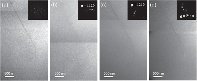
Fig. 2. Bright-field TEM images at the surface side: (a) slightly inclined from zone-axis condition, (b) two-beam condition with
g
= 11 0, (c) two-beam condition with
g = 1
0, (c) two-beam condition with
g = 1 10, and (d) two-beam condition with
g =
10, and (d) two-beam condition with
g =  110.
110.
Download figure:
Standard image High-resolution image
Fig. 3. (Color online) Images of the surface side: (a) PL image (600 nm BPF) showing the plan-view TEM sampling position and SEM observation position and (b) an enlarged SEM image.
Download figure:
Standard image High-resolution imageFigure 4 shows the estimated structure of the BPD at the origin, according to the dislocation loop model.
34,35) The classification according to Ref. 36 was determined to be (a35), which means the directions of
b
BPD and ξ were both ±[1 10], and the BPD was thus a perfect screw dislocation in this case and the glide-type of the BPD is type B.
34–36) The type of glide was categorized by the layer that contains the rotational glide: type A for the BPD loop on either layer with tetrahedrons facing the [
10], and the BPD was thus a perfect screw dislocation in this case and the glide-type of the BPD is type B.
34–36) The type of glide was categorized by the layer that contains the rotational glide: type A for the BPD loop on either layer with tetrahedrons facing the [ ] direction, and type B for the BPD loop on either layer with tetrahedrons facing the [1
 ] direction, when looking at (11
 ).
34,35) If the BPD had been a 60° perfect dislocation, it would have expanded as a double-rhombic 1SSF.
26) The BPD at the origin might have converted into a TED in the epilayer. Note that care is required because the expanding shapes of 1SSFs differ depending on the places where the BPDs at the origin were located, namely, near the substrate/epilayer side or the surface side, even for the same combination of
b
BPD and the line direction, ξ. In the current case, the conversion point from the BPD at the origin to the TED is expected to be located near the substrate/epilayer side. This estimation is derived by the bottom-slanted line direction of the 1SSF, as shown in Fig. 1(c). If the conversion point was near the surface, as shown at the lower TED-BPD case in Fig. 4, the expansion shape of 1SSF would be different. According to the PD combination shown in Fig. 4, the terminating PDs on the surface side turn out to be a 30° Si(g) with ξ = ±[
).
34,35) If the BPD had been a 60° perfect dislocation, it would have expanded as a double-rhombic 1SSF.
26) The BPD at the origin might have converted into a TED in the epilayer. Note that care is required because the expanding shapes of 1SSFs differ depending on the places where the BPDs at the origin were located, namely, near the substrate/epilayer side or the surface side, even for the same combination of
b
BPD and the line direction, ξ. In the current case, the conversion point from the BPD at the origin to the TED is expected to be located near the substrate/epilayer side. This estimation is derived by the bottom-slanted line direction of the 1SSF, as shown in Fig. 1(c). If the conversion point was near the surface, as shown at the lower TED-BPD case in Fig. 4, the expansion shape of 1SSF would be different. According to the PD combination shown in Fig. 4, the terminating PDs on the surface side turn out to be a 30° Si(g) with ξ = ±[ ] and a 30° C-core [C(g)] with ξ = ±[
![$\bar{1}0]$](https://content.cld.iop.org/journals/1347-4065/62/SC/SC1001/revision2/jjapaca033ieqn25.gif) .
.
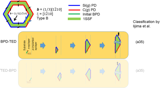
Fig. 4. (Color online) Structural estimation of the BPD at the origin and PDs at both terminating sides.
Download figure:
Standard image High-resolution image3.2. Substrate/epilayer side
A plan-view TEM sample on the substrate/epilayer side was taken by FIB as shown in Fig. 1(d). From the horizontal distance, L = 131 μm, measured on the PL image in Fig. 1(d), the center depth, d, of the TEM sample was calculated from d = L/tan(4°), that is, 9.2 μm. Figure 5(a) shows the bright-field plan-view TEM images. During the TEM observation, deeper PDs were found to move toward the shallower side, corresponding to 1SSF shrinkage. Before the TEM observation, the bar-shaped 1SSF had almost parallel boundary lines at the surface side and the substrate/epilayer interface side as seen in Fig. 1(c) or Fig. 3(a). After the TEM observation, the upper portion of the 1SSF became thinner by inclining the line close to substrate/epilayer interface as shown in Figs. 5(a), 5(b), 6, and 8 (which will appear later). It was determined from Fig. 4 that both terminating lines consist of 30° Si(g) and 30° C(g) PDs. Figure 5(b) shows a schematic shape of the dislocation contrast in Fig. 5(a). The blue and red lines correspond to the Si(g) and C(g) PDs, respectively. The core species were derived from the dislocation loop model
34) shown in Fig. 4 or 5(c). The dislocation lines are thought to be constructed from the PDs shown as bold purple double-ended arrows in Fig. 5(c), where
b
PD was determined to be ±(1/3)[1  ] from additional
g
·
b
contrast analysis using the two-beam condition in TEM, where the dislocation contrast disappeared when
g = 11
] from additional
g
·
b
contrast analysis using the two-beam condition in TEM, where the dislocation contrast disappeared when
g = 11 . These results show that the same features but having symmetrical ξ were identified at the substrate/epilayer side of the 1SSF termination, namely, 30° Si(g) with ξ = ±[
 ] and 30° C(g) PDs with ξ = ±[
 ].
].

Fig. 5. (Color online) Plan-view TEM observation at the substrate/epilayer side: (a) bright-field TEM images, (b) schematic illustration of the partials, and (c) dislocation loop model.
Download figure:
Standard image High-resolution image3.3. BPD-TED conversion point
Next, we attempted to obtain experimental evidence of the BPD-TED conversion on the deeper side. Figure 6(a) shows the PL image (420 nm BPF) acquired after plan-view TEM observations in Sects. 3.1 and 3.2. In Fig. 6(a), the dark roundish contrast corresponds to the etch pits. The etch pits can be classified by size. The smallest ones are considered to be TED-related.
37) There are two candidates of TED etch pits observed in Fig. 6(a), where the conversion might have occurred, named TED1 and TED2. There are two possible cases as schematically shown in Fig. 6(b). In case 1, TED1 was converted from the BPD near the substrate/epilayer interface, while in case 2, TED2 was from the BPD penetrated to the epilayer and close to the surface. The etch pit around TED2 was chosen for observation by SEM and another plan-view TEM sampling area was decided, because it seemed closer to the PD loop. Figure 7(a) shows the SEM image in which the TED2 pit has two accompanying small pits, named PD1 and PD2. Another small PD pit was observed and is thought to have penetrated to the surface of the epilayer. Figure 7(b) shows the TEM image with low magnification. The FIB sampled thin film for the TEM observation had a borehole where there was an etch pit owing to TED2. Figures 7(c) and 7(d) show the results of
g
·
b
contrast analysis at PD2 and PD1, respectively. In both PDs, the dislocation contrast disappeared when
g = 11 . These results indicate that both PDs are
b
PD = ±(1/3)[1
. These results indicate that both PDs are
b
PD = ±(1/3)[1 ]. This narrows down the alternative cases shown in Fig. 6(b) to Case 1, in which TED2 is not involved in the conversion or the
b
PD changing point of the PD loop of the boundary of the bar-shaped 1SSF. In Fig. 6(a), the TED1 pit seems away from the PD loop. However, TEDs are not always parallel to the 〈0001〉 direction and inclined by several degrees.
38,39) Therefore, it is a possible distance when the TED1 etch pit is observed from the 4° off-cut (0001) surface and the conversion point is located about 10 μm deep from the surface.
40) As seen in Fig. 6(a), the size of the etch pits around TED1 and TED2 appeared to be almost the same. If TED2 had been converted from a BPD, the conversion point would have been close to the epilayer surface, as in Case 2, and the size of the etch pit around TED2 would have likely been smaller as the length of TED2 would be very short compared with thickness of the entire epilayer. Thus, it is reasonable to conclude that TED1 was the converted threading dislocation from the deeper BPD (Case 1). The overall structure was confirmed as shown in Fig. 8. Therefore, the BPD at the origin, depicted by dashed green line in Fig. 8, should be type B with
b
BPD = ±(1/3)[1
]. This narrows down the alternative cases shown in Fig. 6(b) to Case 1, in which TED2 is not involved in the conversion or the
b
PD changing point of the PD loop of the boundary of the bar-shaped 1SSF. In Fig. 6(a), the TED1 pit seems away from the PD loop. However, TEDs are not always parallel to the 〈0001〉 direction and inclined by several degrees.
38,39) Therefore, it is a possible distance when the TED1 etch pit is observed from the 4° off-cut (0001) surface and the conversion point is located about 10 μm deep from the surface.
40) As seen in Fig. 6(a), the size of the etch pits around TED1 and TED2 appeared to be almost the same. If TED2 had been converted from a BPD, the conversion point would have been close to the epilayer surface, as in Case 2, and the size of the etch pit around TED2 would have likely been smaller as the length of TED2 would be very short compared with thickness of the entire epilayer. Thus, it is reasonable to conclude that TED1 was the converted threading dislocation from the deeper BPD (Case 1). The overall structure was confirmed as shown in Fig. 8. Therefore, the BPD at the origin, depicted by dashed green line in Fig. 8, should be type B with
b
BPD = ±(1/3)[1 ] and ξ = ±[1
 ] in which one of the Shockley PD was 30° Si(g) with
b
PD = ±(1/3)[1
] in which one of the Shockley PD was 30° Si(g) with
b
PD = ±(1/3)[1 ] and ξ = ±[1
 ] (upper PD) and another was 30° C(g) with
b
PD = ±(1/3)[0
] (upper PD) and another was 30° C(g) with
b
PD = ±(1/3)[0 ] and ξ = ±[1
 ] (lower PD).
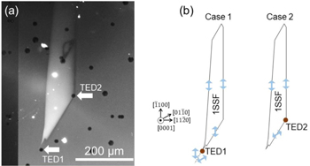
Fig. 6. (Color online) Two possibilities of conversion point from BPD to TED: (a) PL images (420 nm BPF) with two possible candidate TEDs, (b) schematic illustrations of the two possible cases.
Download figure:
Standard image High-resolution image
Fig. 7. (Color online) Burgers vector analysis of two PDs accompanying TED2: (a) SEM image and plan-view TEM sampling position, (b) plan-view TEM image with low magnification, (c) g · b contrast analysis result for PD2, and (d) g · b contrast analysis result for PD1.
Download figure:
Standard image High-resolution image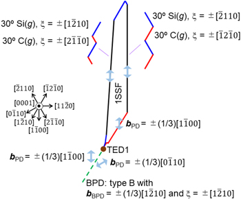
Fig. 8. (Color online) Schematic summary of structural data of the bar-shaped 1SSF, BPD at the origin, and the converted TED.
Download figure:
Standard image High-resolution image
4. Conclusions
A bar-shaped 1SSF was structurally analyzed. It was found that the terminating sides both near the epilayer surface and near the substrate/epilayer interface have the same combination of PDs, namely, 30° Si(g) and 30° C(g) PDs. More precisely, these combinations were 30° Si(g) with ξ = [1 ] and 30° C(g) with ξ = [2
 ] near the substrate/epilayer interface, and 30° Si(g) with ξ = [
 ] and 30° C(g) with ξ = [
 ] near the epilayer surface. According to the above analysis and the dislocation loop model, it was found that this 1SSF expanded toward the epilayer surface from a type B and perfect screw BPD and converted to a TED located near the substrate/epilayer interface, with
b
BPD = ±(1/3)[1
] near the epilayer surface. According to the above analysis and the dislocation loop model, it was found that this 1SSF expanded toward the epilayer surface from a type B and perfect screw BPD and converted to a TED located near the substrate/epilayer interface, with
b
BPD = ±(1/3)[1 ].
].