Interface Behaviour and Work Function Modification of Self-Assembled Monolayers on Sn-Doped In2O3


Department of Materials and Earth Sciences, Technische Universität Darmstadt, Otto-Berndt-Straße 3, 64287 Darmstadt, Germany
*
Author to whom correspondence should be addressed.
Surfaces 2019, 2(2), 241-256; https://doi.org/10.3390/surfaces2020019
Submission received: 11 March 2019
/
Accepted: 25 March 2019
/
Published: 29 March 2019
Abstract
:The modification of the work function of Sn-doped In2O3 (ITO) by vacuum adsorption of 4-(Dimethylamino)benzoic acid (4-DMABA) has been studied using in situ photoelectron spectroscopy. Adsorption of 4-DMABA is self-limited with an approximate thickness of a single monolayer. The lowest work function obtained is eV, enabling electron injection into many organic materials. In order to identify a potential influence of the ITO substrate surface on the final work function, different ITO surface orientations and treatments have been applied. Despite the expected differences in substrate work function and chemical bonding of 4-DMABA to the substrate, no influence of substrate surface orientation is identified. The resulting work function of ITO/4-DMABA substrates can be described by a constant ionization potential of the adsorbed 4-DMABA of eV, a constant band alignment between ITO and 4-DMABA and a varying Fermi energy in the ITO substrate. This corresponds to the behaviour of a conventional semiconductor heterostructure and deviates from the vacuum level alignment of interfaces between organic compounds. The difference is likely related to a stronger chemical bonding at the ITO/4-DMABA interface compared to the van der Waals bonding at interfaces between organic compounds.
1. Introduction
Tin-doped indium oxide (ITO) is often used as transparent anode material in organic optoelectronic applications like organic light emitting diodes or photovoltaics [1,2,3,4,5,6,7]. Highly efficient carrier injection and/or extraction from the transparent conducting oxide (TCO) into the organic is required, which depends on the work function of the electrode. It is therefore, desirable to control the contact properties ideally by an adjustable work function. The modification of the work function of transparent ITO electrodes has therefore, been widely investigated [6,8,9,10,11,12,13,14,15,16,17,18,19,20,21,22].
Another approach for modifying the work function is the formation of self-assembling monolayers (SAM), which utilize the self-limited adsorption of organic molecules [23,24]. Several different molecular classes have been investigated in literature, e.g., thiols, phosphonates or carboxylic acids. The molecules forming SAMs consist of an anchor group which binds to the substrate, a spacer and the head group. In particular the head group may be customized to alter the molecular dipole to effectively change the electrode work function.
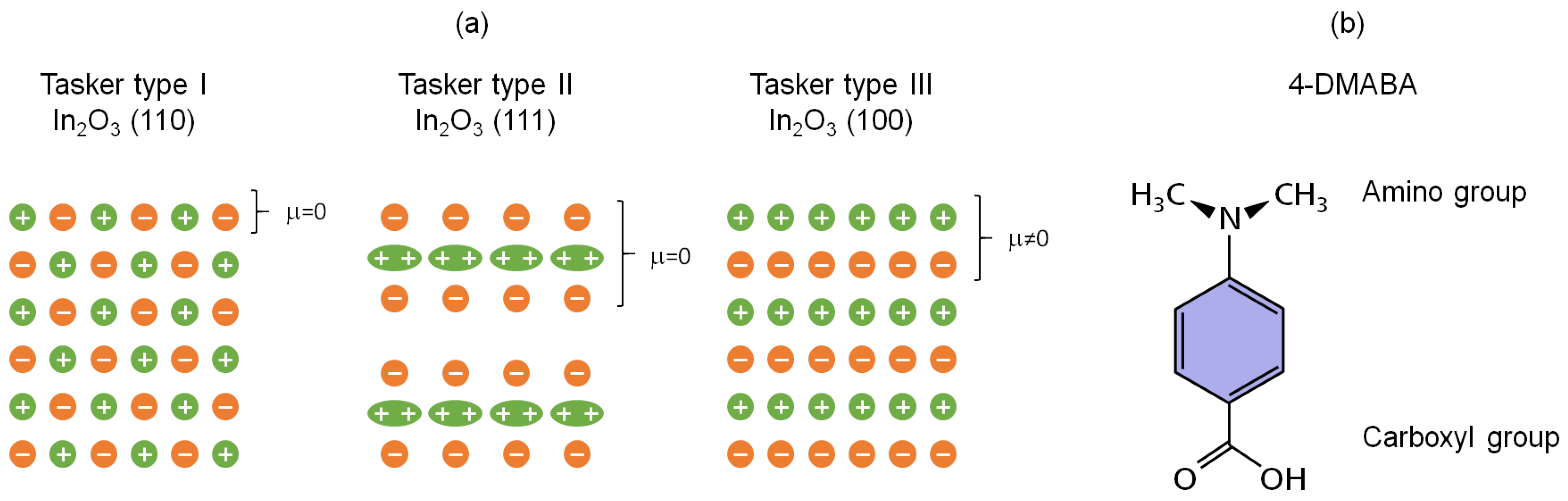
Next to the composition of the anchor group, the atomic arrangement at the electrode surface, its termination and possible adsorbates, determine the chemical bonds formed between the SAM and substrate. Regarding surface properties, surfaces of polar materials, such as indium oxide and ITO, can be classified into three types according to Tasker et al. [25]. In the case of In2O3, the -, - and -surfaces represent the basic Tasker types I–III, without polarity, with dipole-free O-In-O units and with a polar termination, respectively (see Figure 1). These surface have been investigated both theoretically and experimentally concerning surface reconstructions and stability [26,27,28,29,30,31,32,33]. For sputtered indium oxide films it was found that the surface is the most stable one over a wide range of oxygen partial pressures [29]. Significant difference of the ionization potential , which is the difference between the valence band maximum and vacuum energy, between the and -surfaces of In2O3 could be observed as well [29]. The situation is more complex for doped In2O3 due to dopant segregation [30,34,35,36].
Some authors [17,37] suggested that a surface treatment of the substrate may enhance the stability of the organic molecules. Especially the role of OH surface coverage is thought to be important for the attachment of the SAM. If solution based approaches for the SAM deposition or ITO films exposed to ambient air before functionalization are used, a high OH coverage can be assumed, while it is not that clear for a vapour phase deposition of the SAM. A surface functionalisation by a vapour phase deposition technique may be beneficial in terms of in-line device production. An activation of the surface by Ar-ion bombardment and thereby formation of a high density of reaction sites is discussed as well.
The alignment of electronic orbitals between organic molecules is generally discussed in terms of a vacuum level alignment, which can be modified by charge transfer dipoles [38,39,40]. The situation is similar to that of the band alignment between van der Waals surfaces of 2-dimensional layered chalcogenides [41]. If alignment of the vacuum level governs band alignment, a modification of the work function of the substrate should change band alignment. For ITO/organic interfaces, this behaviour has been explicitly demonstrated for example by Kugler et al. [8]. Interfaces between inorganic compounds are, on the other hand, governed by charge neutrality levels of induced gap states in the case of more covalently bonded materials [42,43], which results in the well-known Fermi level pinning. For materials with more ionic bonds, such as oxides and chalcogenides, it has been shown that the band alignment, in particular the valence band discontinuity , can be rationalized by considering the orbital contributions to the valence bands [44,45,46,47]. For inorganic compounds, the energy band alignment is quite insensitive to the work function modifications of the substrate.
The influence of substrate surface condition (including work function) on the energy level alignment and resulting work function modification of inorganic compounds by SAMs is less well studied. In the present work 4-(Dimethylamino)benzoic acid (4-DMABA, see Figure 1b) was used for the work function modification of ITO thin films. The carboxyl group is expected to bind to the surface, while the amino group should determine the change of work function [13,37,48]. All film depositions and characterization of surface composition and potentials using photoelectron spectroscopy were carried out in a single integrated UHV cluster tool. Radio frequency magnetron sputtering was applied for deposition of the ITO while 4-DMABA was deposited via the gas phase by thermal evaporation. Polycrystalline ITO films grown on quartz glass, treated by Ar-ion bombardment, oxygen plasma or exposure to H2O vapor and oriented ITO films grown on , and yttria stabilized zirconia (YSZ) single crystals were used for the adsorption of the organic molecules. The structure and the surface of the oriented films were investigated by X-ray diffraction (XRD), atomic force microscopy (AFM) and scanning electron microscopy (SEM). X-ray and ultra violet photoelectron spectroscopy (XPS and UPS) were applied to monitor the surface potentials.
2. Experimental
Thin film deposition, treatment and analysis by photoelectron spectroscopy (PES) were performed in the DArmstadt Integrated SYstem for MATerials research (DAISY-MAT), an ultra high vacuum cluster tool combining several vacuum chambers for thin film deposition and treatment and a Physical Electronics PHI 5700 (Physical Electronics, Inc., Chanhassen, MN, USA) multi-technique surface analysis system [32]. Sample preparation and surface analysis could therefore, be conducted without breaking the vacuum, assuring that no unintentional adsorbates affect the measurement signals.
ITO films were deposited on various substrates by RF magnetron sputtering from a ceramic ITO target containing wt.% SnO2. Zirconium dioxide single crystals stabilized with 8 mol% Yttrium oxide (YSZ) were used for oriented growth of ITO. -, - and -oriented single crystals with dimensions of were obtained from Alineason (Frankfurt, Germany). Deposition conditions as reported by Hohmann et al. [29] were applied. Films were deposited simultaneously on substrates of all three orientations either under reducing or oxidizing conditions, i.e., using either pure Argon or a 10% Oxygen/90% Argon process gas mixture. Polycrystalline ITO films were grown on fused silica substrates, at a power of , a target to substrate distance of , a pressure of , under reducing or oxidizing conditions and either not intentionally heated or at a substrate temperature of . The crystallographic structure of the ITO films grown on YSZ was investigated using X-ray diffraction in and in some cases in rocking curve geometry. Atomic force (AFM) and scanning electron (SEM) microscopy were used to analyze surface roughness and topography.
A wider range of ITO surface properties was achieved by treating selected samples either by Ar-ion etching, exposing to O2-plasma or H2O vapor. An area of was bombarded by Ar+ for at an acceleration voltage of , resulting in a current of . For the oxygen plasma treatment a Atom/Ion Hybrid Plasma source GenII by tectra was used. The atom mode was utilized for at a pressure of , a distance of and a current of . For the water exposure purified water was used and dosed by a special valve specified for atomic layer deposition. The samples were exposed to 25 cycles of H2O vapor, which consist of opening the valve to the water source for followed by pumping time.
The organic molecule 4-DMABA was purchased from Sigma-Aldrich (Munich, Germany) with a purity of 99%. Custom made effusion cells using resistively heated alumina crucibles were used for their evaporation. The distance between the opening of the crucibles and the sample was . The base pressure of the deposition chamber was . Evaporation of the molecules was performed at , resulting in a pressure of about during deposition. The deposition time was controlled by rotation of the sample holder.
The photoelectron spectrometer is equipped with a monochromatic Al K X-ray source and a Helium gas discharge lamp. The former was used to measure the X-ray photoelectron spectra with a photon energy of , while the latter was used for recording ultra violet photoelectron spectra in a state where the He-I emission line with a photon energy of is dominating. A sputter cleaned silver foil was used as reference to calibrate the binding energies, which are given with respect to the Fermi energy. Core levels of the present elements i.e., , , , and as well as valence band spectra were measured by XPS. The core level spectra were evaluated according to the binding energy, peak shape and integral area to obtain information of the chemical environment and to extract the composition of the samples.
A bias of was applied between sample holder and spectrometer during UPS measurements, which were performed in normal emission. The whole accessible energy range was recorded, i.e., the valence band region including the secondary electron cutoff . From the position of the secondary electron cutoff the work function can be extracted according to . Due to changes of the valence band structure upon adsorption, the band bending changes at the ITO surface induced by the different surface treatments are extracted from the binding energy of the core level. In order to reduce uncertainties of the surface potentials originating from the combination of two different excitation sources, the values for the work function discussed in this work are extracted from a combination of XP and UP spectra according to , where the ionization potential is derived from the UPS measurement .
3. Results and Discussion
3.1. Oriented ITO Films
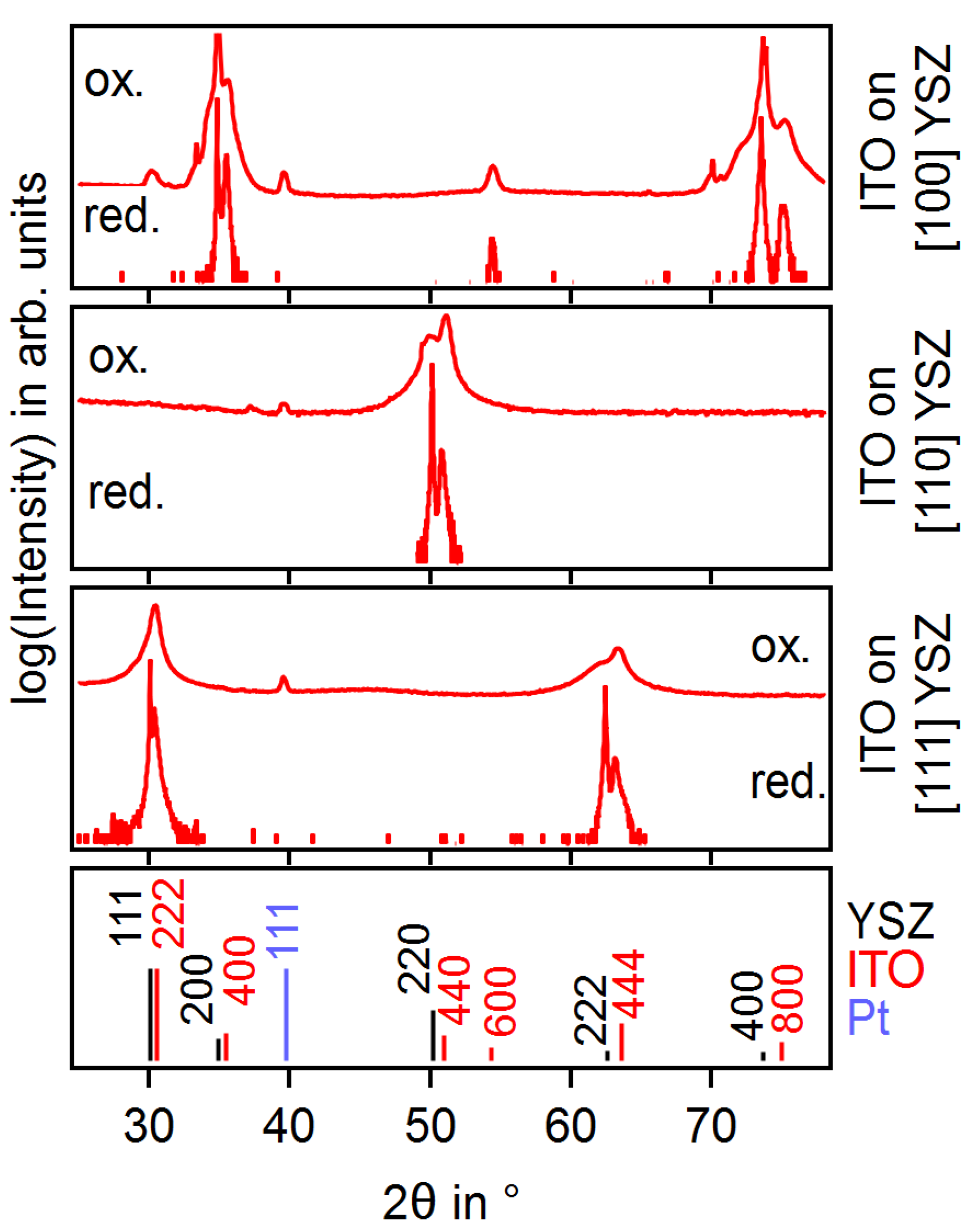
X-ray diffraction measurements of the ITO films grown under oxidizing and reducing conditions on different substrate orientations are shown in Figure 2.
Due to the ITO film thickness of less then , both substrate and film reflections can be seen. The reflection at , which is observed for the samples deposited under oxidizing conditions, is related to Pt and originates from contacts which were deposited at the corners of the samples for conductivity measurements. All other reflections can be assigned either to YSZ or to ITO. Cu K radiation causes the appearance of ghost lines at lower angles than the main reflection. The full width at half maximum (FWHM) of the rocking curves of the 200, the 220 and the 222 reflections (not shown) are all below . The mosaicity is therefore, considered as negligible, confirming oriented growth under the given conditions for all three surface orientations.
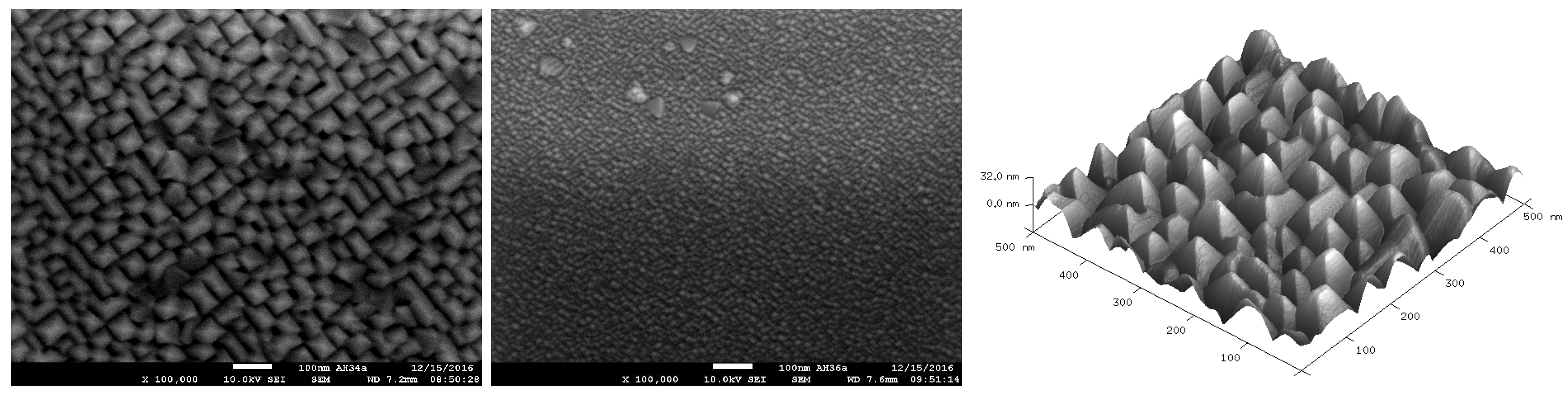
SEM and AFM images of the films grown on - and -oriented YSZ (not shown) indicate homogeneous and smooth surfaces with a roughness below . For the films grown on the -oriented substrates a distinct structure can be seen as shown in Figure 3. Under reducing conditions all grains exhibit a rectangular shape with the grain boundaries aligned at an angle of relative to the substrate edges and a pyramidal shape. The grain size of the film grown under oxidizing conditions is much smaller, making it difficult to analyze the shape in this case. However, the orientation of the grains relative to the substrate edges suggests a similar structure than for the film deposited under reducing conditions.
The pyramidal shape of the grains is confirmed by AFM measurements, which are shown at the right of Figure 3. The angle of the pyramidal faces relative to the substrate surface is derived using line scans to be ∼54. This coincides with the angle between and planes of the cubic lattice system. The orientation of the pyramidal base plane with respect to the sample edges is also consistent with the formation of surface facets. This observation corresponds well with the fact that the surface of ITO has the highest surface energy [28,30]. It is also reasonable that the surface stabilizes by exposing the lowest energy surface orientation. Unfortunately, we could not yet identify any deposition conditions to stabilize the surface orientation, rendering an assessment of the modification of this surface orientation impossible at present.
3.2. ITO Surface Potentials
The surface potentials of ITO depend on deposition conditions and surface treatment [20]. Generally, the work function of a material is affected by changes of either the Fermi energy with respect to the band edges, , or the surface dipole, which affects the ionization potential . To monitor changes of the surface dipole it is therefore, necessary to take the Fermi energy and the work function or the ionization potential into account.
Values for ITO surface potentials, which were measured after different surface treatments, are given in Table 1. As some surfaces were specially treated, those values are shown as well. The values for the Fermi energy, ionization potential and work function of the as-deposited ITO films vary between 2.4–3.1 , 7.3–7.8 and 4.5–5.0 , respectively. The influence of the deposition parameters on these values were already reported earlier [20] and are in good agreement with the data given in Table 1.
The highest Fermi energies and, correspondingly, the lowest work functions were measured on samples, which were deposited in a pure Argon atmosphere and at substrate temperature. Oxygen in the process atmosphere results in a lower Fermi energy and a higher work function, but has no effect on the ionization potential, in agreement with previous studies [34,49,50].
Samples 1–9 in Table 1 were deposited from a heavily used ITO target with a deep race track. A new target of the same composition, from the same manufacturer and batch was used for the remaining samples. Comparing films 9 and 10, which were deposited onto unheated substrates, the film prepared from new target exhibits a lower Fermi energy ( as compared to from the old target), indicating a higher oxygen content in the film due to a more oxygen-rich target. The films deposited in pure Ar from the new target have even lower Fermi energies than the films deposited with oxygen from the old target (sample 7). The lower ionization potentials of the samples deposited at room temperature from the new target could be related to a different surface orientation, which has been observed to affect the ionization potential of room temperature deposited ITO films [32].
Oxidative post deposition treatments are known to increase the ionization potential and the work function of ITO films [9,20,51,52]. Sample 8, which was deposited at room temperature and then annealed at in O for 1 h, already exhibits a high ionization potential of after this treatment, which is not further increased by the oxygen plasma treatment. However, the oxygen plasma treatment substantially lowers the Fermi energy and therefore, increases the work function of this sample.
Slightly reduced ionization potentials are observed after Ar-ion etching and after exposure to water vapor. The Fermi energy is slightly raised after these treatments. The ionization potential of the deposited ITO films does not depend on the orientation of the films. In the case of the oriented film this is very likely related to the facetting of the surface described above. Nevertheless, according to DFT calculations [28,29,30,33], one would expect some differences between - and -oriented films, which both exhibit flat surfaces. A possible explanation for the independence on surface orientation is the segregation of the Sn dopant to the surface, which is particularly observed under reducing conditions [34,35,36]. A different surface composition will affect the surface dipole. Instead of exposing oriented InO surfaces, the actual surface composition may be SnO resulting in an ionization potential independent of orientation.
3.3. Adsorption of 4-DMABA
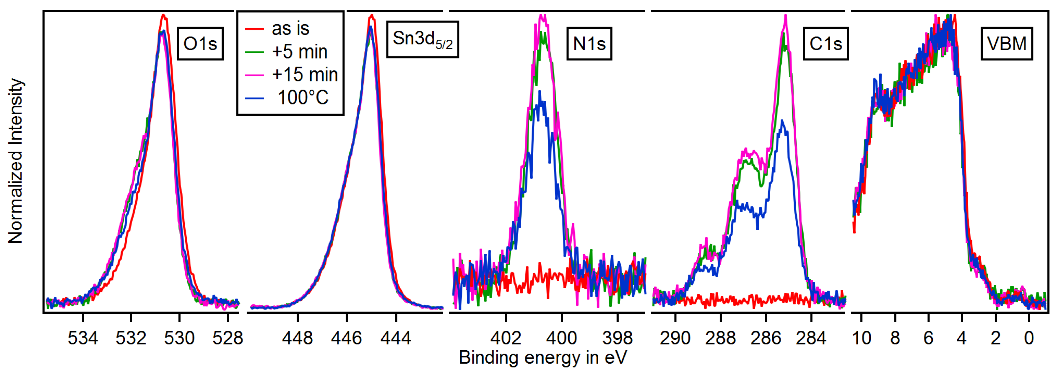
X-ray photoelectron spectra of sample 13 measured in the course of deposition of 4-DMABA are shown in Figure 4. The ITO film was grown in pure Ar at a substrate temperature of . Similar spectra are recorded for all samples listed in Table 1. A background subtraction using the Shirley-method was performed for the core levels [53,54]. For better comparison of binding energies and peak shapes, all intensities were normalized to the In 3d5/2 peak area. The valence band spectra were normalized by adjusting the maximum intensity to 1.
No carbon or nitrogen is present at the surface of the as deposited film, ensuring a contamination free surface and that the C 1s and N 1s signals after deposition of 4-DMABA are solely due to adsorption of this species. The valence band has the typical shape of ITO [34]. The emission at binding energies 2–3 and the small intensity below the Fermi energy are only observed for oxygen deficient samples [34,55]. The shape of the XPS valence bands does not change noticeably in the course of 4-DMABA deposition. This is due to the low coverage and the low photoionization cross-section of the C 2p photoelectrons [56]. The asymmetric peak shapes of the O 1s and In 3d peaks of the bare ITO film are related to screening effects of the core-hole by the conduction electrons [34,55,57].
Adsorption of 4-DMABA is indicated by the occurrence of the N 1s and C 1s emissions. While the shape of the In 3d emission of the substrate does not change upon adsorption, a shoulder appears at the high binding energy side of the O 1s. The shoulder can be assigned to the carboxyl group of the 4-DMABA molecules. The O 1s and In 3d core levels are shifted slightly to higher binding energies, which is explained by a downward band bending.
The N 1s core level emission exhibits a single component, while three components can be identified in the C 1s spectrum. According to the chemical shifts, the component with the lowest binding energy can be assigned to carbon in the benzene ring, the intermediate component to carbon bound to nitrogen and the high energy component to the carbon in the carboxyl group [10,58,59]. The intensity ratio of the three components corresponds to the ratio of carbon atoms in the benzene, the amino acid and the anchor group of 6:2:1.
The C 1s and N 1s intensities and peak shapes do not change with increasing the deposition time from 5 to 15 min. The saturation of the signals indicates a self-limited adsorption on the ITO surface and therefore, suggests the formation of a monolayer of the organic species.
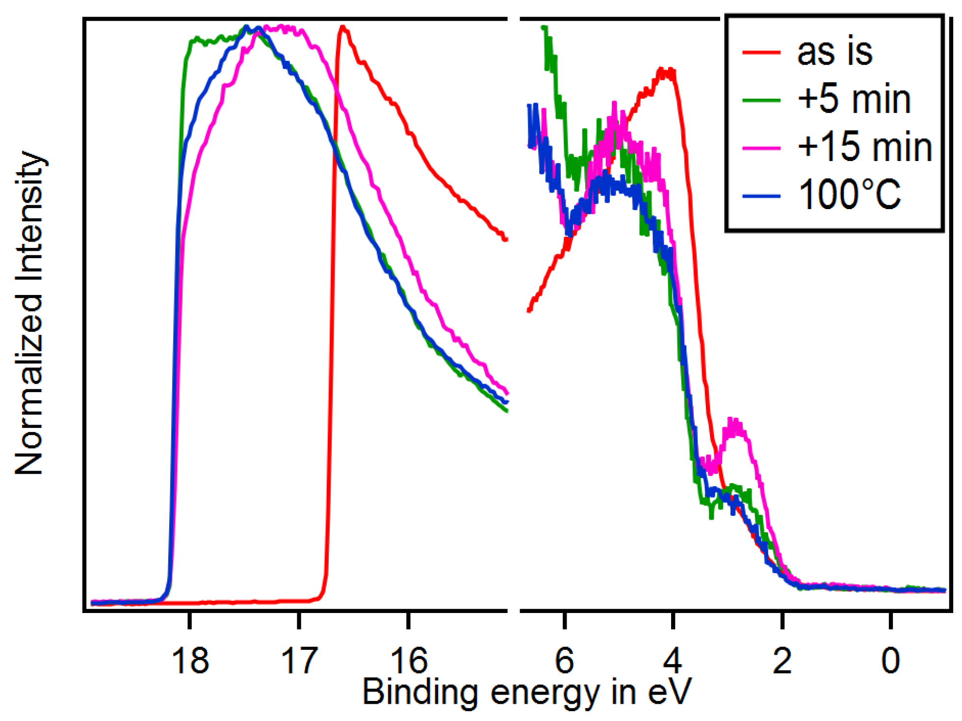
The secondary electron cutoff and the valence band region of the UP spectra are displayed in Figure 5. The spectra were normalized for better comparison. As for the XPS valence band, the spectrum of the bare ITO sample also exhibits an emission at 2–3 eV binding energy related to the oxygen deficiency [34]. In contrast to the XPS valence bands, the shape of the UPS valence band is significantly changing upon adsorption of 4-DMABA due to the higher surface sensitivity and higher photoionization cross-sections of the molecule’s valence orbitals. The new feature at low binding energies can be used to determine the highest occupied molecular orbital (HOMO) of the adsorbed molecules in a similar way as the Fermi energy is determined.
A pronounced shift of the secondary electron cutoff to higher binding energies indicates a substantial decrease of work function upon adsorption of 4-DMABA. Together with the small change of the Fermi energy, which is extracted from the XP spectra, the shift of the secondary electron cutoff and work function must be induced by a change of the surface dipole, as intended. The final position of the secondary electron cutoff is achieved after 5 min of adsorption time, indicating no impact of further adsorption on the surface dipole.
The stability of the organic molecules on the surface was tested by annealing at different temperatures in UHV. Only the spectra after the first annealing step at for 10 min with a heating rate of are shown. A slight decrease in intensity of the N 1s and C 1s peaks is observed, but the shape of the peaks is not affected (see Figure 4). This indicates that the molecules remain intact and only some desorption occurs at this temperature, which is further supported by the changes in the UPS valence band and the absence of a work function change.
Annealing at higher temperatures in UHV further decreases the intensity of the N 1s and C 1s signals but also results in a change of their peak shape, indicating a chemical decomposition of the molecules. The changes are also accompanied by a shift of the secondary electron cutoff towards the value of the bare ITO surface.
Stability tests were performed on different samples and in different vacuum chambers. The decomposition of the 4-DMABA reported above was observed when the annealing was performed in a chamber where no organic molecules have been deposited. In contrast, no changes of coverage and peak shape were observed after heating to temperatures up to when the annealing was performed in the deposition chamber of the organic molecules. Very likely, re-adsorption of organic molecules from the sample holder or the chamber walls occurs in this case, erroneously indicating a higher thermal stability of the molecules.
3.4. Dependence on Surface Orientation and Treatment
In order to study the effect of different surface conditions of ITO onto the adsorption of 4-DMABA, oriented and polycrystalline ITO films were deposited under reducing or oxidizing process atmospheres. Some of the polycrystalline samples were treated after the deposition either by oxygen plasma, Argon ion-etching or exposure to HO vapor. All experiments were carried out within the DAISY-MAT system, i.e., without exposure of the sample to air between the different steps. As described above, the processes result in a variation of surface potentials of the ITO surface. Moreover, the surface termination itself might be altered and therefore, a different bonding of the molecules to the surface may be established.
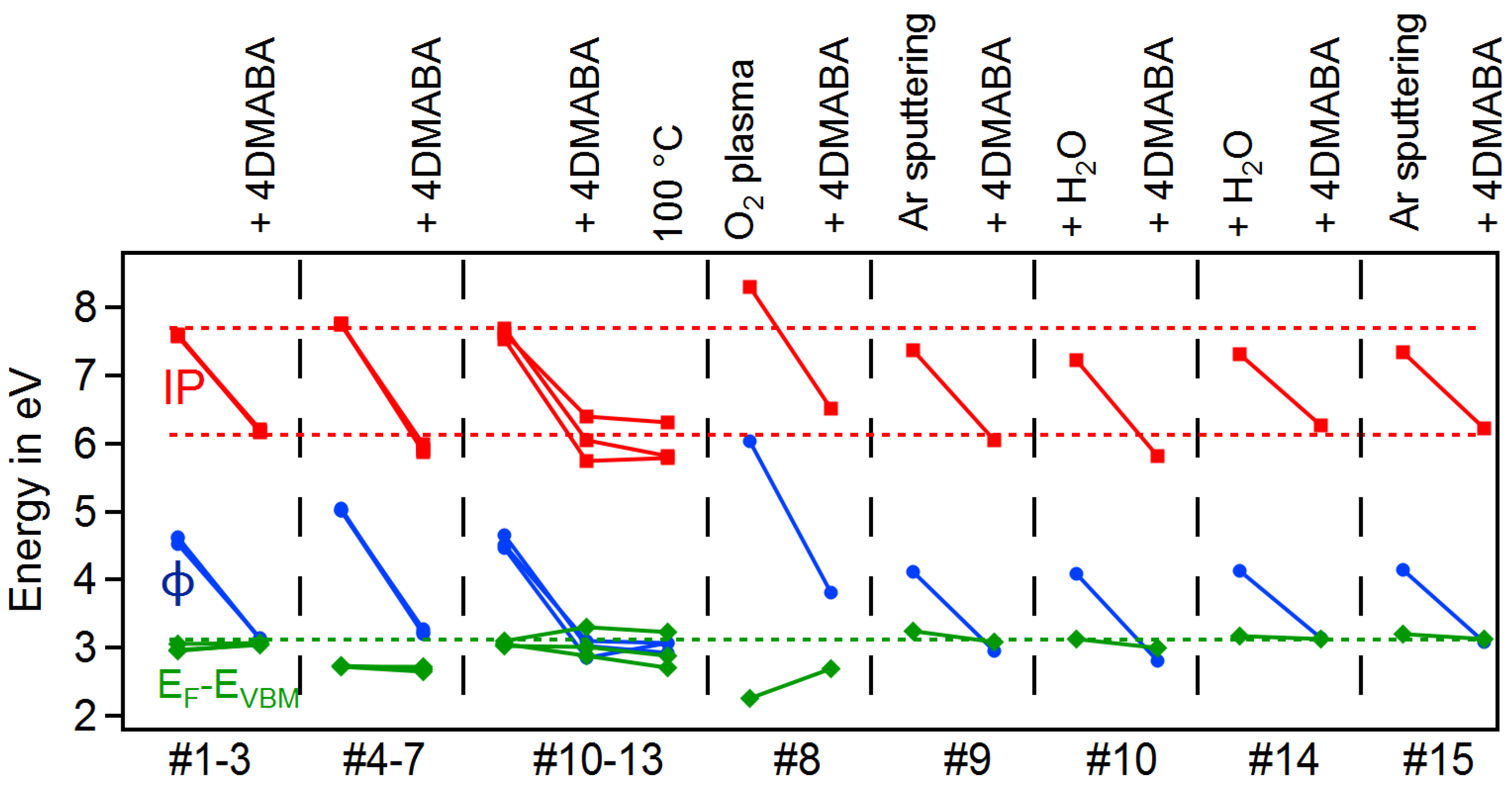
Depending on the deposition conditions, different surface potentials of the ITO thin films were obtained as listed in Table 1 and shown in Figure 6. While the ionization potentials of all untreated films grown at high temperature amount to ∼, Fermi energies and therefore, work functions are affected by the process atmosphere. Room temperature films show lower ionization potentials. A post deposition treatment leads to both, a change of and Fermi energy.
Starting from the conditions given in Table 1, 4-DMABA adsorption experiments were carried out. It is observed that the adsorption behaviour is not affected by the initial film condition. Identical intensities, peak shapes and similar binding energies are observed for all samples. Regarding the stability of the molecules on the surfaces, also no dependence on surface treatment was observed. The decomposition started above for all samples.
The presence of a hydroxyl termination of the substrate surface is often discussed as essential for the formation of a SAM [11,13,17,52,60]. In this work all films were grown, treated and analysed within the DAISY-MAT system without breaking vacuum. Moreover, ITO deposition, treatment and organic molecule adsorption were all performed consecutively without delay within one day. While the formation of a hydroxyl termination of the ITO surface by outgasing of Hydrogen from the stainless steel vacuum chambers cannot be excluded [61], the OH coverage on the ITO surfaces is considered to be rather low. Only after exposure to H2O vapor do we expect a complete coverage of the ITO surface with OH groups. In this case, a shoulder at the high binding energy side of the O 1s peak appears, which indicates a hydroxyl termination. It has also been pointed out that XPS measurements do not give direct evidence for the presence of OH groups [52]. Such uncertainties are, however, less pronounced in the present case as compared to ex-situ studies of chemically treated surfaces, where a multitude of surface species can contribute to the shoulder in the O 1s emission. No significant difference in coverage or stability of 4-DMABA of the water exposed surface could be observed. This indicates that a substantial OH coverage is not decisive for the adsorption of the chosen molecules, which is consistent with the independence on surface orientation and treatment.
The surface potentials after adsorption of 4-DMABA are included in Figure 6. Fermi energies are hardly affected by the adsorption of the molecules with exception of the room temperature films, which show a slightly larger shift. Therefore, no significant electron transfer between ITO and 4-DMABA occurs.
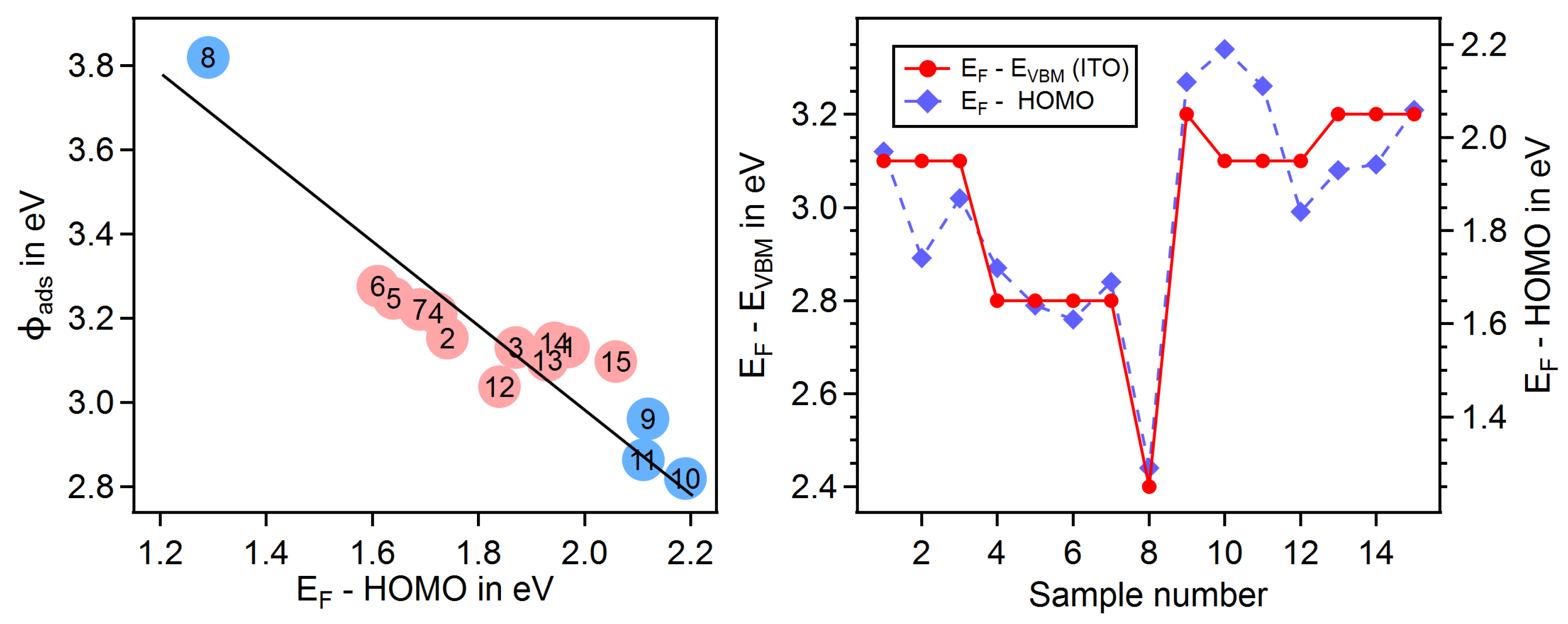
A comparison of the work functions of the films after adsorption to the HOMO energy of the 4-DMABA molecules is shown in Figure 7 (left). Work functions of the samples obtained from ITO films deposited at high temperature are very similar with a variation of ∼. Including samples deposited at room temperatures the total variation of the work function after adsorption amounts to . It is evident, however, that the work function after adsorption is linearly related to the HOMO position. This is indicated by the fit in the left graph of Figure 7, which exhibits a slope of . Consequently, the ionization potential of the organic molecule is constant with a value of and the variation of the work function after adsorption is only caused by a variation of the Fermi energy. Such a behaviour would be reasonable for adsorbed species with weak chemical interaction with the substrate as for interfaces between organic molecules [38,39,40]. In the case of chemically bound SAMs, such a behaviour is not necessarily expected due to the modification of the electronic structure of the molecule.
The HOMO energies and Fermi level positions in ITO after adsorption are shown for all samples in the right graph of Figure 7. The Fermi energies in ITO are not straightforward to extract from the spectra due to different binding energy shifts of the various levels [34,55]. Consistent values could only be derived considering UPS and XPS valence band and In 3d5/2 core level spectra together. The two energy axis in the right graph of Figure 7 for the HOMO level of the 4-DMABA (right axis) and the valence band maximum for ITO (left axis) span . In spite of different absolute values, both energies follow the same trend. The mean value of the difference between both energies amounts to . The constant difference between the ITO valence band maximum and the HOMO of 4-DMABA indicates a fixed constant energy band alignment between the two materials. In other words, the variation of the work function of the ITO/4-DMABA is only determined by the variation of the Fermi energy in the ITO substrate. The work function of ITO before adsorption does not determine the work function after adsorption. This is different from the reported behaviour that the energy band alignment between ITO and organic molecules can be modified by manipulating the ITO work function [8].
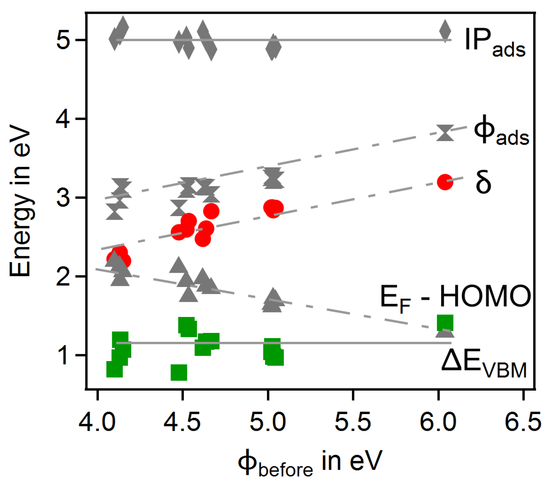
The different values related to the formation of the ITO/4-DMABA interface and the resulting work function of the samples are plotted in Figure 8 vs. the work function of the ITO substrate before adsorption. As already outlined above, the ionization potential and the valence band discontinuity are independent of the ITO work function. The work function and the Fermi energy show opposite trends. The interface dipole potential also increases with the work function of the substrate, which is another way to display that the work function after adsorption does not depend on the ITO work function before adsorption.
Kugler et al. [8], who investigated the band alignment between organic polymers and differently treated ITO surfaces, used a plot similar to the one shown in Figure 8. In contrast to the behaviour of the ITO/4-DMABA interface, their interfaces exhibit a constant interface dipole potential , indicating a vacuum level alignment between ITO and the polymer layer. The latter behaviour therefore, confirms that the band alignment between ITO and 4-DMABA is determined by adjustment between the valence band maximum in the ITO and the HOMO level in 4-DMABA.
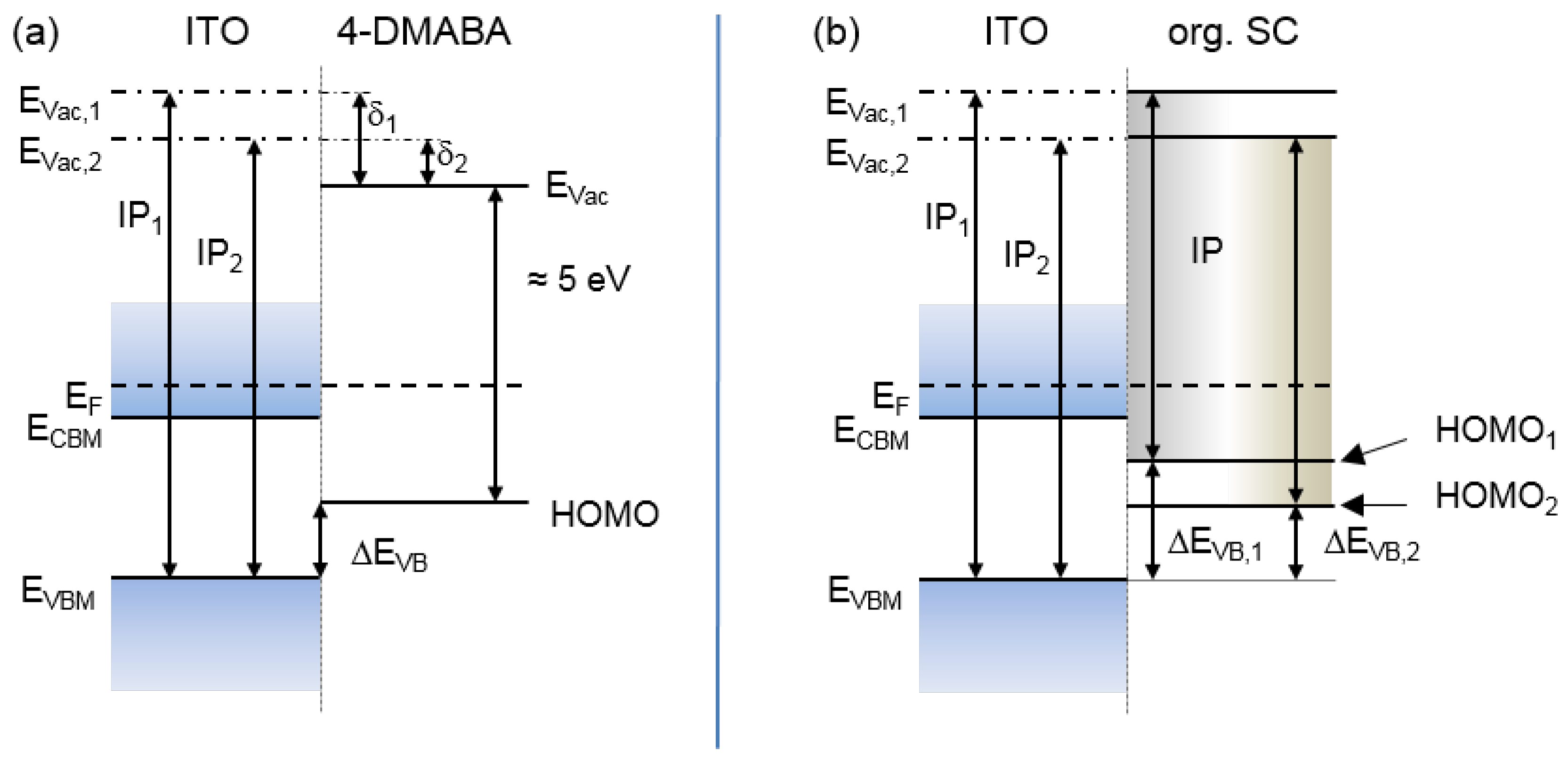
Schematic energy band diagrams showing the variation of energy band alignment for the ITO/4-MDABA interface are shown in Figure 9a. A different ionization potential of the ITO substrate is compensated by a different interface dipole potential . As a consequence, the distance between the ITO valence band maximum and the HOMO of the 4-DMABA, is independent of the ITO ionization potential and work function. The band alignment in the case of a vacuum level alignment as reported for most inorganic/organic interfaces is shown in Figure 9b. In this case, the interface dipole potential is negligible and the offset depends on the substrate conditions.
4. Summary and Conclusions
The interface formation of 4-(Dimethylamino)benzoic acid and Sn-doped In2O3 has been studied using in situ photoelectron spectroscopy. ITO films were prepared by magnetron sputtering with different surface orientation on single crystalline Y-stabilized ZrO and with polycrystalline structure on quartz glass. Different surface treatments before adsorption of 4-DMABA have been applied. The work function of ITO before adsorption varied by more than 1 eV for the different treatments.
Adsorption of 4-DMABA was carried out by thermal evaporation. A self-limited adsorption behaviour was observed, indicating formation of a self-assembled monolayer. The layers are stable upon heating in vacuum up to C. Higher temperatures resulted in chemical decomposition of the molecules.
The work function of the ITO is substantially reduced to values as low as 2.82 eV. No dependence on surface orientation is observed. The energy band alignment at the ITO/4-DMABA interface is characterized by a constant ionization potential of and a constant energy difference between the ITO valence band maximum and the HOMO of 4-DMABA of . This type of band alignment is characteristic for interfaces between inorganic semiconductors and differs from the vacuum level alignment typically observed for interfaces between organic semiconductors.
The variation of the work function after adsorption amounts to ∼eV. The variation is caused by a variation of the Fermi energy in the ITO substrate. Oxidizing conditions during ITO preparation result, in particular for room temperature preparation, in low Fermi energies and consequently to high work functions. Lowest work functions are obtained for room temperature deposited ITO films which were exposed to reducing surface treatments. For typical ITO surface conditions, such as observed after high-temperature deposition without further treatment, the work can be reduced to eV.
Author Contributions
Thin film deposition and interface analysis was peformed by A.H.H., scanning probe microscopy by D.D. and X-ray diffraction by J.B. Discussion and interpretation of results was conducted by A.H.H. and A.K. Manuscript was written by and A.H.H. and A.K. and revised by all authors; Funding has been acquired by A.K.
Funding
This work was supported by the German Federal Ministry for Education and Research (BMBF), contract number 13N13704.
Conflicts of Interest
The authors declare no conflict of interest. The founding sponsors had no role in the design of the study; in the collection, analyses, or interpretation of data; in the writing of the manuscript, and in the decision to publish the results.
Abbreviations
The following abbreviations are used in this manuscript:
| 4-DMABA | 4-(Dimethylamino)benzoic acid |
| ITO | Sn-doped In2O3 |
| YSZ | Y-stabilized zirconia (ZrO:Y) |
| HOMO | higher occupied molecular orbital |
| VBM | valence band maximum |
| SAM | self-assembled monolayer |
| XPS | X-ray photoelectron spectroscopy |
| UPS | ultraviolet photoelectron spectroscopy |
| XRD | X-ray diffraction |
| AFM | atomic force microscopy |
| SEM | scanning electron microscopy |
References
- Cui, J.; Wang, A.; Edleman, N.L.; Ni, J.; Lee, P.; Armstrong, N.R.; Marks, T.J. Indium tin oxide alternatives—High work function transparent conducting oxides as anodes for organic light-emitting diodes. Adv. Mater. 2001, 13, 1476–1480. [Google Scholar] [CrossRef]
- Marks, T.J.; Veinot, J.G.C.; Cui, J.; Yan, H.; Wang, A.; Edleman, N.L.; Ni, J.; Huang, Q.; Lee, P.; Armstrong, N.R. Progress in high work function TCO OLED anode alternatives and OLED nanopixelation. Synth. Met. 2002, 127, 29–35. [Google Scholar] [CrossRef]
- Schulze, K.; Maennig, B.; Leo, K.; Tomita, Y.; May, C.; Hüpkes, J.; Brier, E.; Reinold, E.; Bäuerle, P. Organic solar cells on indium tin oxide and aluminum doped zinc oxide anodes. Appl. Phys. Lett. 2007, 91, 073521. [Google Scholar] [CrossRef]
- Fortunato, E.; Ginley, D.; Hosono, H.; Paine, D.C. Transparent conducting oxides for photovoltaics. MRS Bull. 2007, 32, 242–247. [Google Scholar] [CrossRef]
- Klein, A.; Körber, C.; Wachau, A.; Säuberlich, F.; Gassenbauer, Y.; Harvey, S.P.; Proffit, D.E.; Mason, T.O. Transparent Conducting Oxides for Photovoltaics: Manipulation of Fermi Level, Work Function, and Energy Band Alignment. Materials 2010, 3, 4892–4914. [Google Scholar] [CrossRef] [PubMed]
- Armstrong, N.R.; Veneman, P.A.; Ratcliff, E.; Placencia, D.; Brumbach, M. Oxide Contacts in Organic Photovoltaics: Characterization and Control of Near-Surface Composition in Indium-Tin Oxide (ITO) Electrodes. Acc. Chem. Res. 2009, 42, 1748–1757. [Google Scholar] [CrossRef] [PubMed]
- Cao, W.R.; Li, J.; Chen, H.Z.; Xue, J.G. Transparent electrodes for organic optoelectronic devices: A review. J. Photonics Energy 2014, 4, 040990. [Google Scholar] [CrossRef]
- Kugler, T.; Salaneck, W.R.; Rost, H.; Holmes, A.B. Polymer band alignment at the interface with indium tin oxide: Consequences for light emitting diodes. Chem. Phys. Lett. 1999, 310, 391–396. [Google Scholar] [CrossRef]
- Mason, M.G.; Hung, L.S.; Tang, C.W.; Lee, S.T.; Wong, K.W.; Wang, M. Characterization of treated indium-tin-oxide surfaces used in electroluminescent devices. J. Appl. Phys. 1999, 86, 1688–1692. [Google Scholar] [CrossRef]
- Yan, C.; Zharnikov, M.; Golzhauser, A.; Grunze, M. Preparation and characterization of self-assembled monolayers on indium tin oxide. Langmuir 2000, 16, 6208–6215. [Google Scholar] [CrossRef]
- Purvis, K.L.; Lu, G.; Schwartz, J.; Bernasek, S.L. Surface characterization and modification of indium tin oxide in ultrahigh vacuum. J. Am. Chem. Soc. 2000, 122, 1808–1809. [Google Scholar] [CrossRef]
- Span, A.R.; Bruner, E.L.; Bernasek, S.L.; Schwartz, J. Surface modification of indium tin oxide by phenoxytin complexes. Langmuir 2001, 17, 948–952. [Google Scholar] [CrossRef]
- Carrara, M.; Nüesch, F.; Zuppiroli, L. Carboxylic acid anchoring groups for the construction of self-assembled monolayers on organic device electrodes. Synth. Met. 2001, 121, 1633–1634. [Google Scholar] [CrossRef]
- Donley, C.; Dunphy, D.; Paine, D.; Carter, C.; Nebesny, K.; Lee, P.; Alloway, D.; Armstrong, N.R. Characterization of Indium-Tin Oxide Interfaces Using X-ray Photoelectron Spectroscopy and Redox Processes of a Chemisorbed Probe Molecule: Effect of Surface Pretreatment Conditions. Langmuir 2002, 18, 450–457. [Google Scholar] [CrossRef]
- Hsu, C.M.; Wu, W.T. Improved characteristics of organic light-emitting devicesby surface modification of nickel-doped indium tin oxide anode. Appl. Phys. Lett. 2004, 85, 840–842. [Google Scholar] [CrossRef]
- Lägel, B.; Beerbom, M.M.; Doran, B.V.; Lägel, M.; Cascio, A.; Schlaf, R. Investigation of the poly[2-methoxy-5-(2’-ethyl-hexyloxy)-1,4-phenylene vinylene]/indium tin oxide interface using photoemission spectroscopy. J. Appl. Phys. 2005, 98, 023512. [Google Scholar] [CrossRef]
- Bermudez, V.M.; Berry, A.D.; Kim, H.; Pique, A. Functionalization of indium tin oxide. Langmuir 2006, 22, 11113–11125. [Google Scholar] [CrossRef]
- Brumbach, M.; Veneman, P.A.; Marrikar, F.S.; Schulmeyer, T.; Simmonds, A.; Xia, W.; Lee, P.; Armstrong, N.R. Surface Composition and Electrical and Electrochemical Properties of Freshly Deposited and Acid-Etched Indium Tin Oxide Electrodes. Langmuir 2007, 23, 11089–11099. [Google Scholar] [CrossRef]
- Kim, H.; Sohn, S.; Jung, D.; Maeng, W.J.; Kim, H.; Kim, T.S.; Hahn, J.; Lee, S.; Yi, Y.; Cho, M.H. Improvement of the contact resistance between ITO and pentacene using various metal-oxide interlayers. Org. Electron. 2008, 9, 1140–1145. [Google Scholar] [CrossRef]
- Klein, A.; Körber, C.; Wachau, A.; Säuberlich, F.; Gassenbauer, Y.; Schafranek, R.; Harvey, S.P.; Mason, T.O. Surface potentials of magnetron sputtered transparent conducting oxides. Thin Solid Films 2009, 518, 1197–1203. [Google Scholar] [CrossRef]
- Hotchkiss, P.J.; Jones, S.C.; Paniagua, S.A.; Sharma, A.; Kippelen, B.; Armstrong, N.R.; Marder, S.R. The Modification of Indium Tin Oxide with Phosphonic Acids: Mechanism of Binding, Tuning of Surface Properties, and Potential for Use in Organic Electronic Applications. Acc. Chem. Res. 2012, 45, 337–346. [Google Scholar] [CrossRef] [PubMed]
- Rittich, J.; Jung, S.; Siekmann, J.; Wuttig, M. Indium-Tin-Oxide (ITO) Work Function Tailoring by Covalently Bound Carboxylic Acid Self-Assembled Monolayers. Phys. Status Solidi (b) 2018, 255, 1800075. [Google Scholar] [CrossRef]
- Heimel, G.; Romaner, L.; Zojer, E.; Bredas, J.L. The interface energetics of self-assembled monolayers on metals. Acc. Chem. Res. 2008, 41, 721–729. [Google Scholar] [CrossRef] [PubMed]
- Würfel, U.; Seßler, M.; Unmüssig, M.; Hofmann, N.; List, M.; Mankel, E.; Mayer, T.; Reiter, G.; Bubendorff, J.L.; Simon, L.; et al. How Molecules with Dipole Moments Enhance the Selectivity of Electrodes in Organic Solar Cells—A Combined Experimental and Theoretical Approach. Adv. Energy Mater. 2016, 6, 1600594. [Google Scholar] [CrossRef]
- Tasker, P.W. The stability of ionic crystal surfaces. J. Phys. C 1979, 12, 4977. [Google Scholar] [CrossRef]
- Morales, E.H.; He, Y.; Vinnichenko, M.; Delley, B.; Diebold, U. Surface structure of Sn-doped In2O3 (111) thin films by STM. New J. Phys. 2008, 10, 125030. [Google Scholar] [CrossRef]
- Morales, E.H.; Diebold, U. The structure of the polar Sn-doped indium oxide (001) surface. Appl. Phys. Lett. 2009, 95, 253105. [Google Scholar] [CrossRef]
- Walsh, A.; Catlow, C.R.A. Structure, stability and work functions of the low index surfaces of pure indium oxide and Sn-doped indium oxide (ITO) from density functional theory. J. Mater. Chem. 2010, 20, 10438–10444. [Google Scholar] [CrossRef]
- Hohmann, M.V.; Ágoston, P.; Wachau, A.; Bayer, T.J.M.; Brötz, J.; Albe, K.; Klein, A. Orientation Dependent Ionization Potential of In2O3: A Natural Source for Inhomogeneous Barrier Formation at Electrode Interfaces in Organic Electronics. J. Phys. Condens. Matter 2011, 23, 334203. [Google Scholar] [CrossRef] [PubMed]
- Ágoston, P.; Albe, K. Thermodynamic stability, stoichiometry and electronic structure of bcc-In2O3 surfaces. Phys. Rev. B 2011, 84, 045311. [Google Scholar] [CrossRef]
- Hagleitner, D.R.; Menhart, M.; Jacobson, P.; Blomberg, S.; Schulte, K.; Lundgren, E.; Kubicek, M.; Fleig, J.; Kubel, F.; Puls, C.; et al. Bulk and surface characterization of In2O3(001) single crystals. Phys. Rev. B 2012, 85, 115441. [Google Scholar] [CrossRef]
- Klein, A. Transparent Conducting Oxides: Electronic Structure—Property Relationship from Photoelectron Spectroscopy with in situ Sample Preparation. J. Am. Ceram. Soc. 2013, 96, 331–345. [Google Scholar] [CrossRef]
- Gassmann, A.; Yampolskii, S.V.; Klein, A.; Albe, K.; Vilbrandt, N.; Pekkola, O.; Genenko, Y.A.; Rehahn, M.; von Seggern, H. Study of electrical fatigue by defect engineering in organic light-emitting diodes. Mater. Sci. Eng. B 2015, 192, 26–51. [Google Scholar] [CrossRef]
- Gassenbauer, Y.; Schafranek, R.; Klein, A.; Zafeiratos, S.; Hävecker, M.; Knop-Gericke, A.; Schlögl, R. Surface states, surface potentials and segregation at surfaces of tin-doped In2O3. Phys. Rev. B 2006, 73, 245312. [Google Scholar] [CrossRef]
- Hoyer, K.L.; Hubmann, A.H.; Klein, A. Influence of dopant segregation on the work function and electrical properties of Ge-doped in comparison to Sn-doped In2O3 thin films. Phys. Status Solidi (a) 2017, 214, 1600486. [Google Scholar] [CrossRef]
- Frischbier, M.V.; Wardenga, H.F.; Weidner, M.; Bierwagen, O.; Jia, J.; Shigesato, Y.; Klein, A. Influence of dopant species and concentration on grain boundary scattering in degenerately doped In2O3 thin films. Thin Solid Films 2016, 614, 62–68. [Google Scholar] [CrossRef]
- Nüesch, F.; Carrara, M.; Zuppiroli, L. Solution versus Vapor Growth of Dipolar Layers on Activated Oxide Substrates. Langmuir 2003, 19, 4871–4875. [Google Scholar] [CrossRef]
- Ishii, H.; Sugiyama, K.; Ito, E.; Seki, K. Energy Level Alignment and Interfacial Electronic Structures at Organic/Metal and Organic/Organic Interfaces. Adv. Mater. 1999, 11, 605–625. [Google Scholar] [CrossRef]
- Fahlman, M.; Crispin, A.; Crispin, X.; Henze, S.K.M.; de Jong, M.P.; Osikowicz, W.; Tengstedt, C.; Salaneck, W.R. Electronic structure of hybrid interfaces for polymer-based electronics. J. Phys. Condens. Matter 2007, 19, 183202. [Google Scholar] [CrossRef] [PubMed]
- Gao, Y. Surface analytical studies of interfaces in organic semiconductor devices. Mater. Sci. Eng. R 2010, 68, 39–87. [Google Scholar] [CrossRef]
- Schlaf, R.; Lang, O.; Pettenkofer, C.; Jaegermann, W. Band lineup of layered semiconductor heterointerfaces prepared by van der Waals epitaxy: Charge transfer correction term for the electron affinity rule. J. Appl. Phys. 1999, 85, 2732–2753. [Google Scholar] [CrossRef]
- Tersoff, J. Schottky barrier heights and the continuum of gap states. Phys. Rev. Lett. 1984, 52, 465–468. [Google Scholar] [CrossRef]
- Tersoff, J. Theory of semiconductor heterojunction: The role of quantum dipoles. Phys. Rev. B 1984, 30, 4874–4877. [Google Scholar] [CrossRef]
- Klein, A. Energy band alignment at interfaces of semiconducting oxides: A review of experimental determination using photoelectron spectroscopy and comparison with theoretical predictions by the electron affinity rule, charge neutrality levels, and the common anion rule. Thin Solid Films 2012, 520, 3721–3728. [Google Scholar]
- Li, S.; Morasch, J.; Klein, A.; Chirila, C.; Pintilie, L.; Jia, L.; Ellmer, K.; Naderer, M.; Reichmann, K.; Gröting, M.; et al. Influence of orbital contributions to valence band alignment of Bi2O3, Fe2O3, BiFeO3, and Bi0.5Na0.5TiO3. Phys. Rev. B 2013, 88, 045428. [Google Scholar] [CrossRef]
- Li, S.; Chen, F.; Schafranek, R.; Bayer, T.J.M.; Rachut, K.; Fuchs, A.; Siol, S.; Weidner, M.; Hohmann, M.; Pfeifer, V.; et al. Intrinsic energy band alignment of functional oxides. Phys. Status Solidi (RRL) 2014, 8, 571–576. [Google Scholar] [CrossRef]
- Klein, A. Energy Band Alignment in Chalcogenide Thin Film Solar Cells from Photoelectron Spectroscopy. J. Phys. Condens. Matter 2015, 27, 134201. [Google Scholar] [CrossRef]
- Nüesch, F.; Rotzinger, F.; Si-Ahmed, L.; Zuppiroli, L. Chemical potential shifts at organic device electrodes induced by grafted monolayers. Chem. Phys. Lett. 1998, 288, 861–867. [Google Scholar] [CrossRef]
- Gassenbauer, Y.; Klein, A. Electronic and chemical properties of ITO surfaces and ITO/ZnPc interfaces studied in situ by photoelectron spectroscopy. J. Phys. Chem. B 2006, 110, 4793–4801. [Google Scholar] [CrossRef]
- Harvey, S.P.; Mason, T.O.; Gassenbauer, Y.; Schafranek, R.; Klein, A. Surface vs. Bulk Electronic/Defect Structures of Transparent Conducting Oxides. Part I. Indium Oxide and ITO. J. Phys. D Appl. Phys. 2006, 39, 3959–3968. [Google Scholar] [CrossRef]
- Harvey, S.P.; Mason, T.O.; Körber, C.; Gassenbauer, Y.; Klein, A. Evidence for surface dipole modifications in In2O3-based transparent conductors. Appl. Phys. Lett. 2008, 92, 252106. [Google Scholar] [CrossRef]
- Chaney, J.A.; Koh, S.E.; Dulcey, C.S.; Pehrsson, P.E. Surface chemistry of carbon removal from indium tin oxide by base and plasma treatment, with implications on hydroxyl termination. Appl. Surf. Sci. 2003, 218, 259–267. [Google Scholar] [CrossRef]
- Shirley, D.A. High-resolution X-Ray photoemission spectrum of the valence bands of gold. Phys. Rev. B 1972, 5, 4709–4714. [Google Scholar] [CrossRef]
- Repoux, M. Comparison of background removal methods for XPS. Surf. Interface Anal. 1992, 18, 567–570. [Google Scholar] [CrossRef]
- Körber, C.; Krishnakumar, V.; Klein, A.; Panaccione, G.; Torelli, P.; Walsh, A.; Silva, J.L.F.D.; Wei, S.H.; Egdell, R.G.; Payne, D.J. A study of the electronic structure of In2O3 and Sn-doped In2O3 by hard X-ray photoemission spectroscopy. Phys. Rev. B 2010, 81, 165207. [Google Scholar] [CrossRef]
- Yeh, J.J.; Lindau, I. Subshell photoionization cross sections. At. Data Nucl. Data Tables 1985, 32, 1–155. [Google Scholar] [CrossRef]
- Christou, V.; Etchells, M.; Renault, O.; Dobson, P.J.; Salata, O.V.; Beamson, G.; Egdell, R.G. High resolution X-ray photoemission study of plasma oxidation of indium-tin-oxide thin film surfaces. J. Appl. Phys. 2000, 88, 5180–5187. [Google Scholar] [CrossRef]
- Giesbers, M.; Marcelis, A.T.; Zuilhof, H. Simulation of XPS C1s spectra of organic monolayers by quantum chemical methods. Langmuir 2013, 29, 4782–4788. [Google Scholar] [CrossRef]
- Moulder, J.; Stickle, W.; Sobol, P.; Bomben, K. Handbook of X-Ray Photoelectron Spectroscopy; Physical Electronics, Inc.: Eden Prairie, MN, USA, 1995. [Google Scholar]
- Pujari, S.P.; Scheres, L.; Marcelis, A.T.M.; Zuilhof, H. Covalent Surface Modification of Oxide Surfaces. Angew. Chem. Int. Ed. 2014, 53, 6322–6356. [Google Scholar] [CrossRef]
- Natterer, F.D.; Patthey, F.; Brune, H. Quantifying residual hydrogen adsorption in low-temperature STMs. Surf. Sci. 2013, 615, 80–87. [Google Scholar] [CrossRef] [Green Version]
Figure 1.
(a) Sketch of unreconstructed -, - and -surfaces of In2O3. Only the is polar and should exhibit a variety of surface reconstruction depending on oxidation activity; (b) Structure of the adsorbed molecule 4-DMABA (4-(Dimethylamino)benzoic acid) with its carboxylic anchor group and the dipolar amino group.

Figure 2.
X-ray diffraction patterns of ITO films deposited onto -, - and -oriented YSZ single crystals. Films were deposited at a substrate temperature of and either in Ar atmosphere (reducing conditions) or in a atmosphere (oxidizing conditions). At the bottom of the graph the reflections are indicated according to the powder diffraction data base using PDF card 30-1468 for YSZ, 04-006-0858 for ITO and 87-642 for Pt.

Figure 3.
High resolution SEM images of ITO films grown on -oriented YSZ single crystals under reducing (left) and oxidizing (middle) conditions. Substrate edges were aligned parallel to edges of the image. The right graph shows a 3D representation of the topography signal of an AFM measurement of a film grown on -oriented YSZ single crystals under reducing conditions.

Figure 4.
Core level and valence spectra measured with XPS in the course of 4-DMABA deposition onto ITO (sample 13). Spectra recorded after annealing of the ITO/4-DMABA sample at in UHV for 10 min are also shown. The core level spectra were background subtracted and normalized to the integral area of the In3d5/2 peak. The valence band region was normalized to a maximum intensity of 1.

Figure 5.
UPS measurements after step wise adsorption of 4-DMABA on ITO and after annealing for 10 min at in UHV. Spectra were normalized to a maximum intensity of 1 and the different regions scaled to give maximum detail.
Figure 5.
UPS measurements after step wise adsorption of 4-DMABA on ITO and after annealing for 10 min at in UHV. Spectra were normalized to a maximum intensity of 1 and the different regions scaled to give maximum detail.

Figure 6.
Surface potentials for different ITO films, before and after adsorption of 4-DMABA. Sample numbers as used in Table 1 are displayed at the bottom.
Figure 6.
Surface potentials for different ITO films, before and after adsorption of 4-DMABA. Sample numbers as used in Table 1 are displayed at the bottom.

Figure 7.
(left) Work function vs. HOMO binding energy as obtained from UPS measurements after deposition of 4-DMABA on various ITO films. Values obained from ITO samples deposited at room temperature are shown by blue circles while red circles indicate values for ITO grown at . The solid line represents a linear fit of the data points with a fixed slope of −1; (right) ITO valence band and 4-DMABA HOMO binding energy of all investigated samples. The values were measured after deposition of the organic molecules. Both y-axis span an energy of . The offset between the two axis amounts to .

Figure 8.
Dependence of the ionization potential , work function and Fermi energy to HOMO distance after adsorption of 4-DMABA on the ITO work function before adsorption . The offset between the ITO valence band maximum and the HOMO of 4-DMABA, , for the different samples is also shown.
Figure 8.
Dependence of the ionization potential , work function and Fermi energy to HOMO distance after adsorption of 4-DMABA on the ITO work function before adsorption . The offset between the ITO valence band maximum and the HOMO of 4-DMABA, , for the different samples is also shown.

Figure 9.
Band diagrams depicting (a) the band alignment as observed for ITO/4-DMABA and (b) the band alignment between ITO and an organic semiconductor according to the electron affinity rule. Both cases are shown for two different values of the ITO ionization potential.
Figure 9.
Band diagrams depicting (a) the band alignment as observed for ITO/4-DMABA and (b) the band alignment between ITO and an organic semiconductor according to the electron affinity rule. Both cases are shown for two different values of the ITO ionization potential.


Table 1.
Surface Potentials for differently treated ITO surfaces. Sample #8 was deposited at room temperature and then annealed at in O for 1 h.
Table 1.
Surface Potentials for differently treated ITO surfaces. Sample #8 was deposited at room temperature and then annealed at in O for 1 h.
| # | Substrate | Gas | T in C | Treat | in | in | in | |||
|---|---|---|---|---|---|---|---|---|---|---|
| Dep | Treat | Dep | Treat | Dep | Treat | |||||
| 1 | YSZ | Ar | 400 | 3.1 | 4.5 | 7.6 | ||||
| 2 | YSZ | Ar | 400 | 3.1 | 4.5 | 7.6 | ||||
| 3 | YSZ | Ar | 400 | 3.1 | 4.6 | 7.6 | ||||
| 4 | YSZ | Ar/O | 400 | 2.8 | 5.0 | 7.8 | ||||
| 5 | YSZ | Ar/O | 400 | 2.8 | 5.0 | 7.8 | ||||
| 6 | YSZ | Ar/O | 400 | 2.8 | 5.0 | 7.8 | ||||
| 7 | quartz | Ar/O | 400 | 2.8 | 4.9 | 7.8 | ||||
| 8 | quartz | Ar | 25 | O-Plasma | 2.8 | 2.4 | 5.4 | 6.0 | 8.2 | 8.3 |
| 9 | quartz | Ar | 25 | Ar-Ion | 2.8 | 3.2 | 4.5 | 4.4 | 7.4 | 7.4 |
| 10 | quartz | Ar | 25 | HO-vapor | 2.5 | 3.1 | 4.9 | 4.7 | 7.3 | 7.2 |
| 11 | quartz | Ar | 25 | 3.1 | 5.0 | 7.5 | ||||
| 12 | quartz | Ar | 400 | 3.1 | 4.6 | 7.7 | ||||
| 13 | quartz | Ar | 400 | 3.2 | 4.4 | 7.6 | ||||
| 14 | quartz | Ar/O | 400 | HO-vapor | 2.6 | 3.2 | 5.1 | 4.3 | 7.7 | 7.3 |
| 15 | quartz | Ar/O | 400 | Ar-Ion | 2.6 | 3.2 | 5.1 | 4.3 | 7.7 | 7.4 |
© 2019 by the authors. Licensee MDPI, Basel, Switzerland. This article is an open access article distributed under the terms and conditions of the Creative Commons Attribution (CC BY) license (http://creativecommons.org/licenses/by/4.0/).
Share and Cite
MDPI and ACS Style
Hubmann, A.H.; Dietz, D.; Brötz, J.; Klein, A. Interface Behaviour and Work Function Modification of Self-Assembled Monolayers on Sn-Doped In2O3. Surfaces 2019, 2, 241-256. https://doi.org/10.3390/surfaces2020019
AMA Style
Hubmann AH, Dietz D, Brötz J, Klein A. Interface Behaviour and Work Function Modification of Self-Assembled Monolayers on Sn-Doped In2O3. Surfaces. 2019; 2(2):241-256. https://doi.org/10.3390/surfaces2020019
Chicago/Turabian StyleHubmann, Andreas H., Dominik Dietz, Joachim Brötz, and Andreas Klein. 2019. "Interface Behaviour and Work Function Modification of Self-Assembled Monolayers on Sn-Doped In2O3" Surfaces 2, no. 2: 241-256. https://doi.org/10.3390/surfaces2020019