
The Quanta Image Sensor: Every Photon Counts


Abstract
:
1. Introduction
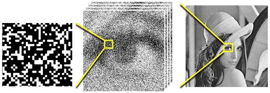
2. Creating Images from Jots
3. Imaging Characteristics
3.1. Hurter-Driffield Characteristic Response (D-LogH)
3.2. Flux Capacity
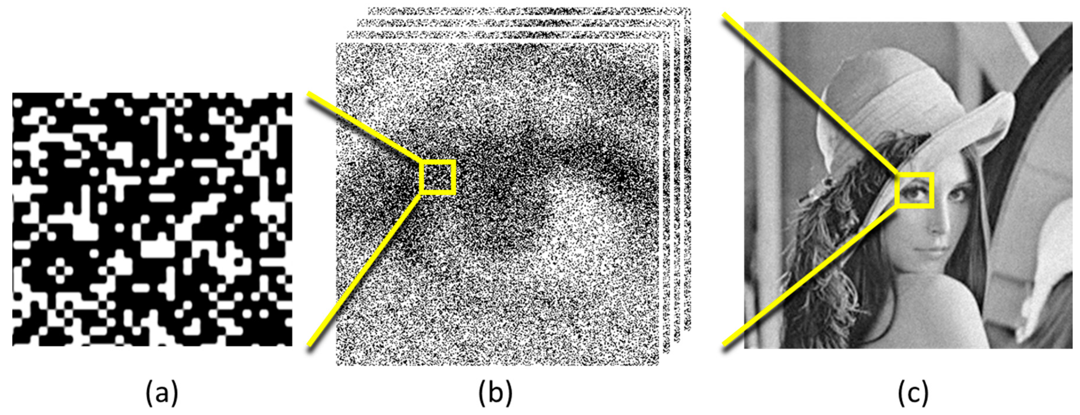
3.3. Multi-Bit QIS
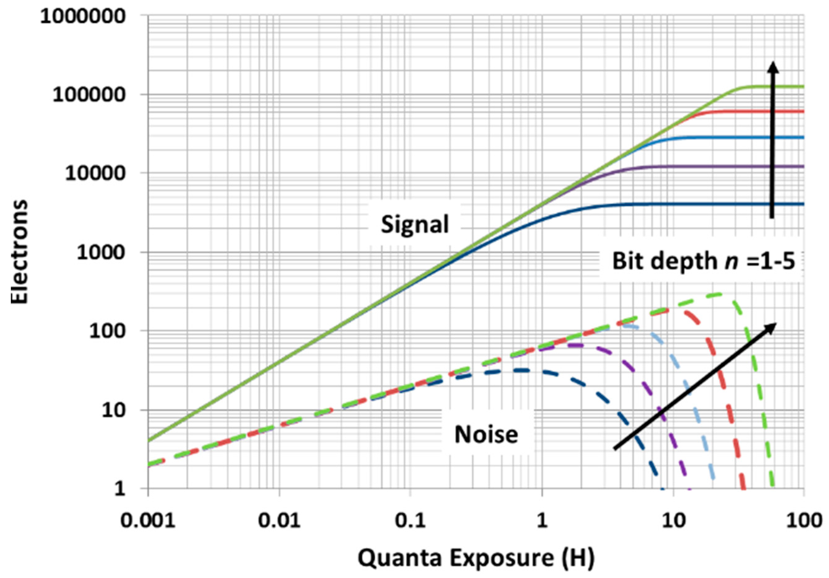
3.4. Signal-to-Noise Ratio (SNR) and Dynamic Range (DR)
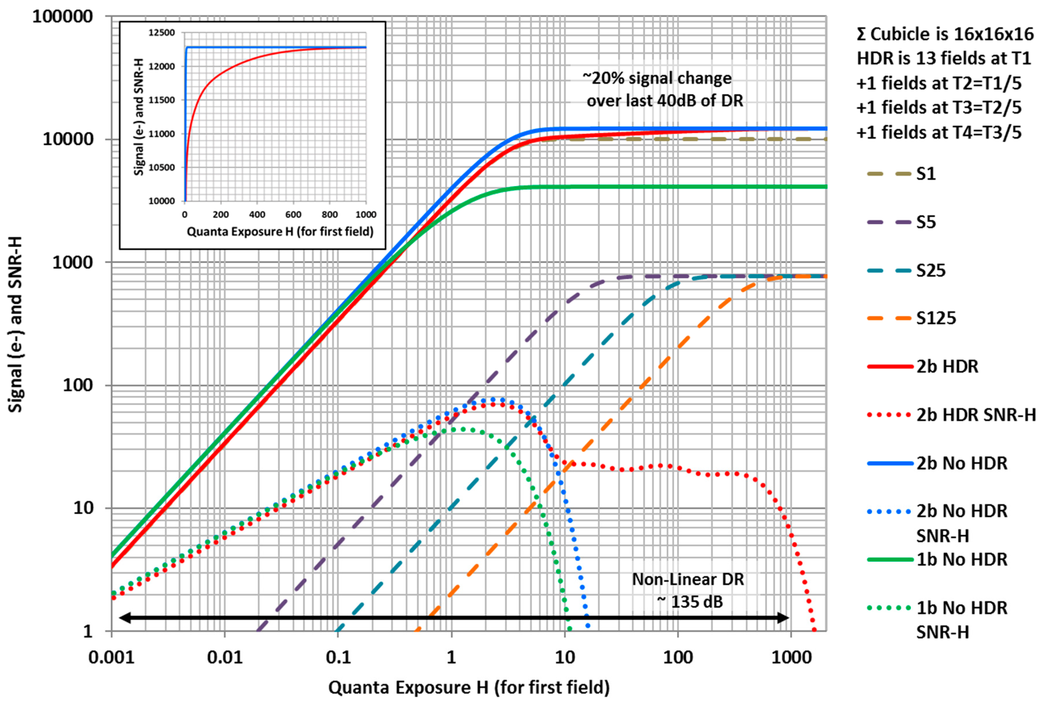
3.5. High Dynamic Range (HDR)
4. Read Noise and Counting Error Rates
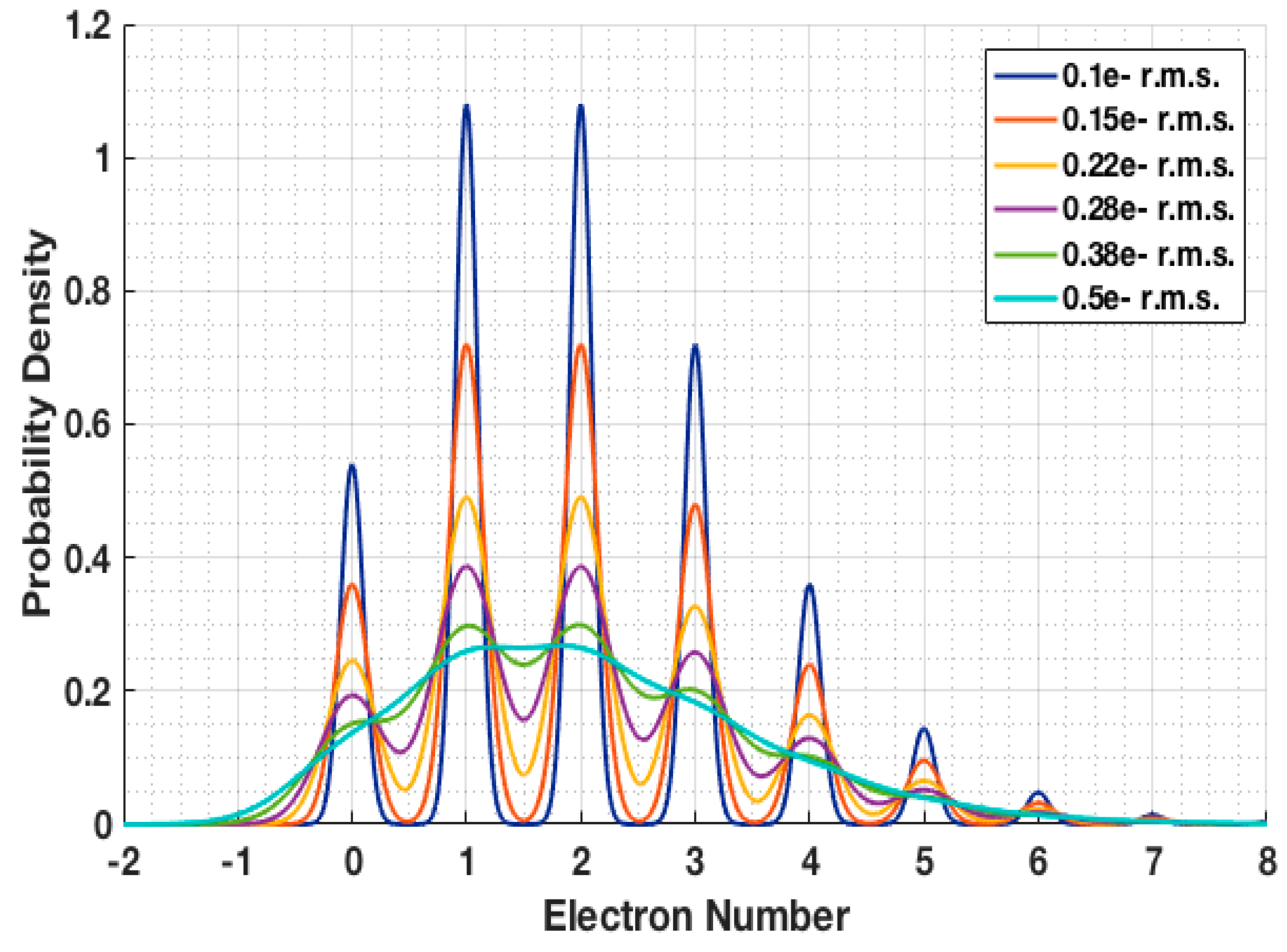
4.1. Read Noise and Readout Signal Probability
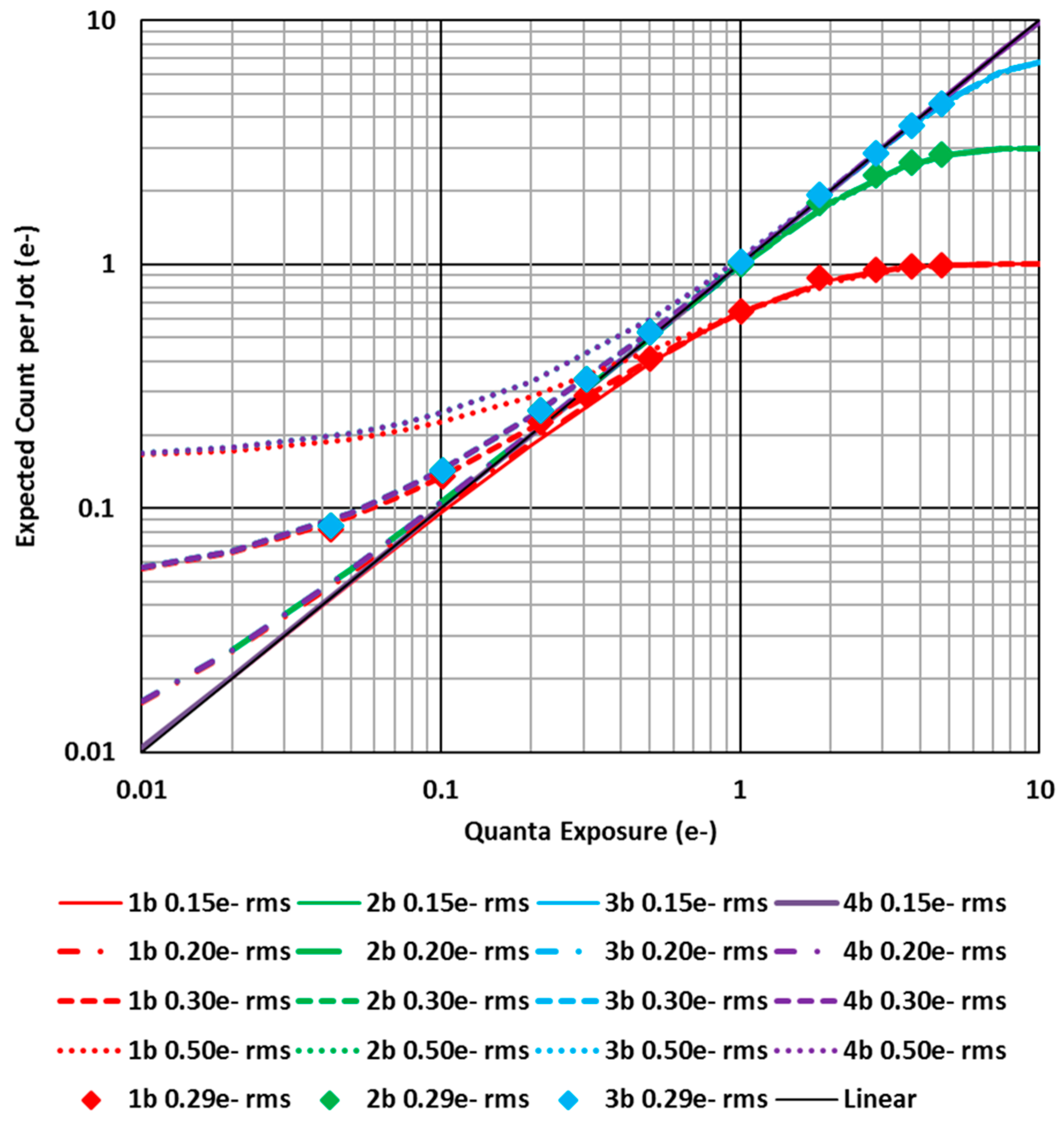
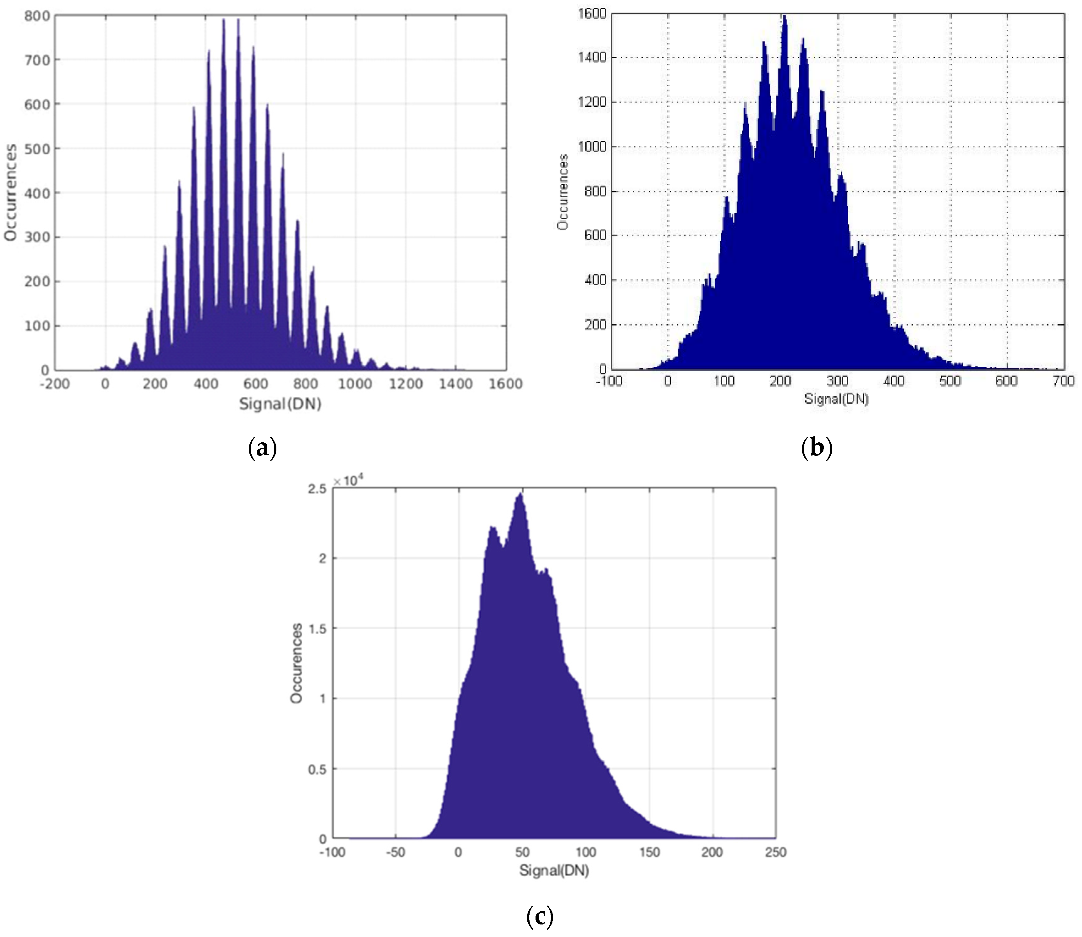
4.2. Quantization and Bin Counts
5. Jot Device
5.1. Background and Motivation
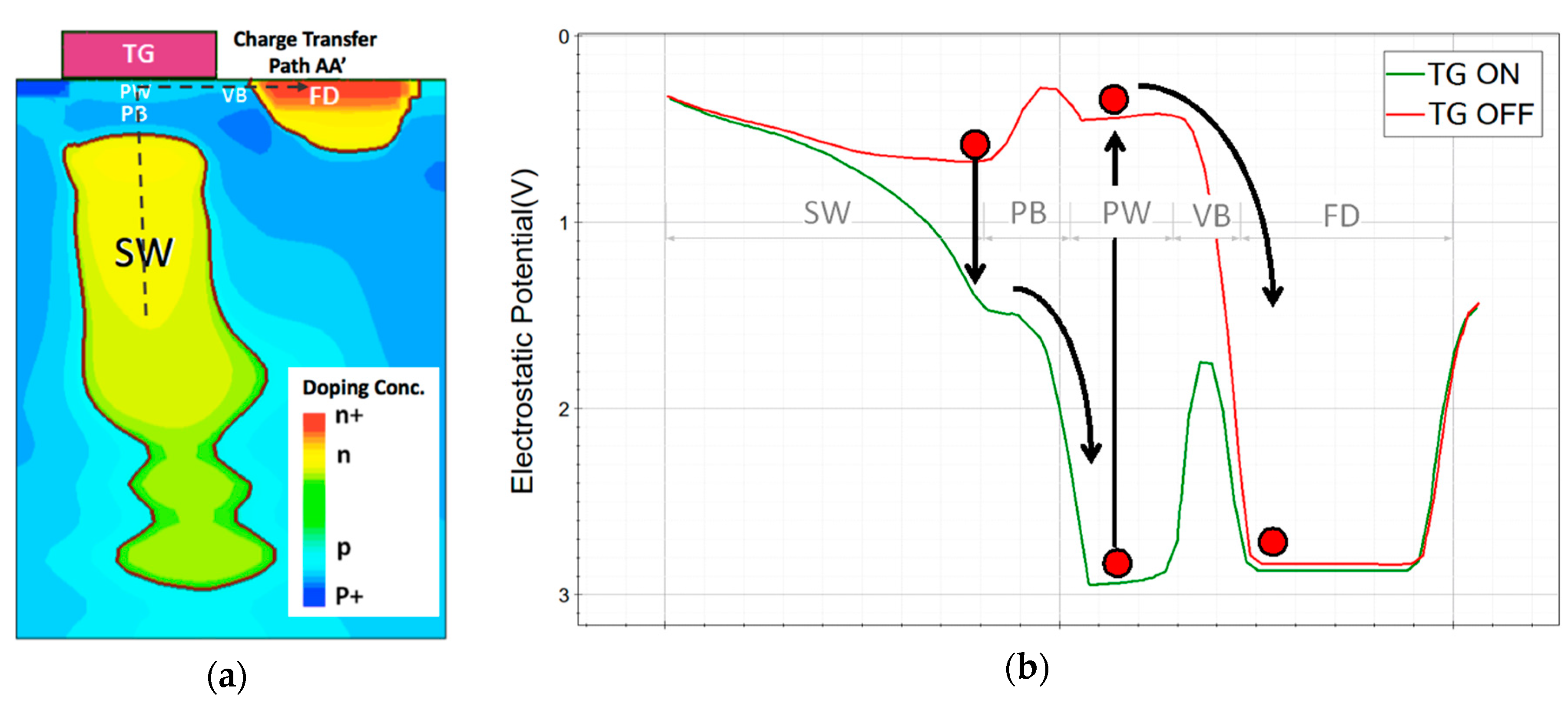
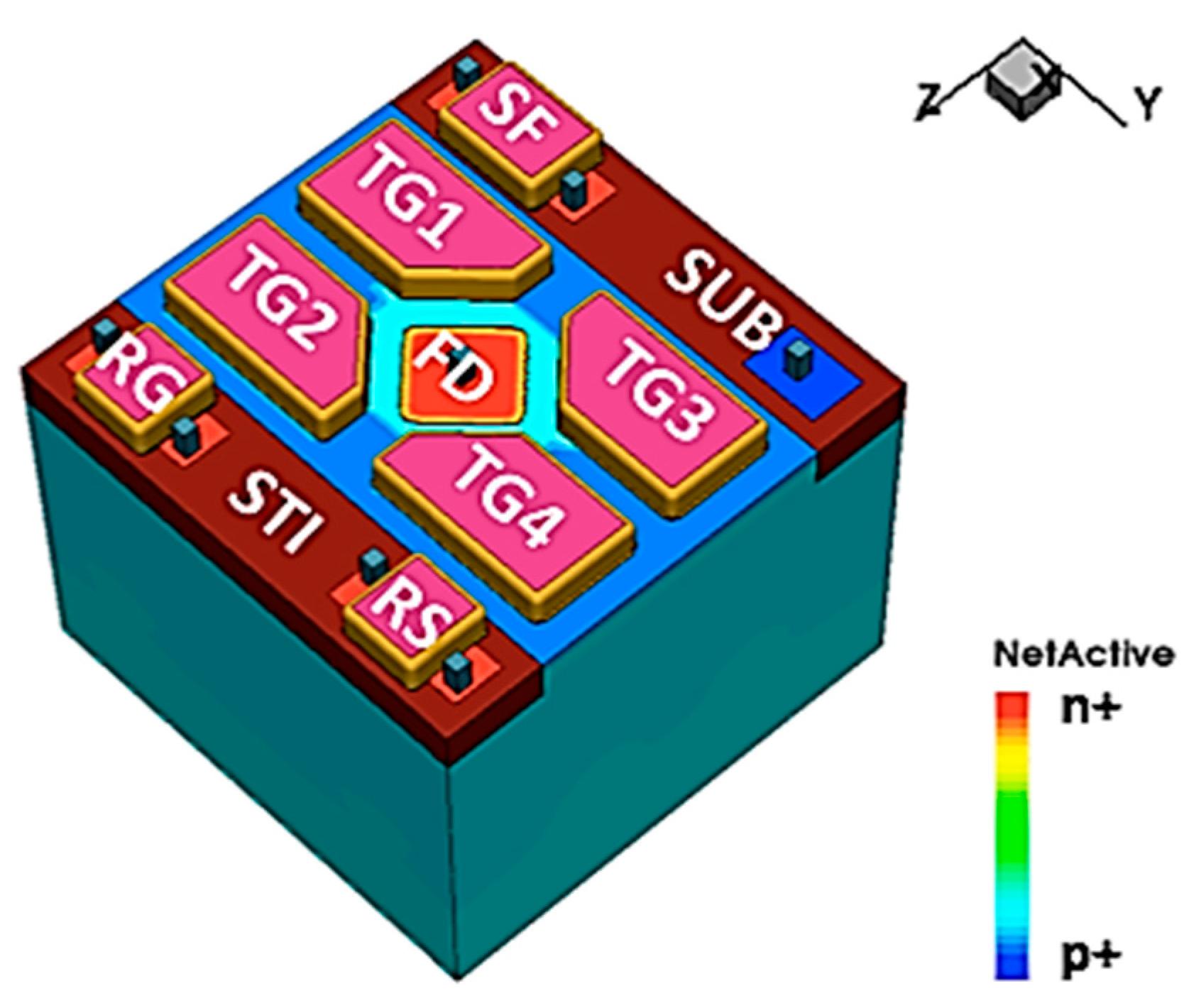
5.2. High CG Pump-Gate Jot Devices
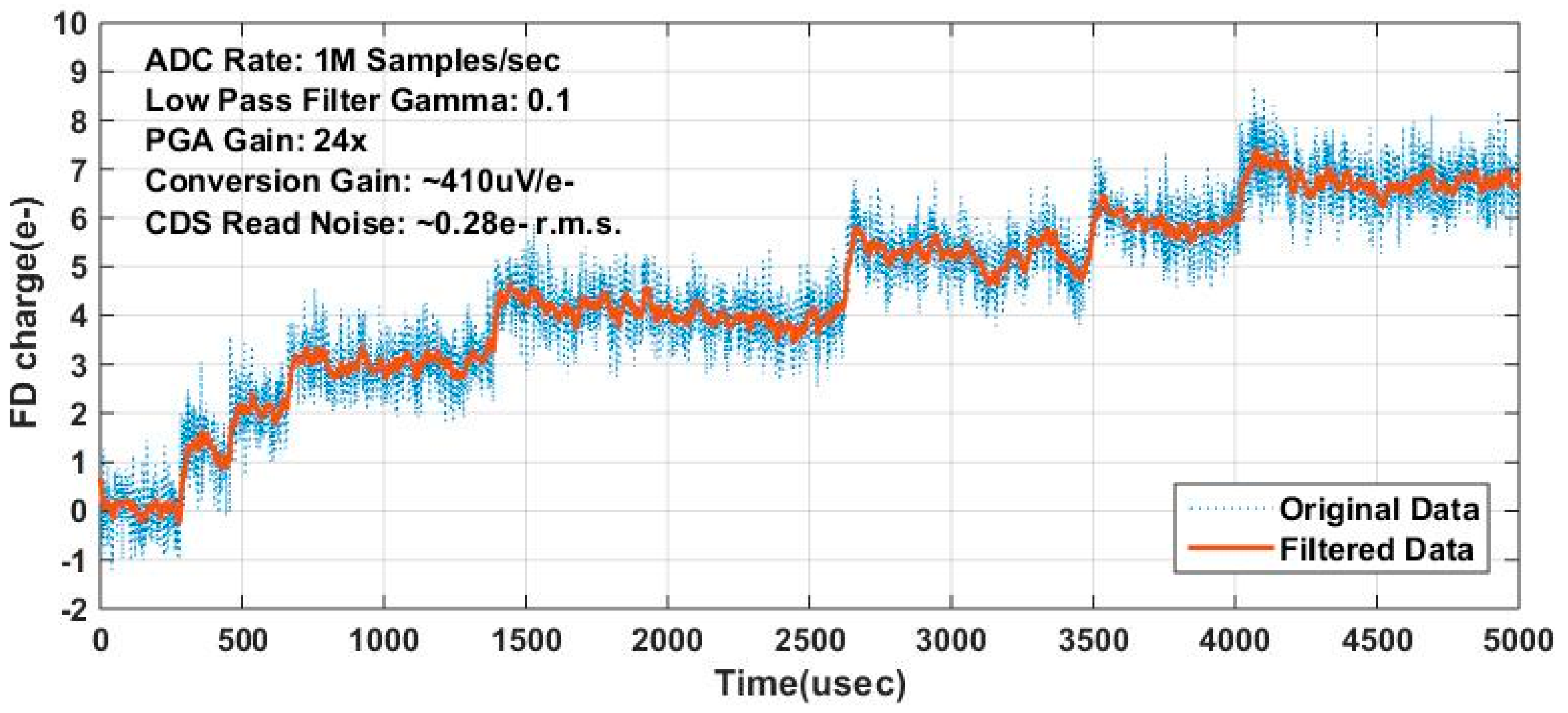
5.3. Photoelectron Counting Capability
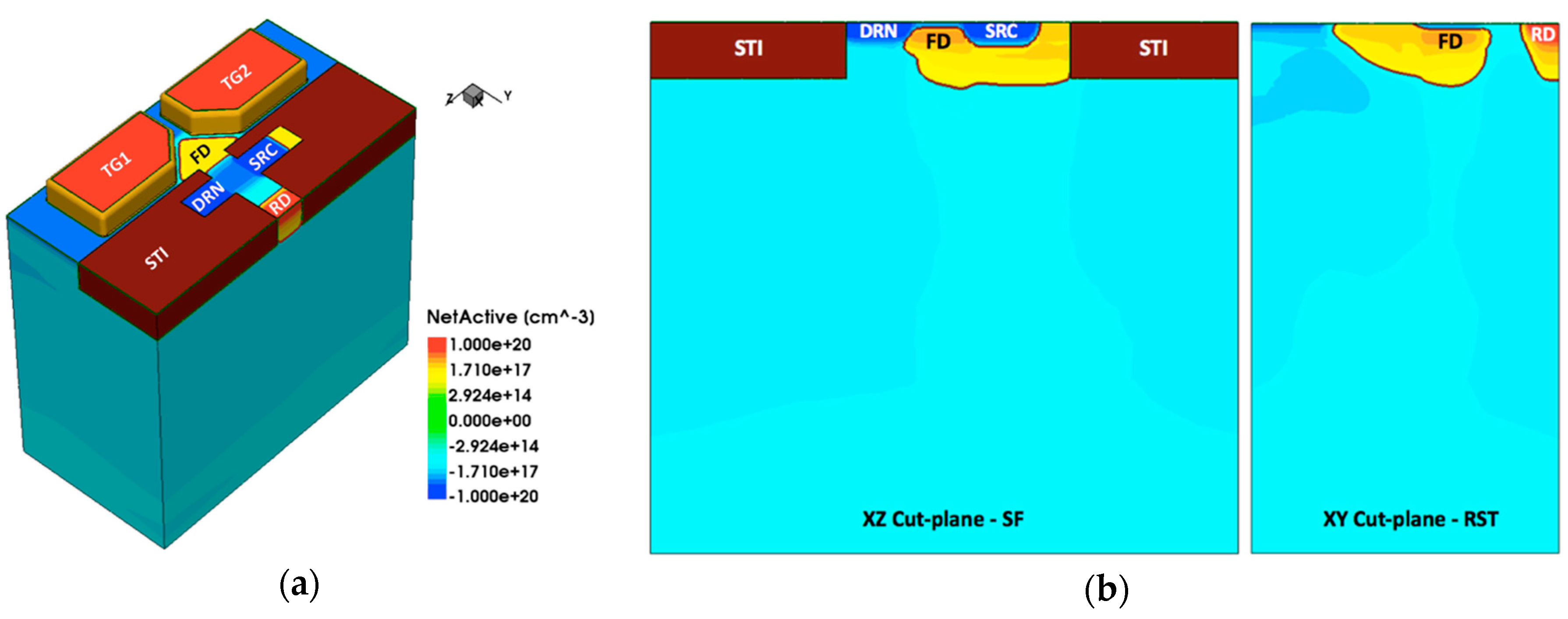
5.4. Jot Device with JFET SF
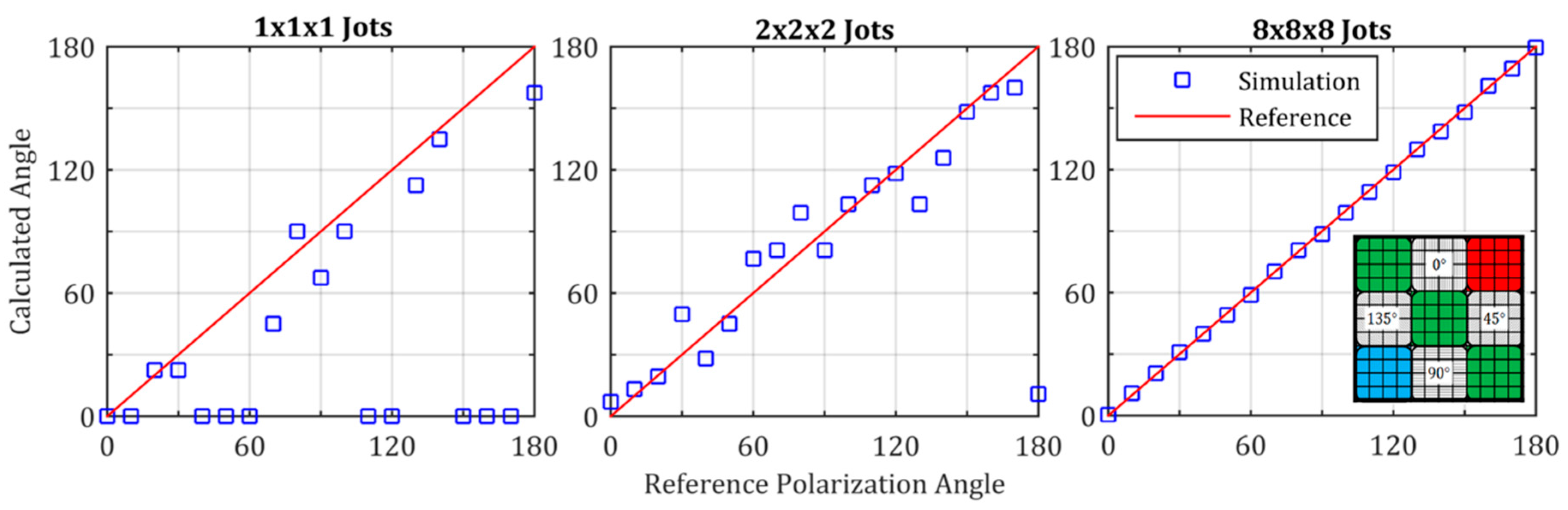
5.5. Color and Polarization Filters
6. Low-Power and High-Speed Readout Circuits
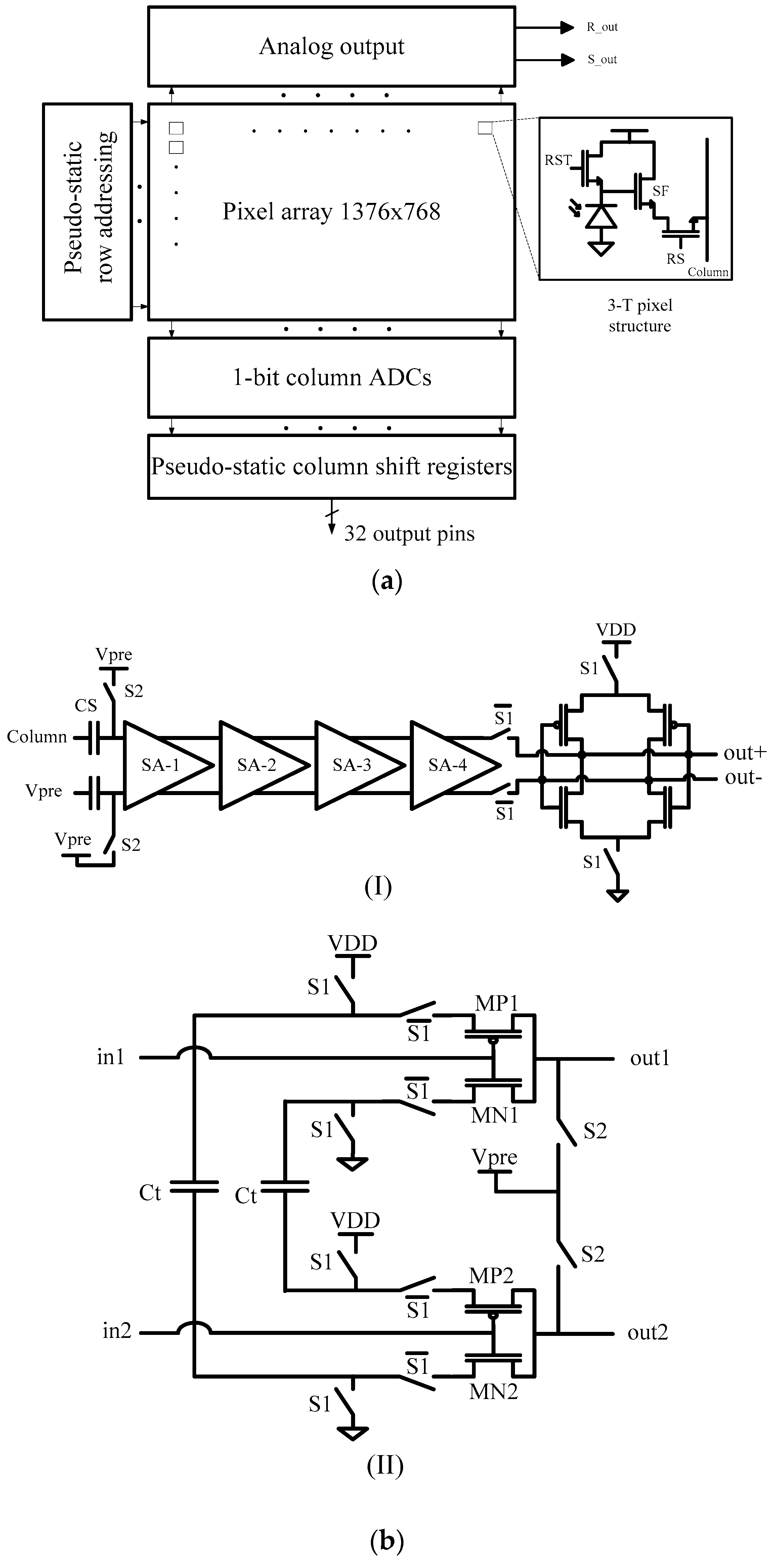
6.1. Readout Circuits for Single-Bit QIS
6.2. Readout Circuits for Multi-Bit QIS
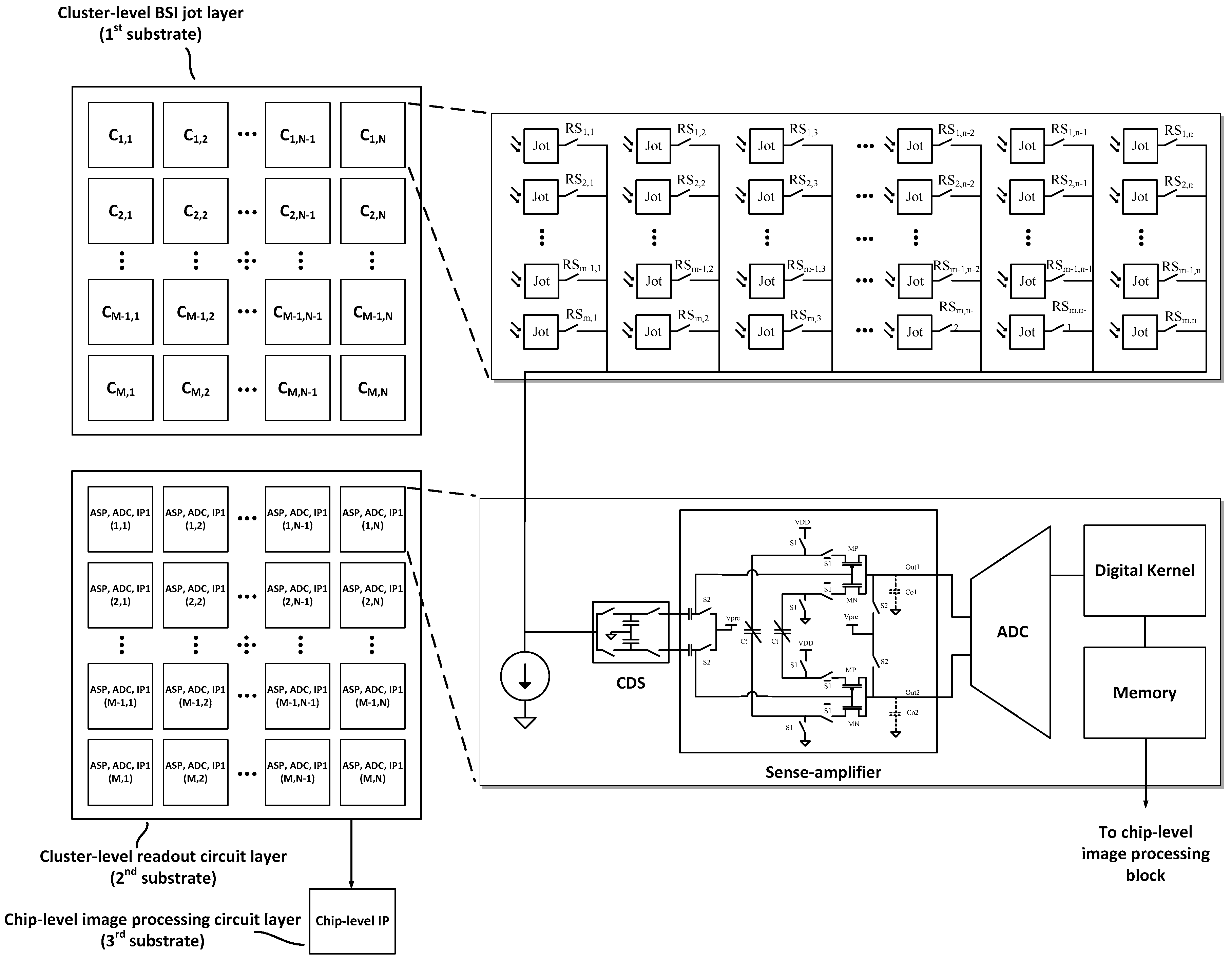
6.3. Stacked QIS
7. Conclusions
Acknowledgments
Conflicts of Interest
Abbreviations
| ADC | analog to digital converter |
| BSI | backside illumination |
| CCD | charge-coupled device |
| CDS | correlated double sampling |
| CFA | color filter array |
| CG | conversion gain |
| CIS | CMOS image sensor |
| CMOS | complementary metal oxide semiconductor |
| CMS | correlated multiple sampling |
| CTA | charge transfer amplifier |
| DR | dynamic range |
| DRN | drain |
| DSERN | deep sub-electron read noise |
| EMCCD | electron-multiplying CCD |
| EPFL | École Polytechnique Fédérale de Lausanne |
| FD | floating diffusion |
| FOM | figure of merit |
| FWC | full-well capacity |
| HDR | high dynamic range |
| I/O | input-output |
| JFET | junction field effect transistor |
| MOSFET | metal oxide semiconductor field effect transistor |
| MTF | modulation transfer function |
| PCH | photon-counting histogram |
| PG | pump gate |
| PW | p-type well |
| QE | quantum efficiency |
| QIS | quanta image sensor |
| RG | reset gate |
| r.m.s. | root-mean-square |
| RT | room temperature |
| RTS | random telegraph signal |
| SDL | sub-diffraction limit |
| SEFET | single-electron field effect transistor |
| SF | source-follower |
| SNR | signal to noise ratio |
| SNR-H | exposure-referred SNR |
| SPAD | single photon avalanche detector |
| SRC | source |
| STI | shallow trench isolation |
| SW | storage well |
| TCAD | technology computer-aided design |
| TDI | time delay integration |
| TG | transfer gate |
| TPG | tapered reset-gate pump gate |
| VPM | valley peak modulation |
References
- Fossum, E.R. Image Sensor Using Single Photon Jots and Processor to Create Pixels. U.S. Patent 8,648,287, 11 February 2014. [Google Scholar]
- Fossum, E.R. Some Thoughts on Future Digital Still Cameras. In Image Sensors and Signal Processing for Digital Still Cameras; Nakamura, J., Ed.; CRC Press: Boca Raton, FL, USA, 2005; pp. 305–314. [Google Scholar]
- Fossum, E.R. What to do with sub-diffraction-limit (SDL) pixels?—A proposal for a gigapixel digital film sensor (DFS). In Proceedings of the 2005 IEEE Workshop on Charge-Coupled Devices and Advanced Image Sensors, Karuizawa, Japan, 9–11 June 2005.
- Fossum, E.R. Gigapixel Digital Film Sensor. In Nanospace Manipulation of Photons and Electrons for Nanovision Systems, Proceedings of the 7th Takayanagi Kenjiro Memorial Symposium and the 2nd International Symposium on Nanovision Science, University of Shizuoka, Hamamatsu, Japan, 25–26 October 2005.
- Fossum, E.R.; Cha, D.-K.; Jin, Y.-G.; Park, Y.-D.; Hwang, S.-J. High Sensitivity Image Sensors Including a Single Electron Field Effect Transistor and Methods of Operating the Same. U.S. Patent 8,546,901, 1 October 2013. U.S. Patent 8,803,273, 12 August 2014. [Google Scholar]
- Fossum, E. The Quanta Image Sensor (QIS): Concepts and Challenges. In Proceedings of the 2011 OSA Topical Mtg on Computational Optical Sensing and Imaging, Toronto, ON, Canada, 10–14 July 2011.
- Chen, S.; Ceballos, A.; Fossum, E.R. Digital integration sensor. In Proceedings of the 2013 International Image Sensor Workshop, Snowbird, UT, USA, 12–16 June 2013.
- Hondongwa, D.; Ma, J.; Masoodian, S.; Song, Y.; Odame, K.; Fossum, E.R. Quanta Image Sensor (QIS): Early Research Progress. In Applied Industrial Optics: Spectroscopy, Imaging and Metrology, Proceedings of the 2013 Optical Social America Topical Meeting on Imaging Systems, Arlington, VA, USA, 24–27 June 2013.
- Fossum, E.R. Modeling the performance of single-bit and multi-bit quanta image sensors. IEEE J. Electron Devices Soc. 2013, 1, 166–174. [Google Scholar] [CrossRef]
- Masoodian, S.; Odame, K.; Fossum, E.R. Low-power readout circuit for quanta image sensors. Electron. Lett. 2014, 50, 589–591. [Google Scholar] [CrossRef]
- Ma, J.; Hondongwa, D.; Fossum, E.R. Jot devices and the quanta image sensor. In Proceedings of the 2014 IEEE International Electron Devices Meeting (IEDM) on Technical Digest, San Francisco, CA, USA, 15–17 December 2014; pp. 247–250.
- Anzagira, L.; Fossum, E.R. Color filter array patterns for small-pixel image sensors with substantial cross talk. J. Opt. Soc. Am. A 2015, 32, 28–34. [Google Scholar] [CrossRef] [PubMed]
- Ma, J.; Fossum, E.R. A pump-gate jot device with high conversion gain for quanta image sensors. IEEE J. Electron Devices Soc. 2015, 3, 73–77. [Google Scholar] [CrossRef]
- Fossum, E.R. Multi-bit Quanta Image Sensors. In Proceedings of the 2015 International Image Sensor Workshop (IISW), Vaals, The Netherlands, 8–11 June 2015.
- Masoodian, S.; Rao, A.; Ma, J.; Odame, K.; Fossum, E.R. A 2.5 pJ Readout Circuit for 1000 fps Single-Bit Quanta Image Sensors. In Proceedings of the 2015 International Image Sensor Workshop (IISW), Vaals, The Netherlands, 8–11 June 2015.
- Zizza, R. Jots to Pixels: Image Formation Options for the Quanta Image Sensor. M.S. Thesis, Thayer School of Engineering at Dartmouth College, Hanover, NH, USA, July 2015. [Google Scholar]
- Ma, J.; Fossum, E.R. Quanta image sensor jot with sub 0.3 e− r.m.s. read noise and photon counting capability. IEEE Electron Device Lett. 2015, 36, 926–928. [Google Scholar] [CrossRef]
- Ma, J.; Starkey, D.; Rao, A.; Odame, K.; Fossum, E.R. Characterization of Quanta image sensor pump-gate jots with deep sub-electron read noise. IEEE J. Electron Devices Soc. 2015, 3, 472–480. [Google Scholar] [CrossRef]
- Masoodian, S.; Rao, A.; Ma, J.; Odame, K.; Fossum, E.R. A 2.5 pJ/b binary image sensor as a pathfinder for Quanta image sensors. IEEE Trans. Electron Devices 2016, 63, 100–105. [Google Scholar] [CrossRef]
- Ma, J.; Anzagira, L.; Fossum, E.R. A 1 µm-pitch quanta image sensor jot device with shared readout. IEEE J. Electron Devices Soc. 2016, 4, 83–89. [Google Scholar] [CrossRef]
- Fossum, E.R. Photon counting error rates in single-bit and multi-bit quanta image sensors. IEEE J. Electron Devices Soc. 2016, 4, 136–143. [Google Scholar] [CrossRef]
- Starkey, D.A.; Fossum, E.R. Determining conversion gain and read noise using a photon-counting histogram method for deep sub-electron read noise image sensors. IEEE J. Electron Devices Soc. 2016, 4, 129–135. [Google Scholar] [CrossRef]
- Fossum, E.R. Photon counting without avalanche multiplication-progress on the quanta image sensor. In Proceedings of the Image Sensors 2016 Europe, London, UK, 15–17 March 2016.
- Anzagira, L.; Fossum, E.R. Application of the quanta image sensor concept to linear polarization imaging—A theoretical study. J. Opt. Soc. Am. A 2016, 33, 1147–1154. [Google Scholar] [CrossRef] [PubMed]
- Masoodian, S.; Fossum, E.R. A 32 × 12,000, 1040 fp/s binary image sensor with 0.4 pJ/b readout circuits fabricated in 65 nm backside-illuminated CIS process as a path-finder for 1 Gpixel 1040 fps binary image sensor. to be published.
- Ma, J.; Fossum, E.R. TCAD simulation of a quanta image sensor jot device with a JFET source follower. to be published.
- Dutton, N.A.W.; Parmesan, L.; Holmes, A.J.; Grant, L.A.; Henderson, R.K. 320 × 240 oversampled digital single photon counting image sensor. In Proceedings of the 2014 IEEE Symposium on VLSI Circuits Digest of Technical Papers, Honolulu, HI, USA, 10–13 June 2014; pp. 1–2.
- Gyongy, I.; Dutton, N.; Parmesan, L.; Davies, A.; Saleeb, R.; Duncan, R.; Rickman, C.; Dalgarno, P.; Henderson, R.K. Bit-plane processing techniques for low-light, high-speed imaging with a SPAD-based QIS. In Proceedings of the 2015 International Image Sensor Workshop (IISW), Vaals, The Netherlands, 8–11 June 2015.
- Dutton, N.A.W.; Parmesan, L.; Gnecchi, S.; Gyongy, I.; Calder, N.; Rae, B.R.; Grant, L.A.; Henderson, R.K. Oversampled ITOF imaging techniques using SPAD-based quanta image sensors. In Proceedings of the 2015 International Image Sensor Workshop (IISW), Vaals, The Netherlands, 8–11 June 2015.
- Dutton, N.A.; Gyongy, I.; Parmesan, L.; Gnecchi, S.; Calder, N.; Rae, B.; Pellegrini, S.; Grant, L.A.; Henderson, R.K. A SPAD-based QVGA image sensor for single-photon counting and quanta imaging. IEEE Trans. Electron Devices 2016, 63, 189–196. [Google Scholar] [CrossRef]
- Niclass, C.; Rochas, A.; Besse, P.-A.; Popovic, R.S.; Charbon, E. CMOS imager based on single photon avalanche diodes. In Proceedings of the 13th International Conference on Solid-State Sensors, Actuators and Microsystems, Digest of Technical Papers (TRANSDUCERS’05), Seoul, Korea, 5–9 June 2015; Volume 1, pp. 1030–1034.
- Charbon, E. Will avalanche photodiode arrays ever reach 1 megapixel? In Proceedings of the 2007 International Image Sensor Workshop (IISW), Ogunquit, ME, USA, 7–10 June 2007.
- Sbaiz, L.; Yang, F.; Charbon, E.; Süsstrunk, S.; Vetterli, M. The gigavision camera. In Proceedings of the 2009 IEEE International Conference on Acoustics, Speech and Signal (ICASSP 2009), Taipei, Taiwan, 19–24 April 2009.
- Yang, F.; Sbaiz, L.; Charbon, E.; Süsstrunk, S.; Vetterli, M. On pixel detection threshold in the gigavision camera. Proc. SPIE 2010, 7537. [Google Scholar] [CrossRef]
- Yoon, H.J.; Charbon, E. The Gigavision Camera: A 2 Mpixel Image Sensor with 0.56 μm2 1-T digital pixels. In Proceedings of the 2011 International Image Sensor Workshop (IISW), Hokkaido, Japan, 8–11 June 2011.
- Yang, F.; Lu, Y.M.; Sbaiz, L.; Vetterli, M. Bits from photons: oversampled image acquisition using binary Poisson statistics. IEEE Trans. Image Process. 2012, 21, 1421–1436. [Google Scholar] [CrossRef] [PubMed]
- Hurter, F.; Driffield, V.C. Photo-Chemical Investigations and a New Method of Determination of the Sensitiveness of Photographic Plates—Reprinted from The Journal of the Society of Chemical Industry, 31st May 1890. No. 5, Vol IX. The Photographic Researches of Ferdinand Hurter and Vero C; Driffield, W.B., Ed.; The Royal Photographic Society of Great Britain: London, UK, 1920; pp. 76–122. Available online: https://archive.org/details/memorialvolumeco00hurtiala (accessed on 8 August 2016).
- Oliver, C.J.; Pike, E.R. Measurement of low light flux by photon counting. J. Phys. D Appl. Phys. 1968, 1, 1459. [Google Scholar] [CrossRef]
- Nieto, J. New Aspects of Galaxy Photometry. In Proceedings of the Specialized Meeting, Toulouse, France, 17–21 September 1984; Springer-Verlag: Heidlberg, Germany, 1985; Volume 232. [Google Scholar]
- Nieto, J.; Thouvenot, E. Recentring and selection of short-exposure images with photon-counting detectors. I-Reliability tests. Astron. Astrophys. 1991, 241, 663–672. [Google Scholar]
- Bondarenko, G.; Dolgoshein, B.; Golovin, V.; Ilyin, A.; Klanner, R.; Popova, E. Limited Geiger-mode silicon photodiode with very high gain. Nucl. Phys. B Proc. Suppl. 1998, 61, 347–352. [Google Scholar] [CrossRef]
- Dierickx, B. Electronic image sensors vs. film: Beyond state of the art. In Proceedings of the OEEPE Workshop on Automation in Digital Photogrammetric Production, Paris, France, 21–24 June 1999.
- Mackay, C.D.; Tubbs, R.N.; Bell, R.; Burt, D.J.; Jerram, P.; Moody, I. Sub-electron read noise at MHz pixel rates. Proc. SPIE 2011, 4306, 289–298. [Google Scholar]
- Wolfel, S.; Herrmann, S.; Lechner, P.; Lutz, G.; Porro, M.; Richter, R.; Struder, L.; Treis, J. Sub-electron noise measurements on RNDR Devices. In Proceedings of the IEEE Nuclear Science Symposium Conference Record, San Diego, CA, USA, 29 October–1 November 2006; pp. 63–69.
- Lotto, C.; Seitz, P.; Baechler, T. A sub-electron readout noise CMOS image sensor with pixel-level open-loop voltage amplification. In Proceedings of the IEEE International Solid-State Circuits Conference (ISSCC), San Francisco, CA, USA, 20–24 February 2012.
- Chen, Y.; Xu, Y.; Chae, Y.; Mierop, A. A 0.7 e− r.m.s.-temporal-readout-noise CMOS image sensor for low-light-level imaging. In Proceedings of the IEEE International Solid-State Circuits Conference (ISSCC), San Francisco, CA, USA, 20–24 February 2012.
- Yao, Q.; Dierickx, B.; Dupont, B. CMOS image sensor reaching 0.34 e− r.m.s. read noise by inversion-accumulation cycling. In Proceedings of the 2015 International Image Sensor Workshop (IISW), Vaals, The Netherlands, 8–11 June 2015.
- Boukhayma, A.; Peizerat, A.; Enz, C. A 0.4 e− r.m.s. Temporal Readout Noise, 7.5 μm pitch and a 66% fill factor pixel for low light CMOS image sensors. In Proceedings of the 2015 International Image Sensor Workshop (IISW), Vaals, The Netherlands, 8–11 June 2015.
- Parks, C.; Kosman, S.; Nelson, E.; Roberts, N.; Yaniga, S. A 30 fps 1920 × 1080 pixel electron multiplying CCD image sensor with per-pixel switchable gain. In Proceedings of the 2015 International Image Sensor Workshop (IISW), Vaals, The Netherlands, 8–11 June 2015.
- Janesick, J.; Elliott, T.; Andrews, J.; Tower, J. Fundamental performance differences of CMOS and CCD imagers: Part VI. Proc. SPIE 2015, 9591. [Google Scholar] [CrossRef]
- Seo, M.-W.; Kawahito, S.; Kagawa, K.; Yasutomi, K. A 0.27 e- r.m.s. read noise 220-μV/e- conversion gain reset-gate-less CMOS image sensor with 0.11-μm CIS process. IEEE Electron Device Lett. 2015, 36, 1344–1347. [Google Scholar]
- Berezin, V. Active Pixel Sensor with Mixed Analog and Digital Signal integration. U.S. Patent 7,139,025, 21 November 2006. [Google Scholar]
- Chan, S.H.; Lu, Y.M. Efficient image reconstruction for gigapixel quantum image sensors. In Proceedings of the 2014 IEEE Global Conference on Signal and Information Processing (GlobalSIP), Atlanta, GA, USA, 3–5 December 2014; pp. 312–316.
- Misc. Private Communications, 2005–2016.
- Yadid-Pecht, O.; Staller, C.; Fossum, E.R. Wide intrascene dynamic range CMOS APS using dual sampling. IEEE Trans. Electron Devices 1997, 44, 1721–1723. [Google Scholar] [CrossRef]
- Teranishi, N. Required conditions for photon-counting image sensors. IEEE Trans. Electron Devices 2012, 59, 2199–2205. [Google Scholar] [CrossRef]
- Boukhayma, A.; Peizerat, A.; Enz, C. Noise reduction techniques and scaling effects towards photon counting CMOS image sensors. Sensors 2016, 16, 514. [Google Scholar] [CrossRef]
- Kwon, S.; Kwon, H.; Choi, W.; Song, H.-S.; Lee, H. Effects of shallow trench isolation on low frequency noise characteristics of source-follower transistors in CMOS image sensors. Solid State Electron. 2016, 119, 29–32. [Google Scholar] [CrossRef]
- Black, R.D.; Weissman, M.B.; Restle, P.J. 1/f noise in silicon wafers. J. Appl. Phys. 1982, 53, 6280. [Google Scholar] [CrossRef]
- Norton, P.W. On the Origin of 1/f Noise in Electronic Devices. Unpublished White Paper. 2011. [Google Scholar]
- Suh, S.; Itoh, S.; Aoyama, S.; Kawahito, S. Column-parallel correlated multiple sampling circuits for CMOS image sensors and their noise reduction effects. Sensors 2010, 10, 9139–9154. [Google Scholar] [CrossRef] [PubMed]
- Kusuhara, F.; Wakashima, S.; Nasuno, S.; Kuroda, R.; Sugawa, S. Analysis and reduction of floating diffusion capacitance components of CMOS image sensor for photon-countable sensitivity. In Proceedings of the 2015 International Image Sensor Workshop (IISW), Vaals, The Netherlands, 8–11 June 2015.
- Guidash, M. Active Pixel Sensor with Punch-Through Reset and Cross-Talk Suppression. U.S. Patent 5,872,371, 16 February 1999. [Google Scholar]
- Koskinen, S.; Kalevo, O.; Rissa, R.; Alakarhu, J. Color Filters for Sub-Diffraction Limit-Sized Light Sensors. U.S. Patent 8,134,115, 13 March 2012. [Google Scholar]


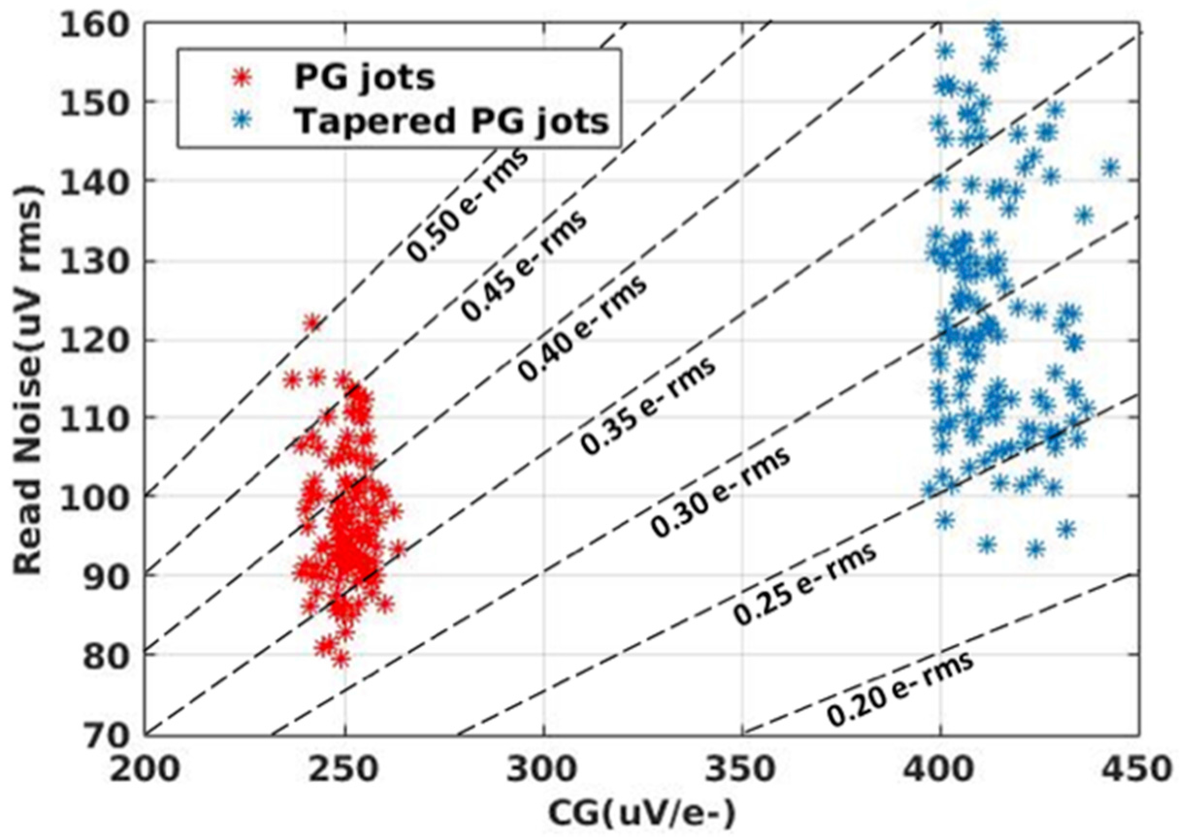
| Quantity | TPG Jot | Non-Shared PG Jot | Shared PG Jot |
|---|---|---|---|
| CG | 410 μV/e− | 250 μV/e− | 230 μV/e− |
| Read Noise | 0.29 e− r.m.s. (129 μV r.m.s.) | 0.38 e− r.m.s. (95.3 μV r.m.s.) | 0.48 e− r.m.s. (110 μV r.m.s.) |
| SF Size | 0.2 × 0.2 μm2 | 0.2 × 0.4 μm2 | 0.2 × 0.4 μm2 |
| Dark Current @ RT | 0.09 e−/s (0.73 pA/cm2) | 0.12 e−/s (0.98 pA/cm2) | Not measured |
| Dark Current @ 60 °C | 1.29 e−/s (10.5 pA/cm2) | 1.26 e−/s (10.2 pA/cm2) | 0.71 e−/s (11.4 pA/cm2) |
| Lag @ RT | <0.1 e− | <0.1 e− | <0.12 e− |
| Process | X-FAB, 0.18 µm, 6M1P (Non-Standard Implants) | |
|---|---|---|
| VDD | 1.3 V (Analog and Digital), 1.8 V (Array), 3 V (I/O pads) | |
| Pixel type | 3T-APS | |
| Pixel pitch | 3.6 µm | |
| Photo-detector | Partially pinned photodiode | |
| Conversion gain | 119 µV/e− | |
| Array | 1376 (H) × 768 (V) | |
| Column noise | 2 e− | |
| Field rate | 1000 fps | |
| ADC sampling rate | 768 KSa/s | |
| ADC resolution | 1 bit (VLSB = 1 mV) | |
| Output data rate | 32 (output pins) × 33 Mb/s = 1 Gb/s | |
| Package | PGA with 256 pins | |
| Power | Pixel array | 8.6 mW |
| ADCs | 2.6 mW | |
| Addressing | 3.8 mW | |
| I/O pads | 5 mW | |
| Total | 20 mW | |
© 2016 by the authors; licensee MDPI, Basel, Switzerland. This article is an open access article distributed under the terms and conditions of the Creative Commons Attribution (CC-BY) license (http://creativecommons.org/licenses/by/4.0/).
Share and Cite
Fossum, E.R.; Ma, J.; Masoodian, S.; Anzagira, L.; Zizza, R. The Quanta Image Sensor: Every Photon Counts. Sensors 2016, 16, 1260. https://doi.org/10.3390/s16081260
Fossum ER, Ma J, Masoodian S, Anzagira L, Zizza R. The Quanta Image Sensor: Every Photon Counts. Sensors. 2016; 16(8):1260. https://doi.org/10.3390/s16081260
Chicago/Turabian StyleFossum, Eric R., Jiaju Ma, Saleh Masoodian, Leo Anzagira, and Rachel Zizza. 2016. "The Quanta Image Sensor: Every Photon Counts" Sensors 16, no. 8: 1260. https://doi.org/10.3390/s16081260