Analysis and Simulation of the Optical Properties of a Quantum Dot on a Graphene Nanoribbon System


1
Photonics and Nanocrystal Research Laboratory (PNRL), Faculty of Electrical and Computer Engineering, University of Tabriz, Tabriz 5166614761, Iran
2
Department of Mechanical, Electronics and Chemical Engineering, OsloMet—Oslo Metropolitan University, 0167 Oslo, Norway
*
Author to whom correspondence should be addressed.
Photonics 2022, 9(4), 220; https://doi.org/10.3390/photonics9040220
Submission received: 14 January 2022
/
Revised: 26 February 2022
/
Accepted: 1 March 2022
/
Published: 27 March 2022
(This article belongs to the Topic Optical and Optoelectronic Materials and Applications)
Abstract
:In this work, we theoretically study the optical properties of a graphene nanoribbon with a quantum dot (QD) on it. The system consists of a graphene nanoribbon with dimensions of 400 × 3100 (nm2) and a quantum dot with a nanoscale radius. The quantum dot is symmetrically located at the center of the graphene nanoribbon to simplify the mathematical model. To calculate the optical properties (susceptibility) of the system, a broadband electromagnetic wave (0.5–2.5 μm) is applied to the structure to model dipole-dipole interaction. Considering the input field and calculating the total induced polarization, the optical susceptibility of the system is calculated. The applied electromagnetic field excites the surface plasmon on the graphene nanoribbon and the excitons of QDs. The induced dipoles in the graphene nanoribbon and the QD will interact with each other. We show that the parameters of both materials strongly influence dipole-dipole interaction. In particular, the effect of QDs (location on graphene and radius) on the optical properties of the considered system was studied. The obtained results can be used to introduce periodic optical structures in nanoscale by inserting QDs in a periodic array on graphene nanoribbon. Additionally, applications such as reflectors, couplers, and wavelength filters can be designed. Considering the presented theoretical framework, we can describe all the optoelectronic and optomechanical applications of complex nanoscale graphene and QD systems.
1. Introduction
The interaction of light with nanostructures has unique properties that can be used in discrete optical devices in or integrated at the nanometer scale [1]. The number of hybrid systems using nanostructures is very large, and thus this area is of great interest for both research and industry [2]. In this paper, we study the basic theory of surface plasmons in a system comprising a graphene nanoribbon with a QD placed on it using modeling based on the interaction of that polarization with the exciton created in the semiconductor quantum dot. The principle of this study is the interaction between the exciton in the semiconductor quantum dot and the polarization of the surface plasmons formed at the metal-insulator boundary [3]. Extensive fields of applications can be addressed by controlling the effects of these interactions at the nanometer scale [4].
Surface plasmons are created by applying electromagnetic waves to the surface of a graphene nanoribbon. The induced plasmons on the graphene nanoribbon excite the exciton in the quantum dot, displacing the electron distribution in the QDs; thus inducing a dipole in the quantum dot. Therefore, the electric field generates dipoles in the graphene nanoribbon and quantum dot. The electric field created by the quantum dot on the graphene nanoribbon is due to the polarization of the QD induced by the surface plasmons on the graphene. The numerical simulations show that a periodic optical structure is obtained by placing quantum dots on a graphene nanoribbon in a periodic array. This idea could lead to several interesting applications in classical and quantum optical integrated circuits [5,6]. The massive oscillations of electrons cause surface plasmon polarization in graphene nanoribbons in the conduction band due to the dielectric difference between the graphene and the surroundings media. Plasmonics have been studied extensively due to their applications in optical sensors [7,8], optical switches [9], nano tracks [10], and quantum information processing [11,12]. Noble metals are the best materials in existence for studying surface plasmon polaritons [13]. However, noble metals are difficult to adjust, and exhibit high ohmic losses, limiting their application in optical processing devices [14,15]. Graphene plasmons are an attractive and suitable alternative to noble metal plasmons, because they show plasmon transport over a relatively long distance. In addition, the surface plasmons in graphene have the advantage of being regulated by electrostatic gates [5,9]. Compared to noble metals, graphene has extraordinary optical, electrical, and mechanical properties that originate in part from its zero-mass charge carriers [16]. Graphene is also known as supporting photonic material in emerging optoelectronic applications. Thus, graphene has received much attention in plasmonic research, both theoretically and experimentally [17,18,19].
Recently, experimental research has expanded to the fabrication and study of QD–graphene nanostructures [5,20]. These structures could make a significant contribution to the formation of plasmonic waveguides. Different types of graphene-based waveguides, such as strip structures [21,22], cheek and groove waveguides [23,24], graphene–metal structures [25], and multilayer graphene [26,27,28], have been studied and exploited.
This paper applies electromagnetic theory and the effects of bipolar fields to model dipole–dipole interaction in a graphene–QD system. Using the presented model, the absorption coefficient and surface plasmons of graphene nanoribbon are calculated. The second part of this paper presents an analytical and computational approach for computing the plasmon frequency of graphene. Additionally, the effect of graphene surface plasmons and QDs on the optical properties of the system is investigated. The third section introduces a periodic optical structure with quantum dots on graphene nanoribbon. The proposed combination can be used in classical and quantum optical and mechanical applications.
2. Theoretical Formulation
2.1. Plasma Frequency and Surface Plasmons Polarization of Graphene
Recently, graphene, a one-atom-thick material composed of carbon atoms arranged in a hexagonal lattice, was introduced as a flat (metal-like) plasmonic material. This matter (as an infinitesimally thin, nonlocal two-sided surface) is characterized by a magneto-optically complex conductivity tensor. Under these conditions, the elements of this matrix become independent of microscopic, semi-classical, and quantum mechanical considerations. The combined conductivity of graphene in the absence of magnetic bias is as follows [19].
where , , , KB and T are the radian frequency, the charged particle scattering rate representing the loss mechanism, the chemical potential of the graphene, the Boltzmann constant equal to , and temperature equal to three hundred degrees Kelvin (), respectively. In general, the scattering rate is a function of frequency, temperature, field amplitude, and landau level index. The chemical potential with respect to the density of charged carriers can be controlled by chemical doping or by applying a dc bias voltage. Considering the Maxwell equation , an equivalent complex permittivity for the graphene layer is given as follows:
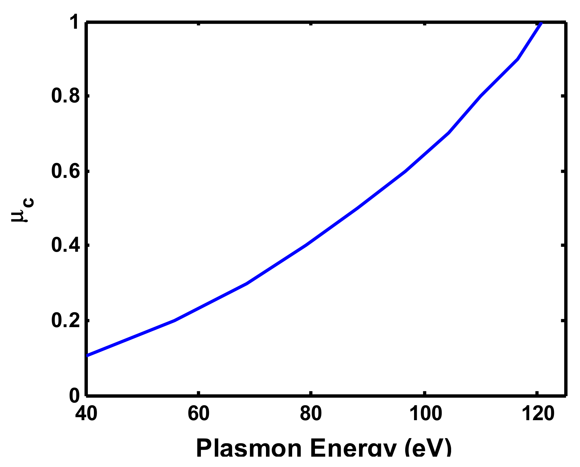
Please note that d is the thickness of the graphene layer. Now the dispersion relation for the proposed structure is derived. In this study, the thickness of the graphene nanoribbon (d) is minimal, and in the numerical simulation step, it is d→0. For the given value of d, the volume conductivity can be defined as described in [9,19]. Based on the free-electron theory and Drude model, the permittivity and conductivity of graphene nanoribbon are frequency-dependent. The most critical parameter in this model is the plasma frequency. At plasma frequency, the real part of the permittivity should be equal to zero. Therefore, the plasmon frequency is a critical factor used in device design. We show that the plasmon frequency changes when modifying the chemical potential of graphene [2,6]. This feature of graphene increases its importance in nanoscale device design, especially for plasmonic devices. To perform the analysis, it is necessary to compute the relationship between the plasmon frequency and the chemical potential of graphene. Thus, the real part of Equation (2) is equal to zero; then, it is possible to obtain the plasmon frequency in terms of chemical potential. Therefore, first, we draw the real part of the permittivity of graphene for different chemical potentials versus frequency. Then, we calculate the frequencies of zero real part of permittivity (according to Figure 1). These are the plasmon frequencies of the graphene nanoribbon proportional to each chemical potential.
Table 1 shows the change in the chemical potential of graphene nanoribbon versus energy. Table 1 is extracted considering Figure 1 (numerical values for plasmon energy) as follows. Figure 1 shows the diagram of the real part of the graphene dielectric coefficient in terms of frequency. We changed the chemical potential of graphene from 0.1 to 0.9 eV and then the real part of the dielectric coefficient is demonstrated in Figure 1. The points where these curves intersect the frequency axis are the frequencies that correspond to the zero value of the real part of the permittivity. Thus, these frequencies represent the graphene plasmon frequency for different chemical potentials. We read the frequency of these points and placed them in Table 1.
Figure 2 illustrates chemical potential versus Fermi energy level. As is clear, because of free carriers such as electrons, a plasma model is used to describe the physical behavior of the graphene 2D matter, which is strongly dispersive.
To calculate the induced polarization in graphene nanoribbon due to an externally applied electric field, the harmonic oscillator model for electrons is used, and then the harmonic differential equation is solved, and the displacement of electric charge is calculated. Then, the polarization of all of the electric charges is formulated in consideration of the mentioned dipole model. Finally, the polarization of the nanoribbon can be written as follows [14].
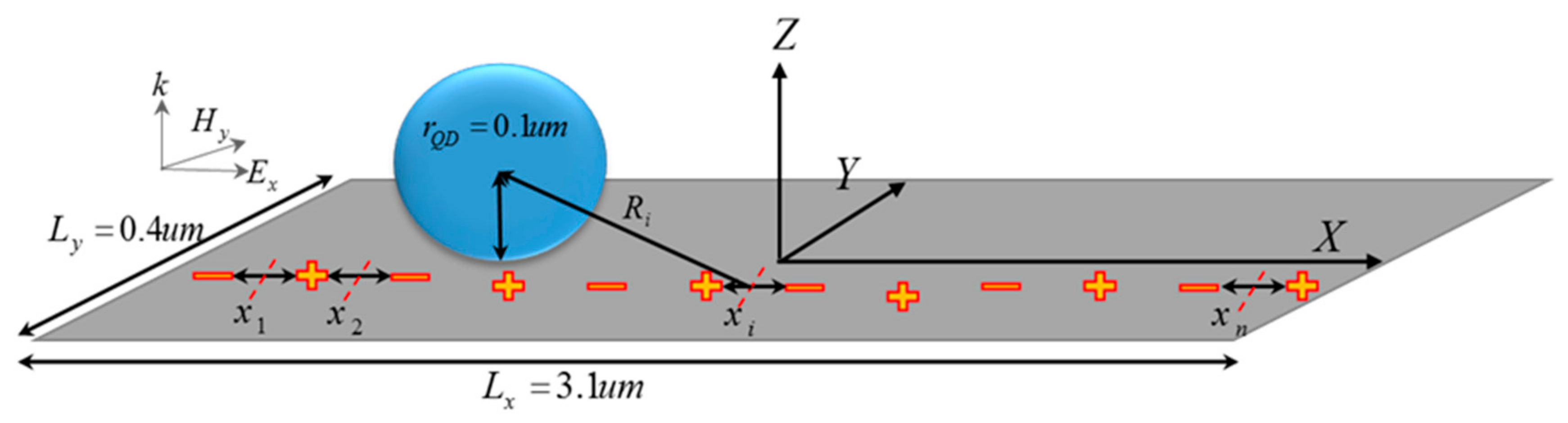
The whole structure under analysis is illustrated in Figure 3, which shows the polarization induced on the surface of the graphene.
The origin of the coordinate system is at the center of the nanoribbon. Additionally, based on plasmon polarization theory, the center of each dipole on the surface is located at . In the equation, is defined as the effective wavelength on the graphene plate [14]. According to Figure 3, the polarization of the graphene nanoribbon was calculated, and was found to be equal to .
2.2. Interaction between the Graphene Nanoribbon and the Quantum Dot
Electromagnetic waves will have significant effects on the two materials in question. In QDs, electromagnetic waves excite excitons, and in the graphene nanoribbon, electrons will be transferred from the lower to the higher excitation level when the frequency of the electromagnetic wave resonates with the QD. This causes a change in the electron cloud, which no longer has a symmetric wave function, resulting in a bipolar momentum. Furthermore, the field on the graphene plate excites the surface plasmon modes. The electrons move in the opposite direction of the field and form a dipole moment that is positive and stationery. Thus, the incident electric field () induces a dipole moment at the quantum dot and forms surface polarizations on the graphene plate as well. It is a given that a dipole structure creates an electric field in its surroundings [6,29], which is calculated separately from the main field. Therefore, the dipole field generated by the graphene nanoribbon in the center of the quantum dot can be calculated in three directions, as follows, which is obtained from the surface plasmons.
where Ri represents the distance between the axis of surface polarization and the center of the quantum dot (), and is the permittivity of the medium surrounding the QD–graphene system.
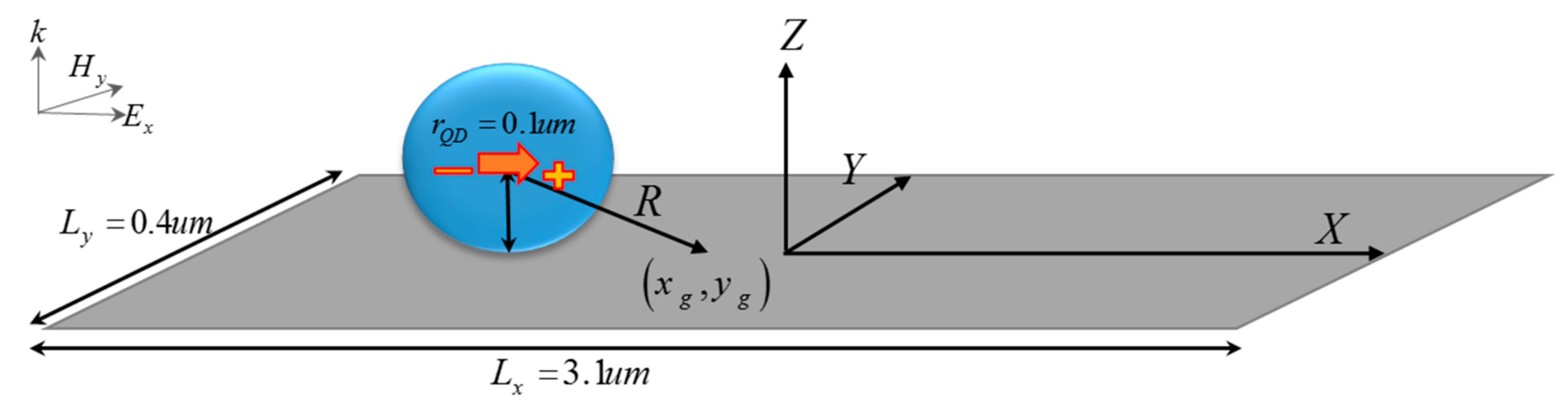
Similarly, the dipole created in the quantum dot induces an electric field around itself. Figure 4 shows the polarization induced in the quantum dot after the input wave is applied. The distance from the dipole in the QD to the point on the graphene plate is represented by R. .
Considering Columbus’s law and the incident applied electric field, the electric field in the surrounding medium induced by the polarization in the QD () can be obtained as follows.
The electric field acting on the graphene nanoribbon is the sum of the applied fields () and the consequent field resulting from quantum dot polarization (). Additionally, the polarization occurring in the quantum dot originates from a set of two fields: the first is the applied electric field (), and the second is the effect of the polariton field of the graphene surface plasmon (). Thus, the total field is the sum of the induced and incident fields.
Here, , and is the permittivity of the quantum dot.
According to the boundary conditions (), the tangential electric fields between these two quantum materials must be equal to each other; therefore, the amount of polarization induced in the quantum dot can be calculated as follows.
Here, we should introduce the constant B. This constant is equivalent to the polarization effect of the graphene surface plasmons on the polarization of the quantum dot, which is referred to as the interaction constant, and which is equivalent to (). According to the amount of polarization obtained in the quantum dot, the total field induced on the graphene nanoribbon can also be obtained. Meanwhile, the susceptibility of the system is obtained on the basis of the polarization of the graphene. The following relation expresses the susceptibility of the structure.
Considering the presented theoretical model, the interaction between the QD and the graphene nanoribbon is modeled. To better understand the formulas and physics of the model, we simulated the results of these calculations numerically, and present the results in the following section.
3. Results
We theoretically studied the interaction of the QD and the graphene nanoribbon in the previous section. To demonstrate this quantitatively, we use numerical calculation. For the evaluation of the system and the numerical study, the input electromagnetic field amplitude was 1 (V/m). The graphene nanoribbon had a thickness of 1 nm and an area of 3100 × 400 nm2. Additionally, the QD had a different radius of around 100 nm. Interaction between these materials in the presence of an input electric field excites the surface plasmon waves on the graphene nanoribbon. The geometry of the graphene nanoribbon and the frequency and amplitude of the input electromagnetic field are basic factors in the strength of the surface plasmon waves.
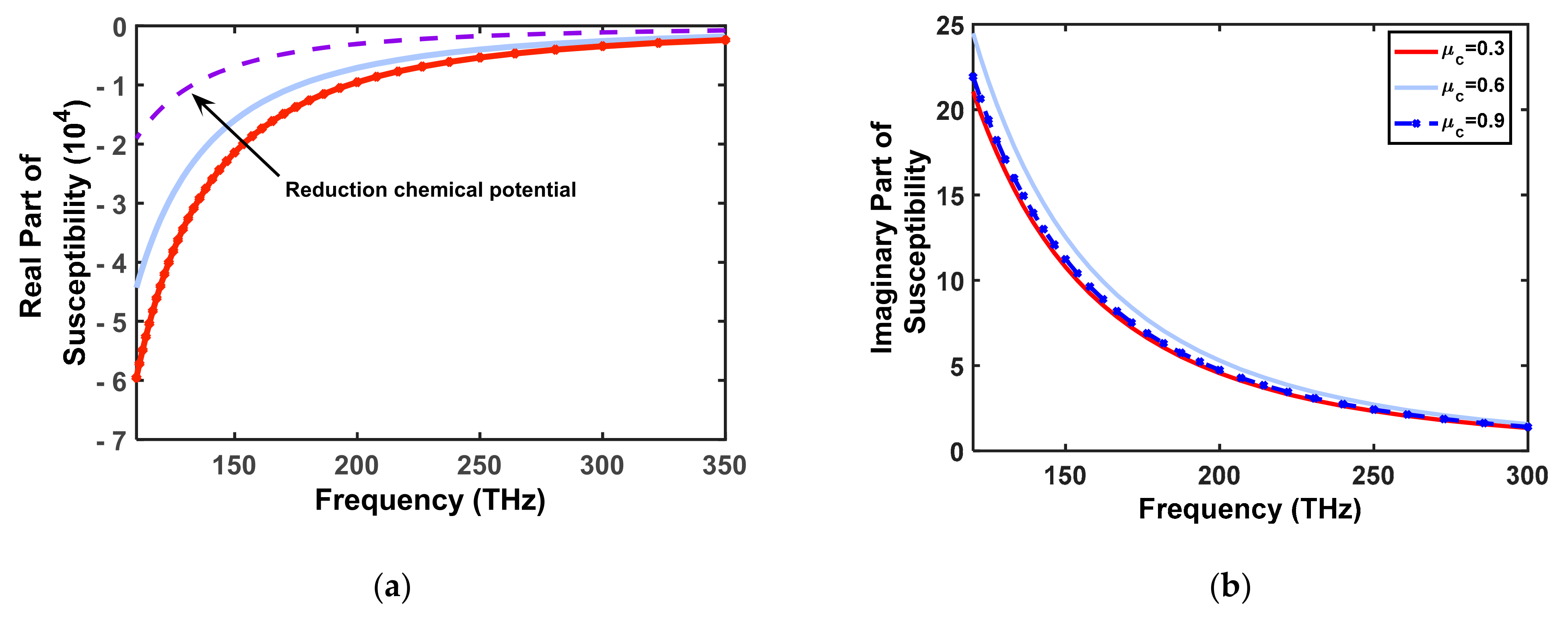
Therefore, the susceptibility of the structure considering Equation (8) is frequency dependent, as shown in Figure 5.
Susceptibility has two parts, real and imaginary (Equation (8)), which express the effective refractive index and absorption coefficient in the structure. Figure 5 considers three different values for the chemical potential, a quantum dot with a radius of 100 nm, and a dielectric constant of 12. Figure 5 shows that variation in the chemical potential has a negligible effect on the imaginary part, while its effect on the real part is significant. It can be seen that when varying the Fermi level or introducing electrons onto the surface of the graphene, the refractive index of the structure changes and is adjusted.
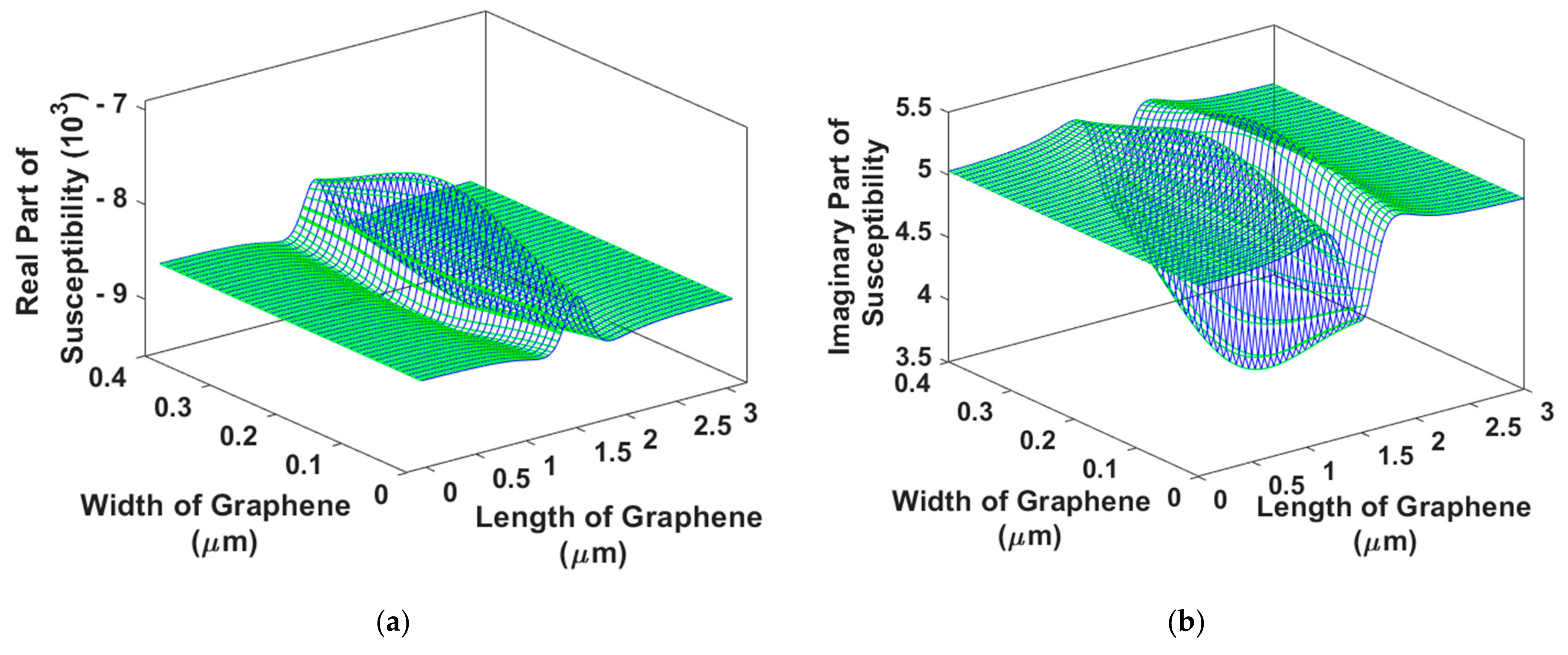
Since the induced electric field on graphene by QD is position dependent, the optical properties of the nanoribbon, such as susceptibility, will also be position dependent. This phenomenon is illustrated in Figure 6. This is a three-dimensional curve that shows the real and imaginary parts of susceptibility versus the length and width of the graphene.
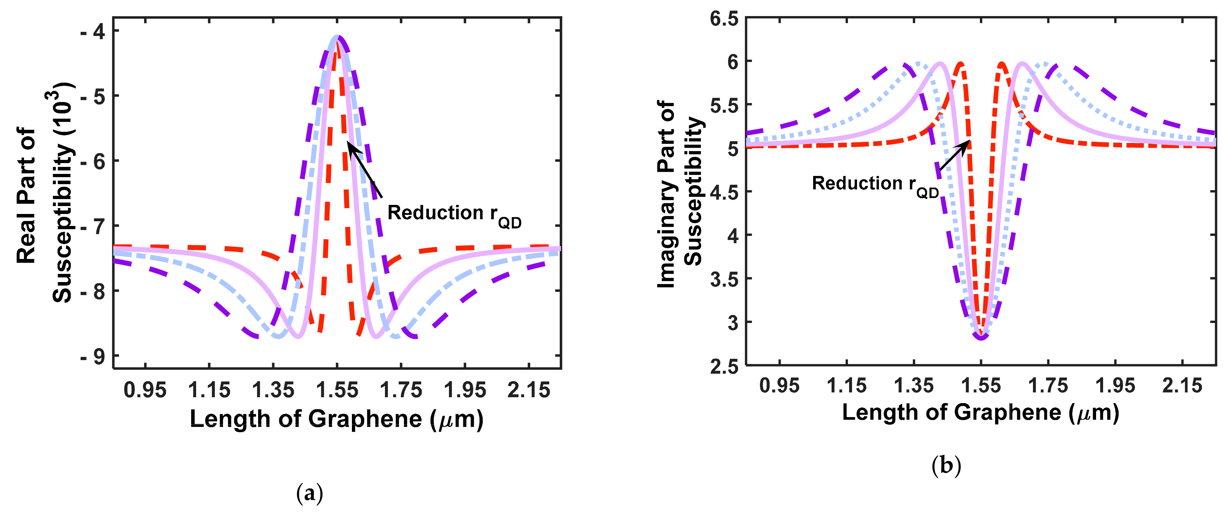
It is notable that the susceptibility is position dependent. For simplicity, it is assumed that the QD’s position changes on the central line of the graphene nanoribbon. Additionally, Figure 7 illustrates the effect of the radius of the QD on susceptibility. In graphene, the amount of the Fermi layer is also important.
The simulated results show that the real and imaginary parts of the susceptibility are localized, and narrow with decreasing QD radius. This is related to the polarization induced by the QD on graphene nanoribbon. The real and imaginary parts have maximum and minimum values, depending on the location of the QD.
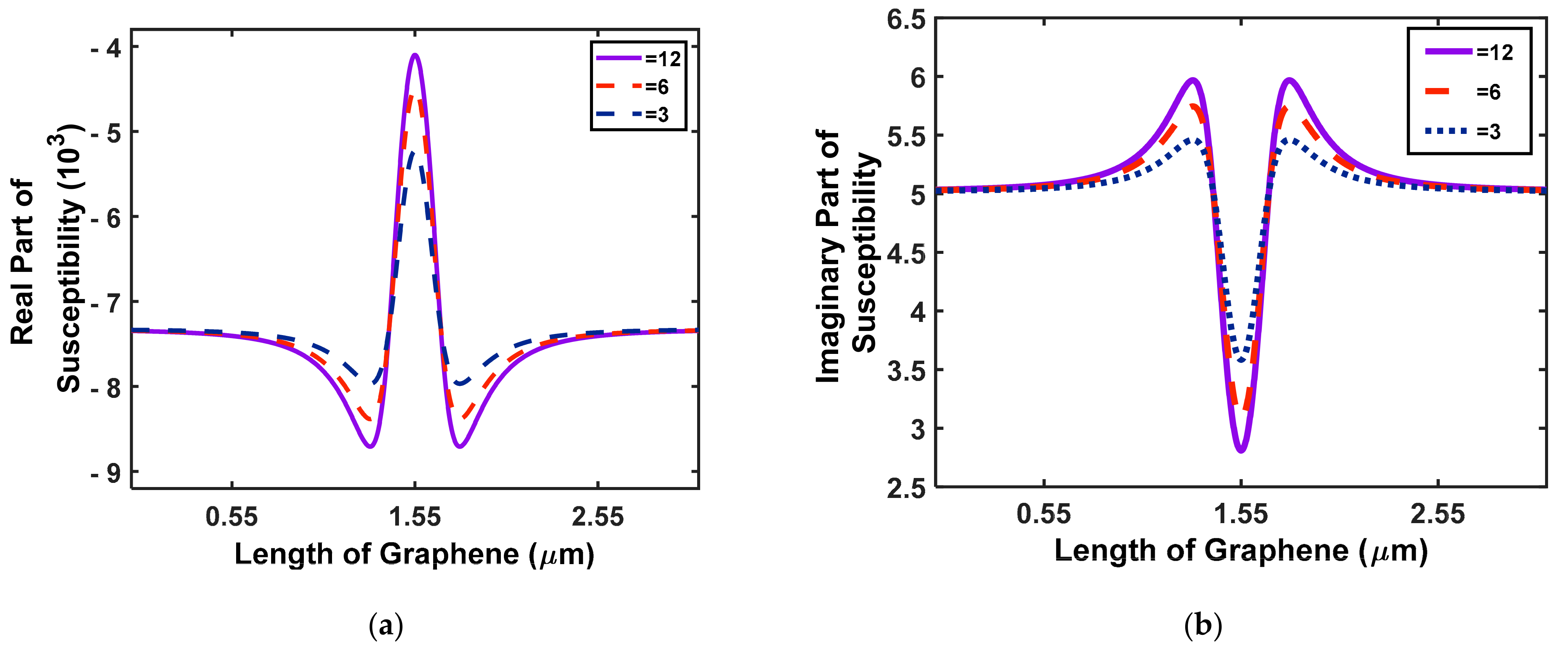
Figure 8a,b show the effect of the permittivity of the quantum dot on susceptibility by changing the material type. It can be observed that when quantum dots with a smaller dielectric coefficient are used, the amplitude of the susceptibility peaks decreases. The dielectric coefficient represents the degree of polarization of the material [2]. Materials with a higher dielectric coefficient will have a higher degree of polarization, and eventually, the field they induce will be larger [2]. It is worth mentioning that when changing the permittivity of the graphene, the induced field and the susceptibility of the QD will change in a manner similar to the previous case.
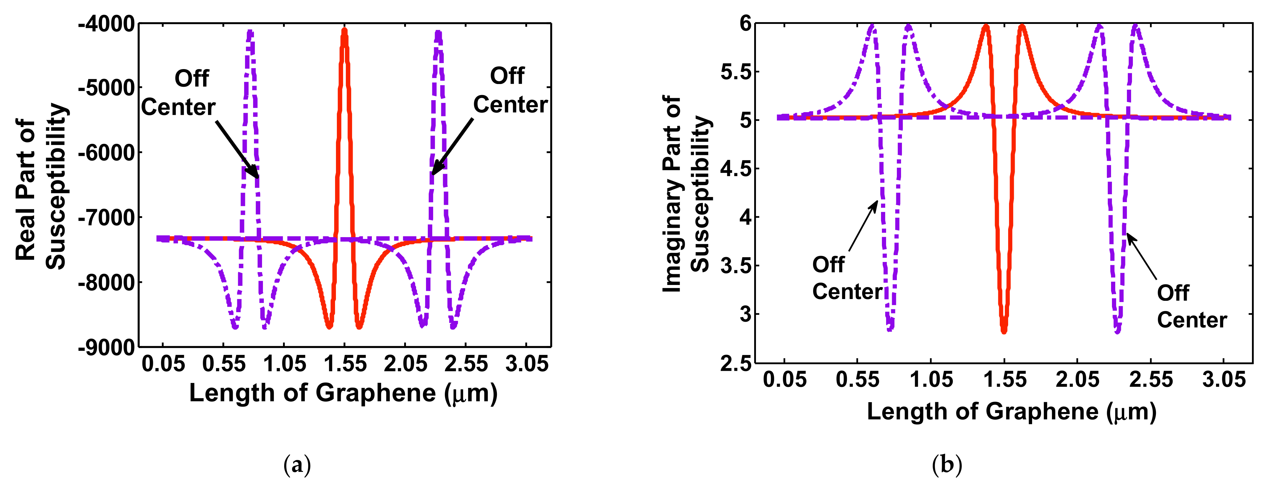
The location of the quantum dot has an effect on the amount of field induced on the graphene plate. Therefore, we move the quantum dot along the x- and y-axes, and determine the way in which the susceptibility changes. The results are reported in Figure 9 and Figure 10. Figure 10 depicts the effect on susceptibility of moving the QD along the y-axis.
As shown in Figure 9, when the distance of the QD from the center of the graphene () nanoribbon increases, the susceptibility decreases. It should be mentioned that the maximum peak is displaced from the center of the nanoribbon to the center of the QD.
By changing the location of the quantum dot on the x-axis (the central length of the nanoribbon) and in three different places (), the susceptibility is calculated, as shown in Figure 10. Considering Figure 3 and the coordinate system, the origin of the coordinate system was placed at the center of the quantum dot. The quantum dot is moved along the x-axis (while in the y-direction, it remains in the center of the nanoribbon). As the quantum dot moves along the x-axis, the susceptibility of the system shifts in the same direction.
There are three maximums for susceptibility, depending on the position of the QD.
As shown in Figure 10, the susceptibility only shifts in the direction of the location of the quantum dot. This characteristic may serve as a tool for realizing periodic quantum structures and facilities for studying the optical and electrical properties of different periodic and aperiodic quantum nanophotonic structures.
4. Discussion
In this work, using numerical simulation, we showed that placing a QD on a graphene nanoribbon is a way to manage the optical and electrical properties of these 2D materials. The physics of the system involve dipole–dipole interactions between the QD and the graphene nanoribbon. Inserting a QD on a graphene nanoribbon changes the electron distribution on the graphene. Therefore, the optical and electrical properties change, and can be controlled. In Figure 1, the dispersion property of graphene nanoribbon is demonstrated. Since the graphene nanoribbon has a lot of free carriers, it is clear that the optical and mechanical properties show dispersion behavior and are frequency dependent. This property can be described by the harmonic oscillator model for electrons. In Figure 2, the chemical potential frequency dependency is demonstrated. Based on the above-mentioned description, the frequency dependency is acceptable.
In Figure 5, the effect of the chemical potential on susceptibility is presented, and it is shown that with increasing chemical potential, the density of free electrons above the Fermi level decreases and so the real part of the susceptibility increases too, and in this case, the graphene nanoribbon operates as a semiconductor.
In Figure 6, the effect of the dimensions of the graphene nanoribbon on its optical properties is studied and demonstrated.
In Figure 7, the effect of the radius of the QD on susceptibility is demonstrated, and it is shown that when the radius is decreased, and the susceptibility is perturbed a little, but this is only limited to QD’s area. It is clear that when the radius is low, the penetration distance of the dipole effect decreases.
In Figure 8, the effect on the susceptibility of the system of the QD consisting of a material type with higher permittivity is studied, and it is shown that with increasing permittivity of the QD, there is an increase in the susceptibility of the system, too. It can be concluded that with increasing permittivity of the QD, the induced polarization on graphene nanoribbon increases, too, because the dipole moment of the QD is greater than in cases with lower permittivity.
Figure 9 and Figure 10 present the effect of the QD’s displacement on the susceptibility of the system. It is shown that with the displacement of the QD along the axis of the graphene nanoribbon, the susceptibility shifts in that direction. It is well known that the cause of perturbation is the QD, and so we expect that when displacing the QD, the susceptibility will be displaced with respect to the normal situation.
In order to validate the present work, it is necessary to provide a detailed explanation. In paper [30], we demonstrated that if a molecule is placed on a graphene layer, the mechanical, electrical, and optical properties change. In Figure 1, it can be seen that the surface of the graphene layer changes. In Figure 2b, it can be seen that the density of the states changes, and so the optical properties must also change. These results were simulated by the Material studio. Then, these results were validated by experiment, and the results are shown in Figure 4. Thus, it was proved that a molecule on the graphene layer causes changes in electrical, optical, and mechanical properties, because the density of states changes.
In [31], noncovalent functionalization of graphene with various species, including biomolecules, polymers, quantum dots, and metals, was investigated for use in energy materials, biosensing, and biomedical applications.
In Figure 13, the force between graphene and species was calculated. This force is due to dipole–dipole interaction. Thus, the existence of the force in Figure 13 validates the proposed theoretical work modeling the interaction between QDs and graphene. In Figure 14, it can be seen that the Raman spectra of the system change when a specimen is placed on the graphene layer. This is another validation of our work. We modeled exactly how this interaction is able to describe these effects.
In [32], the dipole–dipole interaction was used to describe the effect of Au nanoparticles on graphene, and this provided another validation of our theoretical approach.
In [33], which is a review paper, experimental and theoretical methods for the functionalization of the graphene layer were investigated, and the electrical properties of the modified graphene were investigated. In this paper, it was shown that covalent and noncovalent modification have different effects on the optical and electrical performance of the system.
In [34], the effect of an organic molecule on the graphene layer was theoretically investigated. It was shown that P-type graphene can be obtained by means of charge transfer between graphene and an organic molecule. In this work, it was shown that the density of states changes (Figure 4) after placement of an organic molecule on the graphene. This paper provides another validation of our theoretical work in light of the reported results describing the variation of the density of states.
5. Conclusions
In this work, we numerically studied the proposed structure, and the interaction between graphene nanoribbon and a quantum dot was modeled as a dipole–dipole. An analytical formulation for evaluating the optical and electrical properties of the graphene nanoribbon and QDs was introduced. The results showed that the placement of quantum dots on graphene nanoribbon causes the linear susceptibility of the complex structure to change. Considering the physics of operation as well as mathematical modeling, we were able to analyze and describe the interaction between graphene nanoribbons and QDs. The results showed that the perturbation in optical susceptibility was due to the QD, and with the displacement of QD location, the susceptibility shifted too. Additionally, it was shown that the physical parameters of QDs, including geometrical and optical parameters, strongly affect the susceptibility of the system. It was shown that when the QD’s radius and permittivity were increased, the width and amplitude of the susceptibility increased.
This event showed that the periodic and aperiodic optical structures of the quantum systems are practical. Using the type and number of QDs on the graphene nanoribbon, the periodicity and contrast of the refractive index can be managed.
Author Contributions
S.A. write the paper and simulated the task. A.R. designed the project conceptually and write and edit the paper and supervise the project. P.M. writes and edits the paper. All authors have read and agreed to the published version of the manuscript.
Funding
There is no funding for this project.
Institutional Review Board Statement
It does not apply to this paper.
Informed Consent Statement
It does not apply to this paper.
Data Availability Statement
There is no data in this paper to publish.
Conflicts of Interest
The authors declare no conflict of interest.
References
- Bozhevolnyi, S.I.; Martin-Moreno, L.; Garcia-Vidal, F. Quantum Plasmonics; Springer: Berlin/Heidelberg, Germany, 2017. [Google Scholar]
- Luther, J.; Jain, P.; Ewers, T.; Alivisatos, P. Localized surface plasmon resonances arising from free carriers in doped quantum dots. Nat. Mater. 2011, 10, 361–366. [Google Scholar] [CrossRef]
- Sadeghi, S.M.; Deng, L.; Li, X.; Huang, W.P. Plasmonic (thermal) electromagnetically induced transparency in metallic nanoparticle–quantum dot hybrid systems. Nanotechnology 2009, 20, 365401. [Google Scholar] [CrossRef]
- Artuso, R.D.; Bryant, G.W. Strongly coupled quantum dot-metal nanoparticle systems: Exciton-induced transparency, discontinuous response, and suppression as driven quantum oscillator effects. Phys. Rev. B 2010, 82, 195419. [Google Scholar] [CrossRef]
- Gubin, M.Y.; Prokhorov, A.V.; Volkov, V.S.; Evlyukhin, A.B. Controllable Excitation of Surface Plasmon Polaritons in Graphene-Based Semiconductor Quantum Dot Waveguides. Annalen Physik 2021, 533, 2100139. [Google Scholar] [CrossRef]
- Cox, J.D.; Singh, M.R.; Gumbs, G.; Anton, M.A.; Carreno, F. Dipole-dipole interaction between a quantum dot and a Graphene nanodisk. Phys. Rev. B 2012, 86, 125452. [Google Scholar] [CrossRef] [Green Version]
- Ogawa, S.; Fukushima, S.; Shimatani, M. Graphene Plasmonics in Sensor Applications: A Review. Sensors 2020, 20, 3563. [Google Scholar] [CrossRef] [PubMed]
- Plesco, I.; Dragoman, M.; Strobel, J.; Ghimpu, L.; Schütt, F.; Dinescu, A.; Ursaki, V.; Kienle, L.; Adelung, R.; Tiginyanu, I. Flexible pressure sensor based on Graphene aerogel microstructures functionalized with CdS nanocrystalline thin film. Superlattices Microstruct. 2018, 117, 418–422. [Google Scholar] [CrossRef]
- Armaghani, S.; Khani, S.; Danaei, M. Design of all-optical Graphene switches based on a Mach-Zehnder interferometer employing optical Kerr effect. Superlattices Microstruct. 2019, 135, 106244. [Google Scholar] [CrossRef]
- Kimmitt, N.; Wertz, E.A. Tracking the Coupling of Single Emitters to Plasmonic Nanoantennas with Single-Molecule Super-Resolution Imaging. ACS Photonics 2021, 8, 1020–1026. [Google Scholar] [CrossRef]
- Kok, P.; Lovett, B.W. Introduction to Optical Quantum Information Processing; Cambridge University Press: Cambridge, UK, 2010. [Google Scholar]
- Gonzalez-Tudela, A.; Cano, D.M.; Moreno, E.; Martín-Moreno, L.; Tejedor, C.; Garcia-Vidal, F.J. Entanglement of two qubits mediated by one-dimensional plasmonic waveguides. Phys. Rev. Lett. 2011, 106, 020501. [Google Scholar] [CrossRef]
- Kawata, S. Plasmonics: Future outlook. Jpn. J. Appl. Phys. 2012, 52, 010001. [Google Scholar] [CrossRef] [Green Version]
- Maier, S.A. Plasmonics: Fundamentals and Applications; Springer: Berlin/Heidelberg, Germany, 2007; Volume 1. [Google Scholar]
- West, P.; Ishii, S.; Naik, G.; Emani, N.K.; Shalaev, V.; Boltasseva, A. Searching for better plasmonic materials. Laser Photonics Rev. 2010, 4, 795–808. [Google Scholar] [CrossRef] [Green Version]
- Sun, Z.; Martinez, A.; Wang, F. Optical modulators with 2D layered materials. Nat. Photonics 2016, 10, 227–238. [Google Scholar] [CrossRef] [Green Version]
- Gao, Z.; Wu, L.; Gao, F.; Luo, Y.; Zhang, B. Spoof plasmonics: From metamaterial concept to topological description. Adv. Mater. 2018, 30, 1706683. [Google Scholar] [CrossRef]
- Luo, X. Engineering optics 2.0: A revolution in optical materials, devices, and systems. ACS Photonics 2018, 5, 4724–4738. [Google Scholar] [CrossRef]
- Vakil, A. Transformation Optics Using Graphene: One-Atom-Thick Optical Devices Based on Graphene; University of Pennsylvania: Philadelphia, PA, USA, 2012. [Google Scholar]
- Wu, J.; Gong, M.; Schmitz, R.C.; Liu, B. Quantum Dot/Graphene Heterostructure Nanohybrid Photodetectors. In Quantum Dot Photodetectors; Springer: Berlin/Heidelberg, Germany, 2021; pp. 215–248. [Google Scholar]
- Vakil, A.; Engheta, N. Transformation optics using Graphene. Science 2011, 332, 1291–1294. [Google Scholar] [CrossRef] [Green Version]
- Amirhosseini, A.A.; Safian, R. A hybrid plasmonic waveguide for the propagation of surface plasmon polariton at 1.55 μm on SOI substrate. IEEE Trans. Nanotechnol. 2013, 12, 1031–1036. [Google Scholar] [CrossRef]
- Ban, X.; Zhong, M.; Little, B.E. Broadband hybrid plasmonic Graphene modulator operating at mid-Infrared wavelength. Optik 2021, 247, 168036. [Google Scholar] [CrossRef]
- Liu, P.; Zhang, X.; Ma, Z.; Cai, W.; Wang, L.; Xu, J. Surface plasmon modes in Graphene wedge and groove waveguides. Opt. Express 2013, 21, 32432–32440. [Google Scholar] [CrossRef]
- Gu, X.; Lin, I.-T.; Liu, J.-M. Extremely confined terahertz surface plasmon-polaritons in Graphene-metal structures. Appl. Phys. Lett. 2013, 103, 071103. [Google Scholar] [CrossRef]
- Gan, C.H.; Chu, H.S.; Li, E.P. Synthesis of highly confined surface plasmon modes with doped Graphene sheets in the midinfrared and terahertz frequencies. Phys. Rev. B 2012, 85, 125431. [Google Scholar] [CrossRef] [Green Version]
- Hosseininejad, S.E.; Komjani, N.; Noghani, M.T. A comparison of Graphene and noble metals as conductors for plasmonic one-dimensional waveguides. IEEE Trans. Nanotechnol. 2015, 14, 829–836. [Google Scholar] [CrossRef]
- Jovanović, V.B.; Radovic, I.; Borka, D.; Mišković, Z.L. High-energy plasmon spectroscopy of freestanding multilayer Graphene. Phys. Rev. B 2011, 84, 155416. [Google Scholar] [CrossRef] [Green Version]
- Engheta, N.; Ziolkowski, R.W. Metamaterials: Physics and Engineering Explorations; John Wiley & Sons: Hoboken, NJ, USA, 2006. [Google Scholar]
- Siahsar, M.; Jabbarzadeh, F.; Dolatyari, M.; Rostami, G.; Rostami, A. Fabrication of highly sensitive and Fast Response MIR Photodetector based on a New Hybrid Graphene Structure. Sens. Actuators A Phys. 2016, 238, 150–157. [Google Scholar] [CrossRef]
- Georgakilas, V.; Tiwari, J.N.; Kemp, K.C.; Perman, J.A.; Bourlinos, A.B.; Kim, K.S.; Zboril, R. Noncovalent functionalization of graphene and graphene oxide for energy materials, biosensing, catalytic, and biomedical applications. Chem. Rev. 2016, 116, 5464–5519. [Google Scholar] [CrossRef] [Green Version]
- Low, S.; Shon, Y.S. Molecular interactions between preformed metal nanoparticles and graphene families. Adv. Nano Res. 2018, 6, 357–375. [Google Scholar]
- Kuila, T.; Bose, S.; Mishra, A.K.; Khanra, P.; Kim, N.H.; Lee, J.H. Chemical functionalization of graphene and its applications. Prog. Mater. Sci. 2012, 57, 1061–1105. [Google Scholar] [CrossRef]
- Lu, Y.H.; Chen, W.; Feng, Y.P.; He, P.M. Tuning the Electronic Structure of Graphene by an Organic Molecule. J. Phys. Chem. B 2009, 113, 2–5. [Google Scholar] [CrossRef] [Green Version]
Figure 1.
The real part of permittivity versus energy level with the chemical potentials of graphene (chemical potential is increased from 0.1 to 1 eV from left to right).
Figure 1.
The real part of permittivity versus energy level with the chemical potentials of graphene (chemical potential is increased from 0.1 to 1 eV from left to right).

Figure 2.
Chemical potential versus input wave energy in graphene.

Figure 3.
The structure under study with induced polarization.

Figure 4.
The structure under study and the polarization of the quantum dot.

Figure 5.
The real (a) and imaginary (b) parts of susceptibility versus frequency for different values of chemical potential.
Figure 5.
The real (a) and imaginary (b) parts of susceptibility versus frequency for different values of chemical potential.

Figure 6.
(a) Real and (b) imaginary parts of susceptibility for a chemical potential of 0.3.

Figure 7.
Effect of quantum radius on (a) real part and (b) imaginary part of the susceptibility .

Figure 8.
Effect of the permittivity of the quantum dot with radius 100 nm on (a) real and (b) imaginary parts of susceptibility.
Figure 8.
Effect of the permittivity of the quantum dot with radius 100 nm on (a) real and (b) imaginary parts of susceptibility.

Figure 9.
The (a) real and (b) imaginary parts of susceptibility for two different modes of quantum dot .
Figure 9.
The (a) real and (b) imaginary parts of susceptibility for two different modes of quantum dot .

Figure 10.
The (a) real and (b) imaginary parts of susceptibility for different positions of QD ().


Table 1.
Graphene plasmon energy in terms of chemical potential.
| Chemical Potential (eV) | Plasmon Energy (eV) |
|---|---|
| 0.2 | 55.87 |
| 0.4 | 88.22 |
| 0.6 | 104.4 |
| 0.8 | 110 |
| 1 | 121 |
Publisher’s Note: MDPI stays neutral with regard to jurisdictional claims in published maps and institutional affiliations. |
© 2022 by the authors. Licensee MDPI, Basel, Switzerland. This article is an open access article distributed under the terms and conditions of the Creative Commons Attribution (CC BY) license (https://creativecommons.org/licenses/by/4.0/).
Share and Cite
MDPI and ACS Style
Armaghani, S.; Rostami, A.; Mirtaheri, P. Analysis and Simulation of the Optical Properties of a Quantum Dot on a Graphene Nanoribbon System. Photonics 2022, 9, 220. https://doi.org/10.3390/photonics9040220
AMA Style
Armaghani S, Rostami A, Mirtaheri P. Analysis and Simulation of the Optical Properties of a Quantum Dot on a Graphene Nanoribbon System. Photonics. 2022; 9(4):220. https://doi.org/10.3390/photonics9040220
Chicago/Turabian StyleArmaghani, Sahar, Ali Rostami, and Peyman Mirtaheri. 2022. "Analysis and Simulation of the Optical Properties of a Quantum Dot on a Graphene Nanoribbon System" Photonics 9, no. 4: 220. https://doi.org/10.3390/photonics9040220
Note that from the first issue of 2016, this journal uses article numbers instead of page numbers. See further details here.