Communication

Ultrahigh-Q Tunable Terahertz Absorber Based on Bulk Dirac Semimetal with Surface Lattice Resonance

School of Physics and Electronics, Hunan University, Changsha 410082, China
*
Author to whom correspondence should be addressed.
Photonics 2022, 9(1), 22; https://doi.org/10.3390/photonics9010022
Submission received: 7 December 2021 / Revised: 27 December 2021 / Accepted: 29 December 2021 / Published: 31 December 2021
(This article belongs to the Section Optoelectronics and Optical Materials)

Abstract

:
In this paper, we present an easy-to-implement metamaterial absorber based on bulk Dirac semimetal (BDS). The proposed device not only obtains an ultrahigh quality factor (Q-factor) of 4133 and dynamic adjustability at high absorption, but also exhibits an excellent sensing performance with a figure of merit (FOM) of 4125. These outstanding properties are explained by the surface lattice resonance, which allows us to improve the quality factor significantly and control resonance wavelength precisely by tuning the unit cell periods, Fermi energy of the BDS, and structural parameters. Our findings can provide high-performance applications in terahertz filtering, detection, and biochemical sensing.

1. Introduction

Metamaterials are artificial materials with sub-wavelength structures and special electromagnetic properties that cannot be obtained from nature. In 2008, Landy et al. first demonstrated the concept of metamaterial absorber (MA) [1]. Since then, MAs have attracted a great deal of attention from researchers. The diverse MAs have been proposed according to the operating band range of the devices, including microwave [2], terahertz [3], infrared [4], visible range [5], etc. Moreover, the absorption spectra are divided into broadband and narrowband absorbers, classified by their width. Typically, broadband absorptions are commonly used in photovoltaic and solar collections [6]. However, narrowband absorptions have been exceptionally widely used in photodetectors [7], filters [8], and sensors [9]. In particular, due to the low photon energy and non-ionizing properties of terahertz (THz) waves, terahertz narrowband absorption devices based on metamaterials have received increasing attention and have been widely used in filtering, detection, and biochemical sensing [10,11]. For an absorber, the high quality factor (Q-factor) resonance indicates low loss and supports a strong interaction between electromagnetic waves and analytes, showing sensitivity to minute quantities of analytes and weak environment changes [12]. Regrettably, the Q-factor of the reported terahertz absorbers based on metamaterials is significantly tiny due to the weak radiation effects and absorption loss [13,14]. In 2017, Wang et al. proposed an ultra-narrow terahertz perfect absorber based on a metal-dielectric-metal structure, demonstrating surface lattice resonance [15]. It has a unique resonant mode and high sensitivity different from the general electromagnetic mode, providing a critical sensing platform. However, to achieve tunability of the resonance spectroscopy properties, it is necessary to change the geometrical parameters of the MA. The resonance performance of the MA using this kind of design method increases the cost due to the reconfiguration of the structure in practical applications.
Recently, dynamically tunable absorption materials based on three-dimensional bulk Dirac semimetal (BDS) have shown well sensing performance in the terahertz region [16,17]. This passive cost-increasing approach was refined by replacing conventional materials with BDS. 3D BDS, a quantum material state that can be considered “3D graphene”, has recently attracted in-depth research due to its remarkable properties for manipulating electromagnetic waves [18]. Similar to graphene, the permittivity functions of BDS can also be dynamically adjusted by changing Fermi energy through chemical doping and application of a gate voltage, which saves cost and increases work efficiency [16,19,20]. However, compared to graphene, BDS has substantial nonlinear plasmonic properties while retaining the structural advantages of bulk metals, reduced passive plasmonic losses, and easier handling in fabrication facilities [21,22]. Timusk et al. verified the Dirac properties of AlCuFe quasicrystals [23]. Kharzeev et al. found a strong and narrow plasmon excitation in bulk Dirac semimetal [24]. Yang et al. [25] reported that the highly crystalline Dirac semimetal with tunable morphology and thickness could be controllably synthesized by chemical vapor deposition (CVD) growth on the Au substrate. Moreover, they further demonstrated the feasibility of realistic utilization of the high-performance photodetection system at the terahertz band based on the BDS material. Recently, Luo et al. proposed a multi-band tunable perfect absorber with BDS to realize an ultrasensitive tunable sensor [26]. Due to the excellent performance of BDS, it can be used as a promising device for biochemical sensing.
In this paper, we demonstrate a metamaterial absorber with ultrahigh Q-factor based on a BDS cross and an opaque gold layer in the terahertz region. The physical mechanism of narrowband absorption is attributed to the surface lattice resonance by analyzing the electric field distribution. The absorption performance of the device can be manipulated in multiple ways, including changing the period, width, and thickness. Interestingly, active modulation of the incident wave can be achieved by changing the Fermi energy of the BDS. Moreover, the Q-factor of the device can be significantly improved by reducing the thickness of the BDS. At a certain small thickness, the Q-factor of the proposed device up to 4133 can be obtained. In addition, the absorber has an outstanding biochemical sensing performance with a figure of merit (FOM) of up to 4125 at this specific thickness. These results may provide a new guideline for designing ultra-narrowband absorbers and sensors in the future.

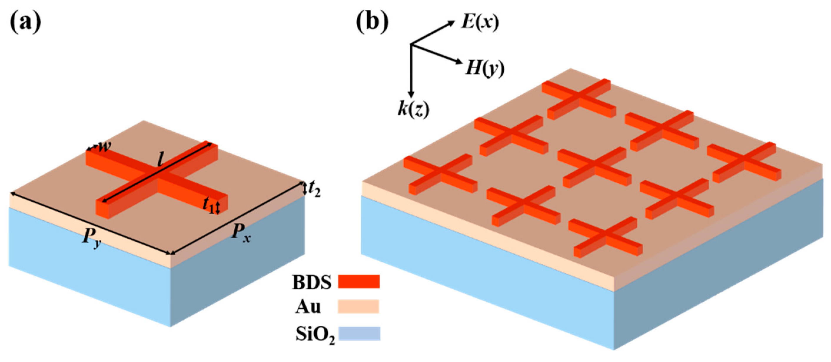
2. Structures and Methods

The sketches of the metamaterial absorber that we propose are shown in Figure 1a,b. The proposed device consists of a BDS cross-shaped patch on the topside and a continuous gold film at the bottom. The absorber is placed on the silicon dioxide (SiO2) substrate. To ensure that the structure works in reflection mode, we make the thickness t2 of gold (Au) equal to 4 μm over the skin depth. The Drude model describes Au with a plasma frequency fp = 2181 THz and a damping constant fτ = 6.5 THz [27]. The proposed structure is simulated using periodic boundary conditions in the x and y directions with Px = Py = P. The length, width, and thickness of BDS are set to l, w, t1. The conductivity σ of BDS can be derived by the random-phase approximation theory [28]:
Re { σ ( Ω ) } = e 2 q k F 24 π Ω G ( Ω / 2 )
Im σ ( Ω ) = e 2 q k F 24 π 2 { 4 Ω [ 1 + π 2 3 ( T E F ) 2 ] + 8 Ω 0 ε c [ G ( ε ) G ( Ω / 2 ) Ω 2 4 ε 2 ] ε d ε }
where G(E) = n(−E) − n(E) with n(E) is the Fermi distribution function, q is the degeneracy factor. kF = EF/ħvF is the Fermi momentum, vF = 106 m/s means Fermi velocity, and EF is the Fermi energy. ε = E/EF, Ω = ħω/EF + iħτ−1/EF, εc = Ec/EF, (Ec is the cutoff energy). Correspondingly, the permittivity of BDS can be expressed as [18]:
ε ( ω ) B D S = ε b + i σ ( ω ) / ω ε 0
where ε0 is the permittivity of the vacuum. In our model, we set εb = 1, q = 40 for AlCuFe quasicrystals [23].Figure 2a,b shows the variation of the real and imaginary parts of the permittivity with the wavelength at different Fermi energies of the BDS. In this paper, the 3D finite-difference time-domain (FDTD) is employed to obtain the simulation results. A plane beam polarized along the x-direction is vertically incident on the absorber, as shown in Figure 1b. Periodic boundary conditions are used in the x and y directions, while the perfectly matched layer (PML) is used in the z-direction. In addition, the electric field distribution is displayed in near-field conditions to indicate resonance patterns. At the same time, transmission and reflection are calculated in far-field conditions to reveal the physical mechanisms.

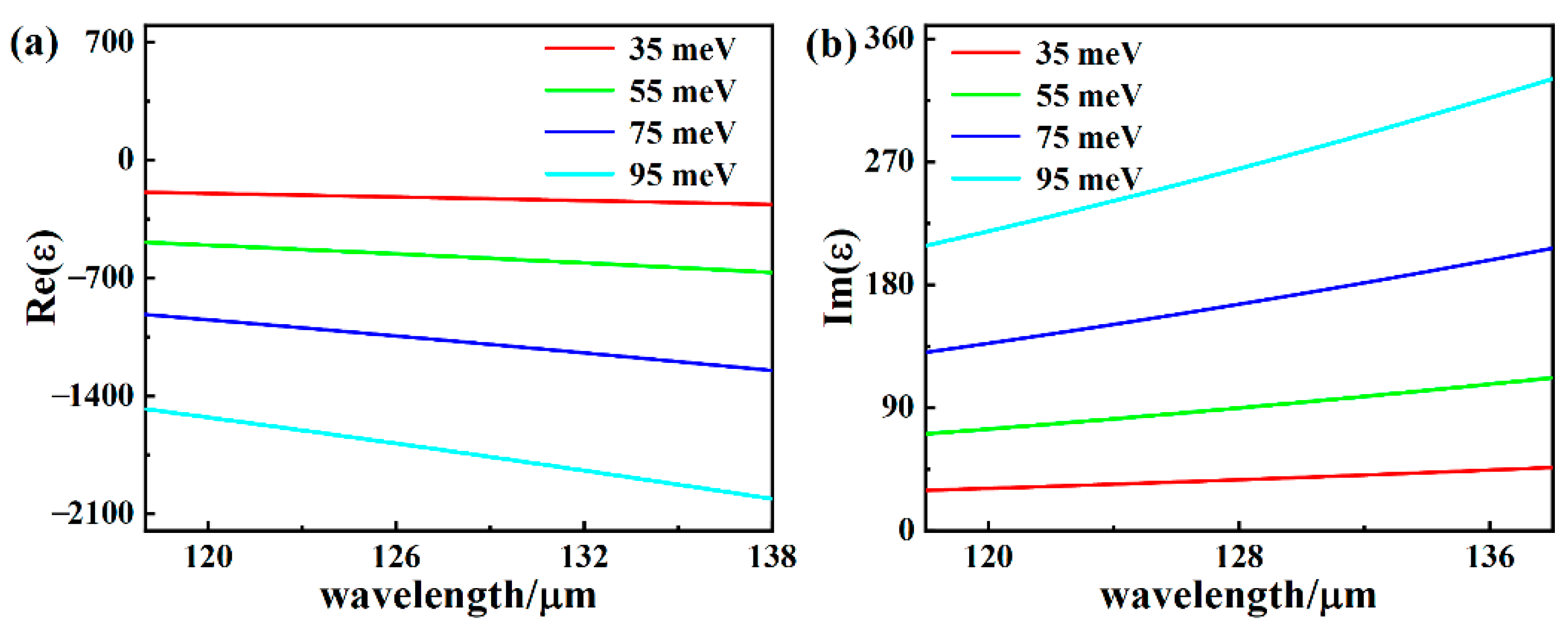
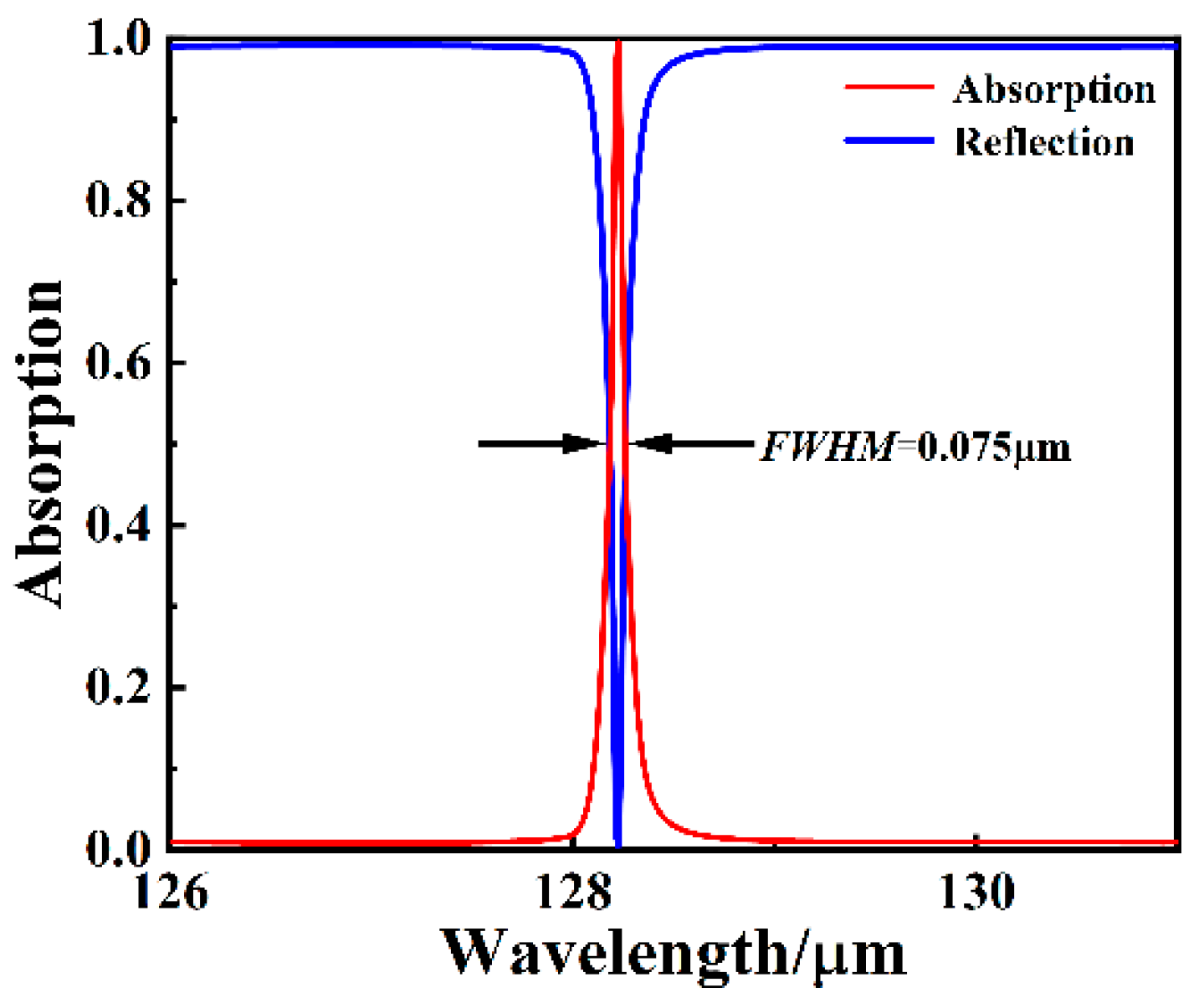
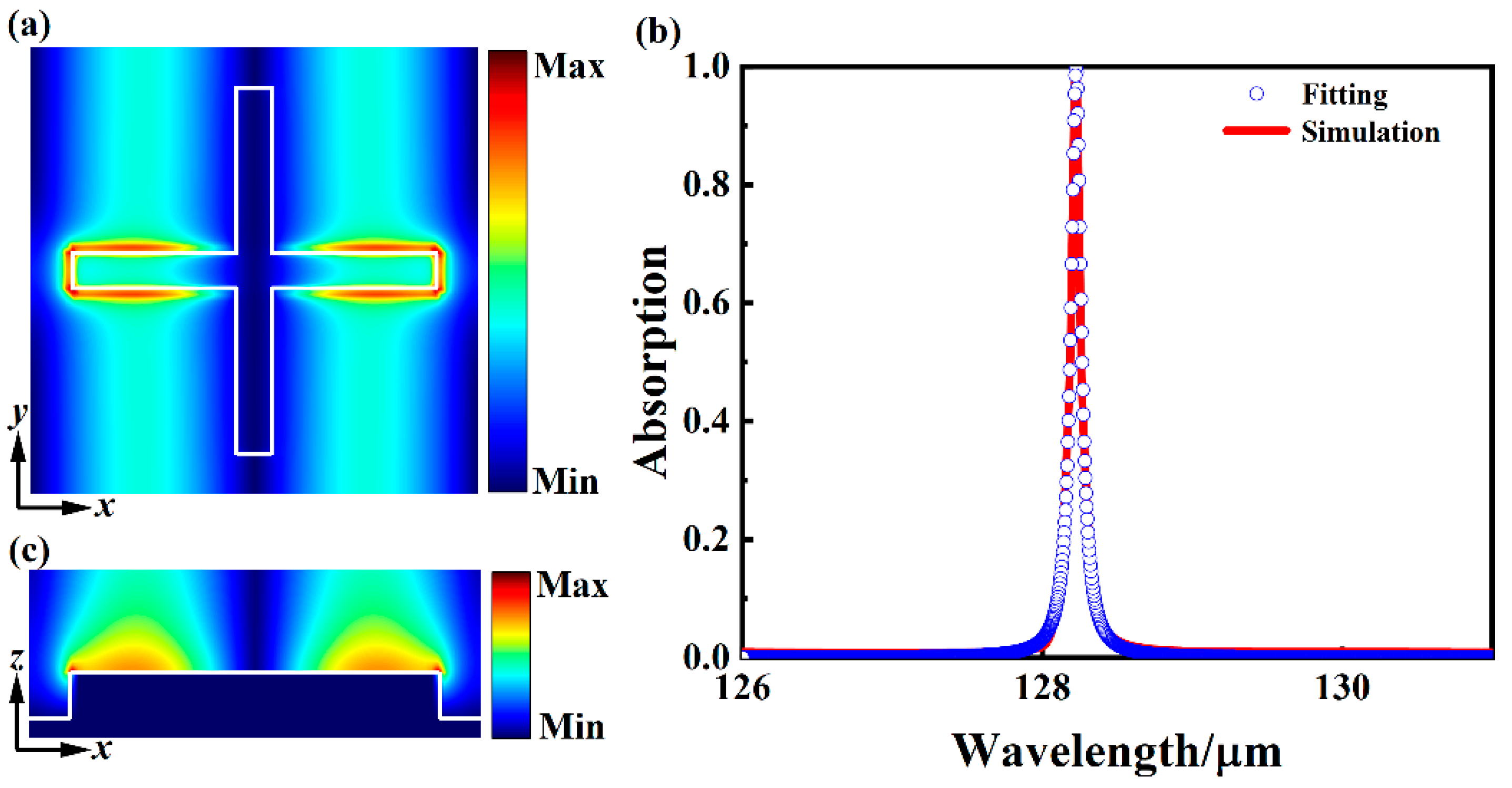
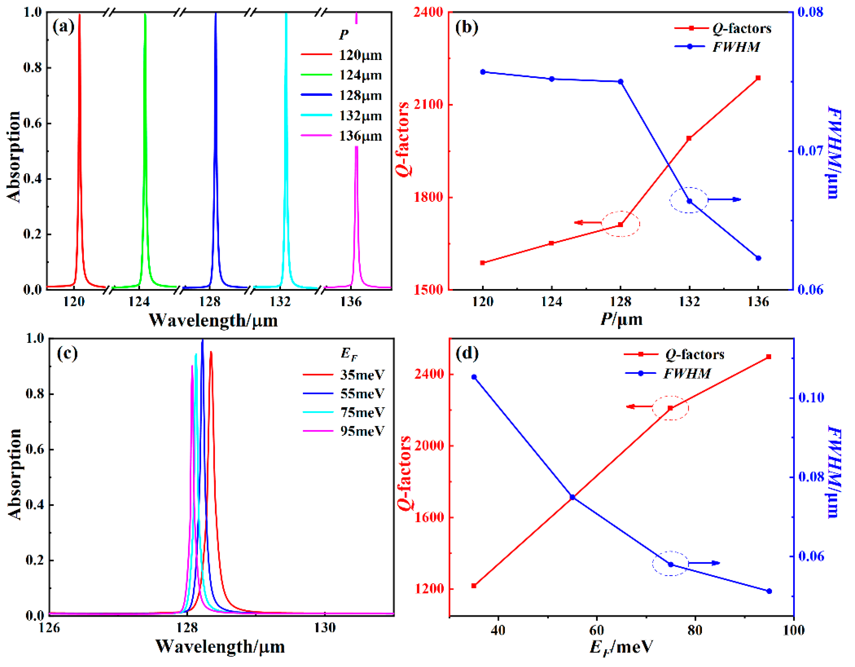
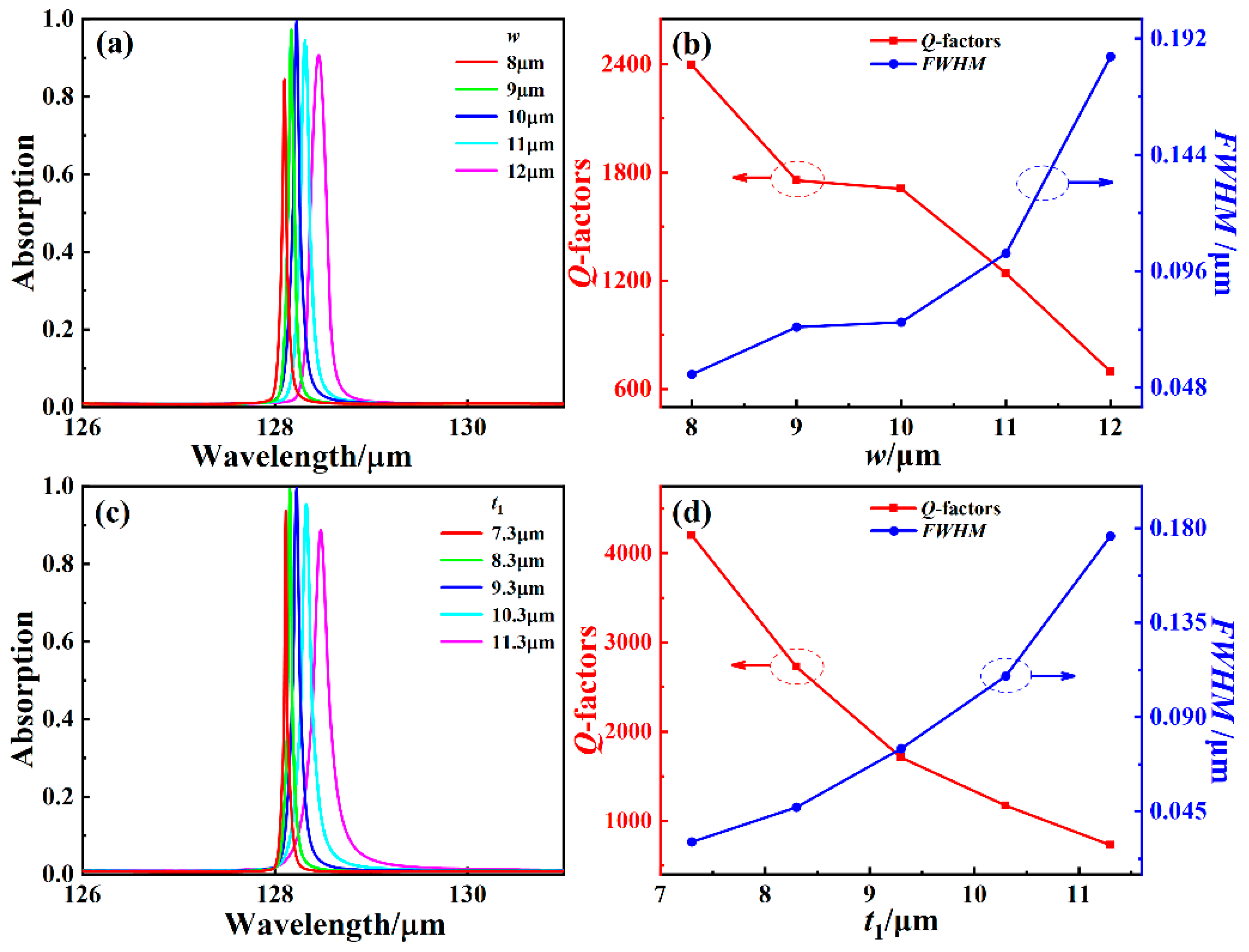
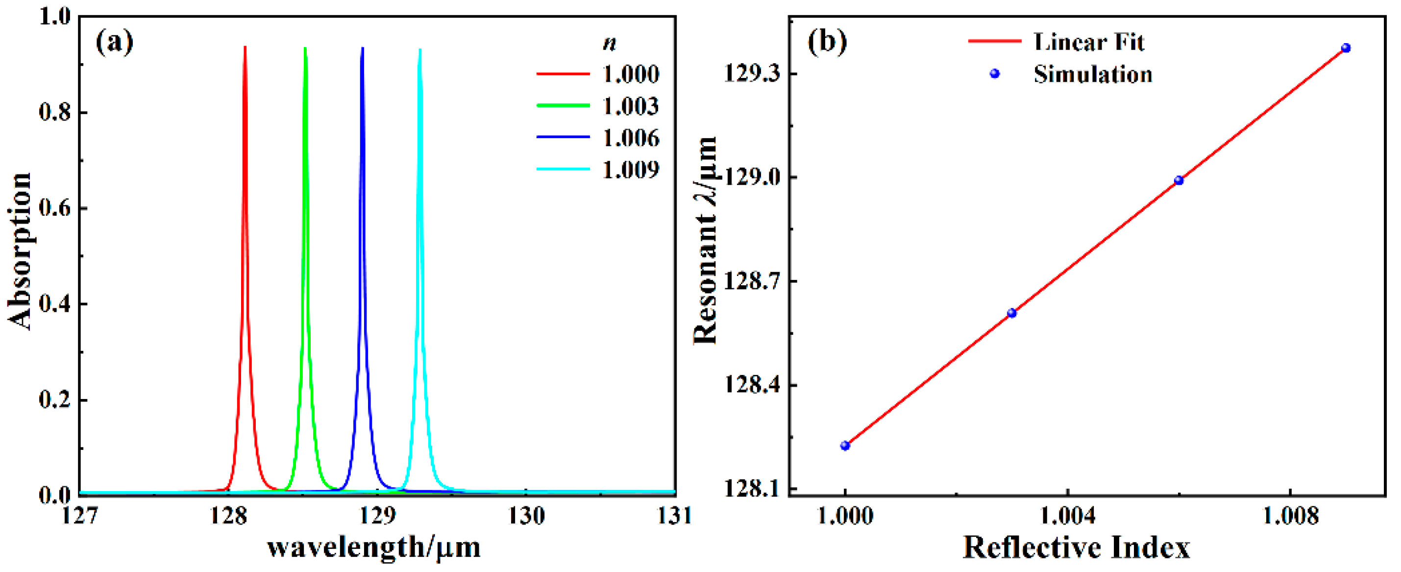
3. Results and Discussion

To understand the physical mechanisms and performances of the absorber, as shown in Figure 1a, the geometric parameters are set as follows: P = 128 μm, l = 105 μm, w = 10 μm, t1 = 9.3 μm, t2 = 4 μm. The Fermi energy (EF) of BDS is 55 meV. Unless otherwise specified, these parameters remain unchanged. The absorptivity (A) of the narrowband near-perfect absorber is calculated using A = 1 − TR, where T and R are the transmission and reflection of the device, respectively. Since the thickness of the opaque gold layer is greater than the skinning depth, the transmission of the proposed absorber is suppressed (T = 0), which makes absorptivity (A) expressed as 1 − R. Moreover, the reflection R can be suppressed by optimizing the impedance of the absorber. As shown in Figure 3, the absorption and reflection spectra of the absorber are indicated by the red and blue lines, respectively. A prominent resonance absorption peak is obtained at a wavelength of λ0 (128.225 μm) with an absorption rate of 99.48%, achieving a near-perfect narrowband spectrum. The quality factor (Q-factor) is defined as Q = λ0/FWHM, where λ0 is the resonance wavelength, FWHM is the full width at half maximum. Of note, the FWHM of the absorption spectrum (λ0 = 128.225 μm) is only 0.075 μm, and the corresponding Q-factor is as high as 1710. To clarify the characteristics of the resonance mode, Figure 4a,c shows the electric field (|E|) distribution at the resonance wavelength λ0 of the x-y plane and the x-z plane, respectively. The electric field is mainly distributed at the edge of the BDS cross in the x-direction and only supports the dipole resonance, which presents the characteristics of the localized distribution. The electric field distribution shows that the micron structure prepared on the gold film can stimulate strong absorption resonance and produce strong electric field localization at the interface between BDS and air, which is a typical surface lattice resonance (SLR) [15,29,30].
As described above, the near-perfect absorption occurs in the SLR band. Therefore, the resonance wavelength can be adjusted by the unit period of the device. In the BDS cross arrays, diffraction will lead to a strong interaction when the grating order changes from evanescent to radiative. The resonance wavelength can be obtained by the following formula [30,31,32,33,34]:
λ ( i , j ) = n i 2 P x 2 + j 2 P y 2
where n is the refractive index around the resonant device, (i,j) represents the grating diffraction order, and Px and Py are the unit period in the x and y directions, respectively. In our simulation, n = 1 (the device is located in the air), Px = Py = P. According to formula (4), the first grating order in the air changes from evanescent to radiative when λ(0,1) = P = 128 μm. Remarkably, the resonance wavelength of the ultra-narrow absorber device is about 128.225 μm, which is very close to the period P (128 μm). The above result shows that the resonance wavelength is mainly determined by the diffraction mode, and the physical origin of the metamaterial absorber is caused by SLR. A slight displacement of 0.225 μm between the simulated formant position and the theoretical value is due to the resonance displacement caused by the plasmonic coupling between adjacent BDS crosses. Moreover, the absorption spectrum of the resonant device based on SLR can be described by the following Lorentz line shape in the frequency domain [30,31,35]:
L ( f ) = L 0 + 2 A π m 4 ( f f 0 ) 2 + m 2
where f is the frequency, f0 is the resonance frequency, and m is the FWHM in frequency. As shown in Figure 4b, the Lorentz fitting results under period P = 128 μm shown by the blue dotted line are well matched to the simulation results in the red curve. It provides additional evidence that the physical mechanism of the proposed device is SLR.
To better understand the mechanism of narrowband absorption, the effects of device parameters changes are investigated. Simulation absorption of the designed device with changes in the unit period P is illustrated in Figure 5a,b. Due to the resonance mechanism of the proposed device which is based on SLR, the resonance wavelength is mainly determined by the period P according to formula 4. As shown in Figure 5a, when the period P varies from 120 to 136 μm with an interval of 4 μm, the resonant wavelength is very close to the size of the corresponding period P, while maintaining an absorption of more than 99%. By properly adjusting the period P, the absorption spectra of the device can achieve resonance at the specified position, which makes the device have great potential applications in filtering and detection. At the same time, we find that as period P increases, the Q-factor of the absorber increases from 1588 to 2186 due to the decrease of FWHM, as shown in Figure 5b. Based on the above result, the absorption performance can be improved by appropriately increasing period P.
In previous works, most of the absorbing materials were designed with fixed resonance characteristics. When the material’s performance needs to be changed, the shapes or the geometric parameters of the absorbing material must be carefully re-optimized. Next, we will study the active tunability of the resonance wavelength and FWHM of the proposed absorber. The simulation results in Figure 5c show that the resonance wavelength changes from 128.35 to 128.075 μm when the Fermi energy EF of the BDS is changed from 35 to 95 meV, while the absorptivity is maintained at a level greater than 90%. For a larger EF value, the resonance wavelength is blue-shifted, the incident fields can be coupled to the plasma wave more effectively that the absorptive capacity of BDS has been improved, and the corresponding FWHM narrows, as shown in Figure 5d. When the EF is 95 meV, the bandwidth of the absorption spectrum is only 0.051 μm, resulting in a Q-factor as high as 2511.
Next, we will discuss the effects of the structural parameters on the Q-factor and FWHM. The absorption at different widths w is shown in Figure 6a,b. The results show that the resonance peak has a blue shift, and the absorption rate remains above 80% when the width w decreases from 12 to 8 μm. The absorption spectrum has ultra-narrow FWHM (0.054 μm) when the smaller width w is 8 μm, the Q-factor of the absorber is up to 2372. Moreover, the effects of the thickness t1 of the BDS on the absorption performance are shown in Figure 6c,d. With the decrease of thickness t1 (from 11.3 to 7.3 μm), the absorption peak tended to blueshift, and the absorption rate remained above 88%. Moreover, we find that an ultra-narrow FWHM of 0.031 μm can be obtained at a relatively small thickness t1 (7.3 μm), corresponding to an ultra-high Q-factor of 4133. Significantly, the changes in the above absorption characteristics of the thickness t1 are similar to the width w. With a smaller width w or thickness t1, the FWHM of the absorption spectrum becomes significantly narrower due to the enhanced electromagnetic confinement [36] of the BDS and more efficient coupling of the incident field to the plasma wave. Moreover, it should be noted here that the Q-factor of the devices in other regions may be several times larger than the terahertz. However, the devices in the terahertz region have considerably stronger and broader applications.
The top surface field concentration and extension into the surrounding medium for the narrowband absorber based on SLR are desirable for biosensing applications due to the easy accessibility of the field [37]. For determining the sensing performance of the proposed absorber, the sensitivity S can be defined according to the following formulas:
S = Δ λ Δ n
where ∆λ is the change in resonance wavelength caused by varying the refractive indexes (∆n) of the environment. In contrast to sensitivity S, the figure of merit (FOM) is a more meaningful way to characterize the sensing quality of a sensor, allowing the direct comparison of sensing capabilities between different sensors. FOM is defined as:
F O M = S F W H M
where FWHM is the full width at half maximum. Since the device obtains an ultra-high Q-factor of 4125 at a thickness t1 = 7.3 μm, we will discuss the sensing capability of the device at this thickness. As shown in Figure 7a,b, we simulate the absorption of the absorber (t1 = 7.3 μm) under different surrounding refractive indexes n. When the environment refractive index n ranges from 1.000 to 1.009 with an interval of 0.003, the resonant wavelength gradually redshifts, as shown in Figure 7a. The results in Figure 7b show that the changes in resonance wavelength and refractive index n are approximately linear, and the slope of the fitted line is the sensing sensitivity of the proposed absorber. The sensitivity is 127.88 μm/RIU (micron per refractive index unit) under the thickness t1 = 7.3 μm, combined with an ultra-narrow FWHM of 0.031 μm, obtains an ultrahigh FOM of 4125. In general, a terahertz metamaterial structure with ultrahigh FOM is very favorable for detection and biochemical sensing, and the sensing performance of our device is also increasingly better than proposed in the previous works (see Table 1).
Nowadays, point-of-care (POC) diagnostics is a promising sensing application for health monitoring and early detection of many diseases [40,41]. Various POC detection methods that have gained practical use for diagnosing infectious diseases include colorimetric biosensors [42], chemiluminescent biosensors, surface plasmon resonance (SPR)-based biosensors, and magnetic biosensors, etc. Experimentally, integrating sensor devices into microfluidic systems is crucial for POC diagnostic applications. In this work, the experimental realizability of fabricating the proposed terahertz resonator is also worth considering. As demonstrated in previous works, BDS was obtained through experiment [43], consistent with the first principles calculations [44,45]. The proposed design can be integrated with the microfluidic system to lead the system from merely optoelectronic to fluidic (biosensing) application. The microfluidic channel can be formed by reactive ion etching, and the unit structure on gold can be fabricated by lithography and liftoff, where the inlet and outlet can be fabricated by laser drilling. Subsequently, the metasurface structure is encapsulated, and the analyte is injected with a syringe [14,46]. In references [47,48,49], the numerical simulations and experimental results are in high agreement. In particular, in [49], the differences between simulated and experimental data are too small, leading to an identical FOM obtained from simulations and experiments. However, in [42], since the pattern of the resonator is litter complicated and the lithography method used by the experimental group has a large error in the preparation of the sample, it has not been matched with the simulated result. Overall, the practical implementation of the terahertz resonator requires a simple design, as well as experimental conditions and methods. On this basis, the simulated calculations and experiments are well matched.

4. Conclusions

In conclusion, we present a metamaterial absorber based on BDS and the opaque gold reflective layer with ultra-high Q-factor and active tunability advantages. The proposed structure achieves a near-perfect absorption spectrum with narrow bandwidth. The underlying cause of narrow band absorption can be explained by the surface lattice resonance. The absorption performances of the device can be flexibly tuned by employing different periods, widths, and thicknesses. Remarkably, the Q-factor of the device can be markedly improved by reducing the BDS layer thickness. As a noteworthy example, at a BDS cross thickness of 7.3 μm, the Q-factor increases significantly to 4133 due to the rapid decrease in FWHM. Herein, we demonstrate that the ultra-narrow absorption spectrum is highly sensitive to the surrounding refractive index. In addition, the sensing sensitivity S and FOM of the device can be up to 127.88 μm/RIU and 4125, respectively. The proposed designs and developed approaches can advance practical applications of terahertz filtering, detection, and sensing in the future.

Author Contributions

Z.W. (Zhiyong Wang) wrote the paper; X.Z. conceived and designed the simulation; Y.O., S.W., Y.M., Z.W. (Zi Wang), L.W. and S.X. completed the editing and review. All authors have read and agreed to the published version of the manuscript.

Funding

This work was supported by the National Natural Science Foundation of China (11904096, 61775055), Natural Science Foundation of Hunan Province, China (2020JJ5028), and the Fundamental Research Funds for the Central Universities.

Institutional Review Board Statement

Not applicable.

Informed Consent Statement

Not applicable.

Data Availability Statement

Not applicable.

Conflicts of Interest

The authors declare no conflict of interest.

References

  1. Landy, N.I.; Sajuyigbe, S.; Mock, J.J.; Smith, D.R.; Padilla, W.J. A Perfect Metamaterial Absorber. Phys. Rev. Lett. 2008, 100, 207402. [Google Scholar] [CrossRef]
  2. Ding, F.; Cui, Y.; Ge, X.; Jin, Y.; He, S. Ultra-Broadband Microwave Metamaterial Absorber. Appl. Phys. Lett. 2012, 100, 103506. [Google Scholar] [CrossRef] [Green Version]
  3. Liu, S.; Cui, T.J.; Xu, Q.; Bao, D.; Du, L.; Wan, X.; Tang, W.X.; Ouyang, C.; Zhou, X.Y.; Yuan, H.; et al. Anisotropic Coding Metamaterials and Their Powerful Manipulation of Differently Polarized Terahertz Waves. Light Sci. Appl. 2016, 5, e16076. [Google Scholar] [CrossRef] [PubMed]
  4. Liu, X.; Tyler, T.; Starr, T.; Starr, A.F.; Jokerst, N.M.; Padilla, W.J. Taming the Blackbody with Infrared Metamaterials as Selective Thermal Emitters. Phys. Rev. Lett. 2011, 107, 045901. [Google Scholar] [CrossRef] [Green Version]
  5. Zhu, W.; Xiao, F.; Rukhlenko, I.D.; Geng, J.; Liang, X.; Premaratne, M.; Jin, R. Wideband Visible-Light Absorption in an Ultrathin Silicon Nanostructure. Opt. Express 2017, 25, 5781. [Google Scholar] [CrossRef] [PubMed]
  6. Atwater, H.A.; Polman, A. Plasmonics for Improved Photovoltaic Devices. Nat. Mater. 2010, 9, 205–213. [Google Scholar] [CrossRef] [PubMed]
  7. Zhang, J.; Zhu, Z.; Liu, W.; Yuan, X.; Qin, S. Towards Photodetection with High Efficiency and Tunable Spectral Selectivity: Graphene Plasmonics for Light Trapping and Absorption Engineering. Nanoscale 2015, 7, 13530–13536. [Google Scholar] [CrossRef] [PubMed]
  8. Qu, Y.; Li, Q.; Gong, H.; Du, K.; Bai, S.; Zhao, D.; Ye, H.; Qiu, M. Spatially and Spectrally Resolved Narrowband Optical Absorber Based on 2D Grating Nanostructures on Metallic Films. Adv. Opt. Mater. 2016, 4, 480–486. [Google Scholar] [CrossRef]
  9. Lu, X.; Zhang, L.; Zhang, T. Nanoslit-Microcavity-Based Narrow Band Absorber for Sensing Applications. Opt. Express 2015, 23, 20715. [Google Scholar] [CrossRef]
  10. Yu, C.; Fan, S.; Sun, Y.; Pickwell-MacPherson, E. The Potential of Terahertz Imaging for Cancer Diagnosis: A Review of Investigations to Date. Quant. Imaging Med. Surg. 2012, 2, 13. [Google Scholar]
  11. Xu, W.; Xie, L.; Zhu, J.; Xu, X.; Ye, Z.; Wang, C.; Ma, Y.; Ying, Y. Gold Nanoparticle-Based Terahertz Metamaterial Sensors: Mechanisms and Applications. ACS Photonics 2016, 3, 2308–2314. [Google Scholar] [CrossRef]
  12. Salim, A. Recent Advances in the Metamaterial-Inspired Biosensors. Biosens. Bioelectron. 2018, 117, 398–402. [Google Scholar] [CrossRef]
  13. Liu, G.; He, M.; Tian, Z.; Li, J.; Liu, J. Terahertz Surface Plasmon Sensor for Distinguishing Gasolines. Appl. Opt. 2013, 52, 5695. [Google Scholar] [CrossRef]
  14. Hu, X.; Xu, G.; Wen, L.; Wang, H.; Zhao, Y.; Zhang, Y.; Cumming, D.R.S.; Chen, Q. Metamaterial Absorber Integrated Microfluidic Terahertz Sensors: Metamaterial Absorber Integrated Microfluidic Terahertz Sensors. Laser Photonics Rev. 2016, 10, 962–969. [Google Scholar] [CrossRef] [Green Version]
  15. Wang, B.-X.; Huang, W.-Q.; Wang, L.-L. Ultra-Narrow Terahertz Perfect Light Absorber Based on Surface Lattice Resonance of a Sandwich Resonator for Sensing Applications. RSC Adv. 2017, 7, 42956–42963. [Google Scholar] [CrossRef] [Green Version]
  16. Meng, H.; Shang, X.; Xue, X.; Tang, K.; Xia, S.; Zhai, X.; Liu, Z.; Chen, J.; Li, H.; Wang, L. Bidirectional and Dynamically Tunable THz Absorber with Dirac Semimetal. Opt. Express 2019, 27, 31062. [Google Scholar] [CrossRef] [PubMed]
  17. Li, Y.; Zhai, X.; Xia, S.; Li, H.; Wang, L. Active Control of Narrowband Total Absorption Based on Terahertz Hybrid Dirac Semimetal-Graphene Metamaterials. J. Phys. D Appl. Phys. 2020, 53, 205106. [Google Scholar] [CrossRef]
  18. Chen, H.; Zhang, H.; Liu, M.; Zhao, Y.; Guo, X.; Zhang, Y. Realization of Tunable Plasmon-Induced Transparency by Bright-Bright Mode Coupling in Dirac Semimetals. Opt. Mater. Express 2017, 7, 3397. [Google Scholar] [CrossRef]
  19. Liu, G.-D.; Zhai, X.; Meng, H.-Y.; Lin, Q.; Huang, Y.; Zhao, C.-J.; Wang, L.-L. Dirac Semimetals Based Tunable Narrowband Absorber at Terahertz Frequencies. Opt. Express 2018, 26, 11471. [Google Scholar] [CrossRef]
  20. Jiang, Y.; Xinguo, W.; Wang, J.; Wang, J. Tunable Terahertz Absorber Based on Bulk-Dirac-Semimetal Metasurface. IEEE Photonics J. 2018, 10, 1–7. [Google Scholar] [CrossRef]
  21. Ooi, K.J.A.; Ang, Y.S.; Zhai, Q.; Tan, D.T.H.; Ang, L.K.; Ong, C.K. Nonlinear Plasmonics of Three-Dimensional Dirac Semimetals. APL Photonics 2019, 4, 034402. [Google Scholar] [CrossRef]
  22. Ullah, K.; Meng, Y.; Sun, Y.; Yang, Y.; Wang, X.; Wang, A.; Wang, X.; Xiu, F.; Shi, Y.; Wang, F. Third Harmonic Generation in Dirac Semimetal Cd3 As2. Appl. Phys. Lett. 2020, 117, 011102. [Google Scholar] [CrossRef]
  23. Timusk, T.; Carbotte, J.P.; Homes, C.C.; Basov, D.N.; Sharapov, S.G. Three-Dimensional Dirac Fermions in Quasicrystals as Seen via Optical Conductivity. Phys. Rev. B 2013, 87, 235121. [Google Scholar] [CrossRef] [Green Version]
  24. Kharzeev, D.E.; Pisarski, R.D.; Yee, H.-U. Universality of Plasmon Excitations in Dirac Semimetals. Phys. Rev. Lett. 2015, 115, 236402. [Google Scholar] [CrossRef] [PubMed] [Green Version]
  25. Yang, Y.; Zhang, K.; Zhang, L.; Hong, G.; Chen, C.; Jing, H.; Lu, J.; Wang, P.; Chen, X.; Wang, L.; et al. Controllable Growth of Type-II Dirac Semimetal PtTe2 Atomic Layer on Au Substrate for Sensitive Room Temperature Terahertz Photodetection. InfoMat 2021, 3, 705–715. [Google Scholar] [CrossRef]
  26. Luo, J.; Lin, Q.; Wang, L.; Xia, S.; Meng, H.; Zhai, X. Ultrasensitive Tunable Terahertz Sensor Based on Five-Band Perfect Absorber with Dirac Semimetal. Opt. Express 2019, 27, 20165. [Google Scholar] [CrossRef] [PubMed]
  27. Huang, L.; Chowdhury, D.R.; Ramani, S.; Reiten, M.T.; Luo, S.-N.; Azad, A.K.; Taylor, A.J.; Chen, H.-T. Impact of Resonator Geometry and Its Coupling with Ground Plane on Ultrathin Metamaterial Perfect Absorbers. Appl. Phys. Lett. 2012, 101, 101102. [Google Scholar] [CrossRef] [Green Version]
  28. Kotov, O.V.; Lozovik, Y.E. Dielectric Response and Novel Electromagnetic Modes in Three-Dimensional Dirac Semimetal Films. Phys. Rev. B 2016, 93, 235417. [Google Scholar] [CrossRef] [Green Version]
  29. Li, Z.; Butun, S.; Aydin, K. Ultranarrow Band Absorbers Based on Surface Lattice Resonances in Nanostructured Metal Surfaces. ACS Nano 2014, 8, 8242–8248. [Google Scholar] [CrossRef]
  30. Zou, S.; Janel, N.; Schatz, G.C. Silver Nanoparticle Array Structures That Produce Remarkably Narrow Plasmon Lineshapes. J. Chem. Phys. 2004, 120, 10871–10875. [Google Scholar] [CrossRef]
  31. Chu, Y.; Schonbrun, E.; Yang, T.; Crozier, K.B. Experimental Observation of Narrow Surface Plasmon Resonances in Gold Nanoparticle Arrays. Appl. Phys. Lett. 2008, 93, 181108. [Google Scholar] [CrossRef]
  32. Lamprecht, B.; Schider, G.; Lechner, R.T.; Ditlbacher, H.; Krenn, J.R.; Leitner, A.; Aussenegg, F.R. Metal Nanoparticle Gratings: Influence of Dipolar Particle Interaction on the Plasmon Resonance. Phys. Rev. Lett. 2000, 84, 4721–4724. [Google Scholar] [CrossRef]
  33. Meier, M.; Liao, P.F.; Wokaun, A. Enhanced Fields on Rough Surfaces: Dipolar Interactions among Particles of Sizes Exceeding the Rayleigh Limit. J. Opt. Soc. Am. B 1985, 2, 931. [Google Scholar] [CrossRef]
  34. Li, Z.; Sun, X.; Ma, C.; Li, J.; Li, X.; Guan, B.; Chen, K. Ultra-Narrow-Band Metamaterial Perfect Absorber Based on Surface Lattice Resonance in a WS 2 Nanodisk Array. Opt. Express 2021, 29, 27084. [Google Scholar] [CrossRef]
  35. García de Abajo, F.J. Colloquium: Light Scattering by Particle and Hole Arrays. Rev. Mod. Phys. 2007, 79, 1267–1290. [Google Scholar] [CrossRef] [Green Version]
  36. Chen, X.; Fan, W. Ultrasensitive Terahertz Metamaterial Sensor Based on Spoof Surface Plasmon. Sci. Rep. 2017, 7, 2092. [Google Scholar] [CrossRef] [Green Version]
  37. Kravets, V.G.; Kabashin, A.V.; Barnes, W.L.; Grigorenko, A.N. Plasmonic Surface Lattice Resonances: A Review of Properties and Applications. Chem. Rev. 2018, 118, 5912–5951. [Google Scholar] [CrossRef]
  38. Zhang, K.; Ma, T.; Liu, J.; Tian, X.; Zhu, J.; Tan, C. Dynamically Tunable and Polarization-Insensitive Dual-Band Terahertz Metamaterial Absorber Based on TiNi Shape Memory Alloy Films. Results Phys. 2021, 23, 104001. [Google Scholar] [CrossRef]
  39. Liang, L.; Hu, X.; Wen, L.; Zhu, Y.; Yang, X.; Zhou, J.; Zhang, Y.; Carranza, I.E.; Grant, J.; Jiang, C.; et al. Unity Integration of Grating Slot Waveguide and Microfluid for Terahertz Sensing. Laser Photonics Rev. 2018, 12, 1800078. [Google Scholar] [CrossRef] [Green Version]
  40. Mejía-Salazar, J.R.; Rodrigues Cruz, K.; Materón Vásques, E.M.; de Oliveira, O.N., Jr. Microfluidic Point-of-Care Devices: New Trends and Future Prospects for EHealth Diagnostics. Sensors 2020, 20, 1951. [Google Scholar] [CrossRef] [Green Version]
  41. Wang, C.; Liu, M.; Wang, Z.; Li, S.; Deng, Y.; He, N. Point-of-Care Diagnostics for Infectious Diseases: From Methods to Devices. Nano Today 2021, 37, 101092. [Google Scholar] [CrossRef]
  42. Mauriz, E. Clinical Applications of Visual Plasmonic Colorimetric Sensing. Sensors 2020, 20, 6214. [Google Scholar] [CrossRef] [PubMed]
  43. Borisenko, S.; Gibson, Q.; Evtushinsky, D.; Zabolotnyy, V.; Büchner, B.; Cava, R.J. Experimental Realization of a Three-Dimensional Dirac Semimetal. Phys. Rev. Lett. 2014, 113, 027603. [Google Scholar] [CrossRef] [PubMed] [Green Version]
  44. Weng, H.; Dai, X.; Fang, Z. Transition-Metal Pentatelluride ZrTe5 and HfTe5: A Paradigm for Large-Gap Quantum Spin Hall Insulators. Phys. Rev. X 2014, 4, 011002. [Google Scholar] [CrossRef] [Green Version]
  45. Manzoni, G.; Gragnaniello, L.; Autès, G.; Kuhn, T.; Sterzi, A.; Cilento, F.; Zacchigna, M.; Enenkel, V.; Vobornik, I.; Barba, L.; et al. Evidence for a Strong Topological Insulator Phase in ZrTe 5. Phys. Rev. Lett. 2016, 117, 237601. [Google Scholar] [CrossRef] [PubMed] [Green Version]
  46. Chen, X.; Fan, W. Toroidal Metasurfaces Integrated with Microfluidic for Terahertz Refractive Index Sensing. J. Phys. D Appl. Phys. 2019, 52, 485104. [Google Scholar] [CrossRef]
  47. Ng, B.; Wu, J.; Hanham, S.M.; Fernández-Domínguez, A.I.; Klein, N.; Liew, Y.F.; Breese, M.B.H.; Hong, M.; Maier, S.A. Spoof Plasmon Surfaces: A Novel Platform for THz Sensing. Adv. Opt. Mater. 2013, 1, 543–548. [Google Scholar] [CrossRef]
  48. Astley, V.; Reichel, K.S.; Jones, J.; Mendis, R.; Mittleman, D.M. Terahertz Multichannel Microfluidic Sensor Based on Parallel-Plate Waveguide Resonant Cavities. Appl. Phys. Lett. 2012, 100, 231108. [Google Scholar] [CrossRef]
  49. Cong, L.; Tan, S.; Yahiaoui, R.; Yan, F.; Zhang, W.; Singh, R. Experimental Demonstration of Ultrasensitive Sensing with Terahertz Metamaterial Absorbers: A Comparison with the Metasurfaces. Appl. Phys. Lett. 2015, 106, 031107. [Google Scholar] [CrossRef]
Figure 1. (a) Perspective view showing the relevant structural parameters. (b) The absorber with the upper layer of BDS and the underlying layer of Au rested on the SiO2 substrate. The polarization direction of the incident wave is along the x-axis.
Photonics 09 00022 g001
Figure 2. The real (a) and imaginary (b) parts of the permittivity of the BDS material.
Photonics 09 00022 g002
Figure 3. Simulated spectra of reflection (R) and absorption (A) of the presented structure.
Photonics 09 00022 g003
Figure 4. The electric field (|E|) distribution of the absorber in the x-y plane (a) and x-z plane (c) at the resonant wavelength. (b) Simulated (red curve) and fitted (blue dots) absorption spectra of the proposed absorber. In (a,c), the outline of the absorber is indicated by the white lines, and the polarization direction of the incident wave is along the x-axis.
Photonics 09 00022 g004
Figure 5. Absorption spectra at different periods P (a) and Fermi energy EF (c), respectively. Q-factor and FWHM of the absorption spectra with varying periods P (b) and Fermi energy EF (d), respectively.
Photonics 09 00022 g005
Figure 6. Absorption spectra at different widths w (a) and thicknesses t1 (c), respectively. Q-factor and FWHM of the absorption spectra with varying widths w (b) and thicknesses t1 (d), respectively.
Photonics 09 00022 g006
Figure 7. (a) Absorption spectra of the absorber in different environment refractive indexes n. (b) Function relationship of resonance wavelength in different environment refractive indexes n.
Photonics 09 00022 g007
Table 1. Comparisons of Q-factor and FOM among designs in previous works.
ReferencesResonant Frequency (THz)Q-FactorFOM
[14]2.9904825
[38]1.53316193
[15]2.958442385
[39]0.9911879692
[26]1.187920813
This paper2.33841334125
Publisher’s Note: MDPI stays neutral with regard to jurisdictional claims in published maps and institutional affiliations.

