λ-Scale Embedded Active Region Photonic Crystal (LEAP) Lasers for Optical Interconnects †

1
NTT Device Technology Laboratories, NTT Corporation, 3-1 Morinosato-Wakamiya, Atsugi-shi, Kanagawa 243-0198, Japan
2
NTT Nanophotonics Center, NTT Corporation, 3-1 Morinosato-Wakamiya, Atsugi-shi, Kanagawa 243-0198, Japan
*
Author to whom correspondence should be addressed.
†
invited paper.
Photonics 2019, 6(3), 82; https://doi.org/10.3390/photonics6030082
Submission received: 13 June 2019
/
Revised: 22 July 2019
/
Accepted: 23 July 2019
/
Published: 25 July 2019
(This article belongs to the Special Issue Photonic Crystal Laser and Related Optical Devices)
Abstract
:The distances optical interconnects must cover are decreasing as Internet traffic continues to increase. Since short-reach interconnect applications require many transmitters, cost and power consumption are significant issues. Directly modulated lasers with a wavelength-scale active volume will be used as optical interconnects on boards and chips in the future because a small active volume is expected to reduce power consumption. We developed electrically driven photonic crystal (PhC) lasers with a wavelength-scale cavity in which the active region is embedded in a line-defect waveguide of an InP-based PhC slab. We call this a λ-scale embedded active region PhC laser, or a LEAP laser. The device, whose active region has six quantum wells with 2.5 × 0.3 × 0.15 μm3 active volume, exhibits a threshold current of 28 μA and provides 10 fJ/bit of operating energy to 25 Gbit/s NRZ (non-return-to-zero) signals. The fiber-coupled output power is 6.9 μW. We also demonstrate heterogeneous integration of LEAP lasers on a SiO2/Si substrate for low-cost photonic integrated circuits (PICs). The threshold current is 40.5 μA and the output power is 4.4 μW with a bias current of 200 μA. These results indicate the feasibility of using PhC lasers in very-short-distance optical communications.
1. Introduction
The demand for optical technologies for very-short-distance interconnects such as on boards or chips is increasing because optical interconnects provide high capacity with lower power consumption compared with their electrical counterparts [1,2]. Currently, vertical-cavity surface-emitting lasers (VCSELs) are used in datacenters. This is because VCSELs provide enough output power with low power consumption to transmit signals at modulation speeds of several tens of gigabits per second within datacenters, which results in very low operating energy of less than 100 fJ/bit [3,4]. Moreover, modules containing multimode VCSELs can be constructed inexpensively. However, further reduction of the operating energy is required because the operating energies for on-board and on-chip interconnects have to be less than 34 and 7 fJ/bit, respectively [1].
Since the operating energy of a directly modulated laser is proportional to its active volume [5,6], a laser with a wavelength-scale cavity must be developed. Furthermore, the laser has to be compatible with wavelength division multiplexing (WDM) technology that composes high-capacity networks within a limited space. A photonic crystal (PhC) cavity is a potential solution, because it has a high Q-factor with a wavelength-scale cavity [7,8] and it is easy to control its lasing wavelength by varying the lattice constant of the PhC. In the first optically pumped PhC laser demonstrated at 77 K in 1999, a point-defect PhC cavity was created in InP-based multiple-quantum-well (MQW) gain media [9]. However, poor thermal conductivity and efficiency made it difficult to achieve room-temperature (RT) continuous-wave (CW) operation. To solve these problems, we propose and demonstrate the use of a buried heterostructure (BH) in a PhC slab, which will be described in Section 2.
Another important issue is the fabrication of large-scale photonic integrated circuits (PICs) comprising lasers, photodetectors, and waveguides. These PICs must be fabricated economically. For this purpose, it seems important to use Si wafers as the host substrate because they are much larger than InP wafers and more robust. Furthermore, Si waveguides made using silicon-on-insulator (SOI) wafers enable us to fabricate high-performance optical filters and spot-size convertors (SSCs). They are very important when using WDM technologies and have low assembly costs when the PICs are connected to fiber. In Section 3, we describe heterogeneously integrated PhC lasers on a SiO2/Si substrate, where we employ direct plasma-assisted bonding of III-V layers including the active layer and buried regrowth on a bonded InP layer.
2. λ-Scale Embedded Active Region PhC (LEAP) Laser on an InP Substrate
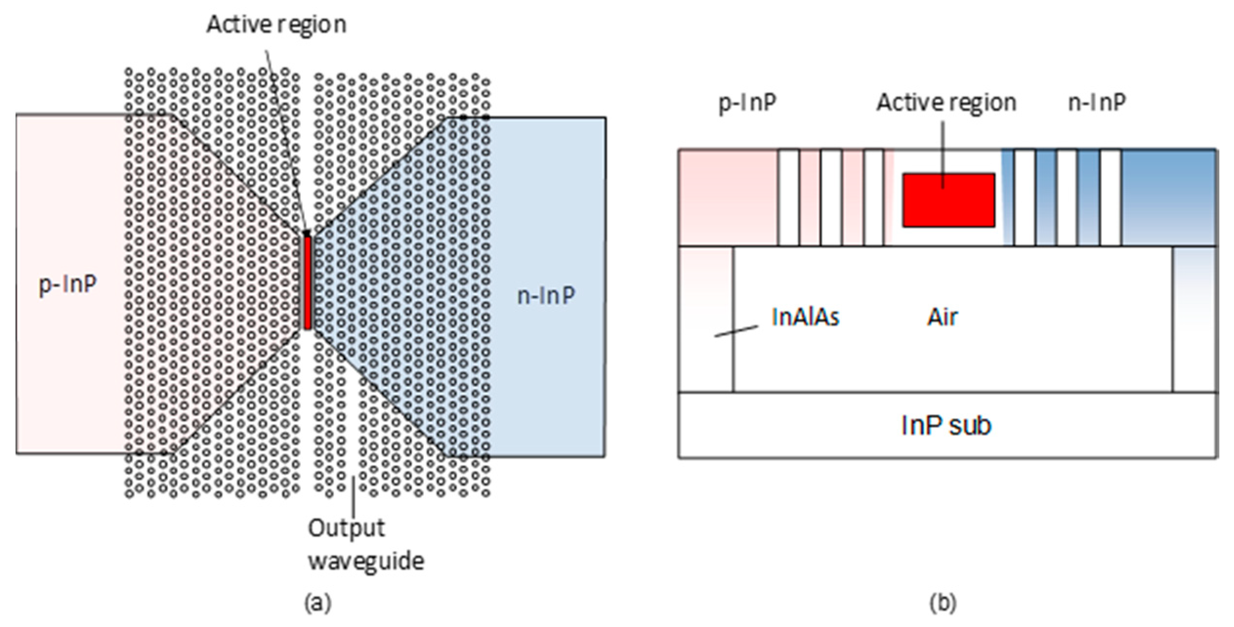
Figure 1 shows the schematics of our PhC laser, in which the wavelength-scale active region is buried in an InP-based PhC line-defect waveguide [10,11,12]. We call this laser a λ-scale embedded active region PhC (LEAP) laser. We use a lateral current injection structure, which is suitable for suppressing the degradation of the cavity Q-factor. For constructing an air bridge structure by selective wet chemical etching, the InAlAs layer is used as a sacrificial layer. As a result, the active region must be entirely covered with an InP layer to protect it from the wet etchant. Since the refractive index of the active region is slightly higher than that of InP, an optical cavity is created around the active region without shifting the positions of the air holes. In addition, the energy bandgap of InP is larger than that of the active region. Typically, the effective refractive indices of the InGaAsP-based active region and the InP layer are 2.77 and 2.59, respectively. Therefore, a BH in a line-defect waveguide provides good confinement for both carriers and photons, which is important for achieving high efficiency. Furthermore, the InP layer, owing to its large thermal conductivity compared with the quaternary gain media, plays a key role in reducing the temperature increase of the active region when heat is generated through current injection. Thanks to these advantages, we have achieved an extremely low threshold input pump power of 1.5 μW, high output power of 100 μW, and 20 Gbit/s direct modulation by optical pumping [13]. The electrically driven LEAP laser has a 4.8 μA threshold current and 4.4 fJ/bit operating energy for 10 Gbit/s NRZ (non-return-to-zero) signal modulation [14].
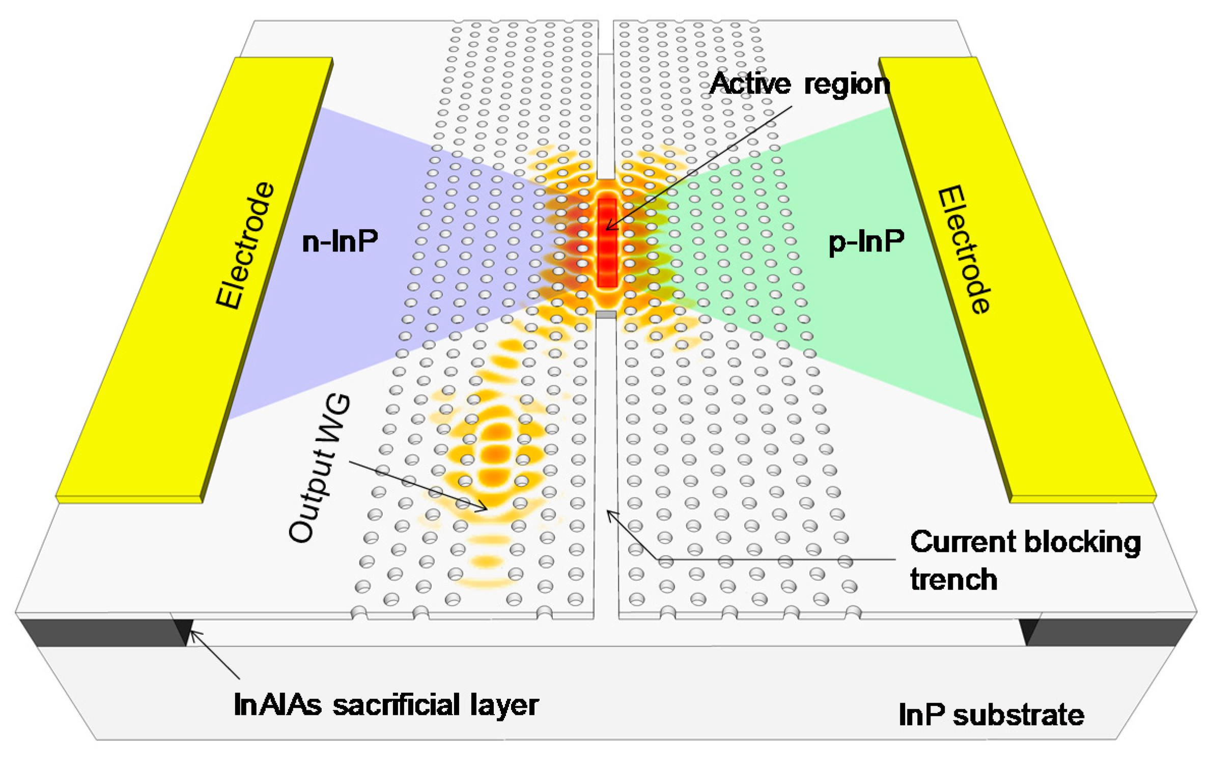
The remaining issues of electrically driven LEAP lasers regard improvements to the wall-plug efficiency and output power. To improve them, we increased the number of QWs and improved the doping process, thereby achieving an output power of 38 μW [15]. However, the threshold current increased to 36 μA due to the leakage current. To solve this problem, we introduced current blocking trenches [14], as shown in Figure 2, which are constructed in the line-defect waveguides. Figure 2 also shows an optical mode, which was calculated by the finite-difference time-domain method. Since the optical mode field of the PhC cavity extends in the Γ–M directions, we can expect a cavity Q-factor of more than 104 even when we construct current blocking trenches.
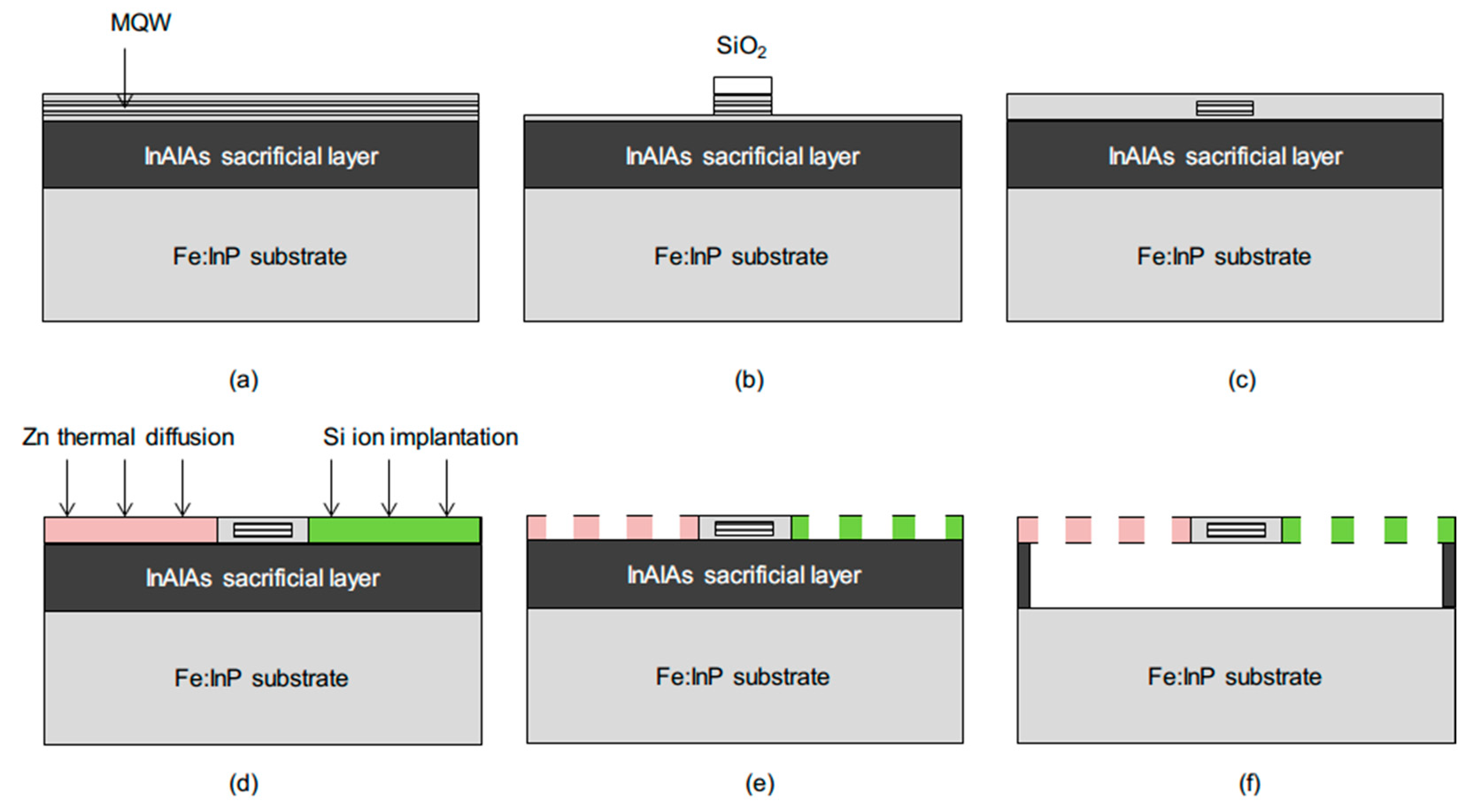
Figure 3 shows the fabrication procedure for an electrically driven LEAP laser. First, we grow an InAlAs sacrificial layer and active region, which is sandwiched by thin InP layers (Figure 3a). A wavelength-scale active region is defined with a SiO2 mask, and the MQW layer, except for the active region, is removed (Figure 3b). Then, the active region is embedded in an InP layer. After the SiO2 mask is removed, a thin InP layer is grown again to obtain a flat top surface (Figure 3c). Si ion implantation and Zn thermal diffusion are used to make n- and p-type doping regions (Figure 3d). Air holes are fabricated by dry etching (Figure 3e), and an air bridge structure is formed by removing the sacrificial layer (Figure 3f). The active region, consisting of six InGaAlAs QWs, was set to 2.5 × 0.3 × 0.15 μm3. The diameter of the PhC holes is 200 nm, and the lattice constant is 420 nm. The InP slab thickness is 250 nm. Current blocking trenches with a width of 200 nm are formed on both longitudinal sides of the BHs.
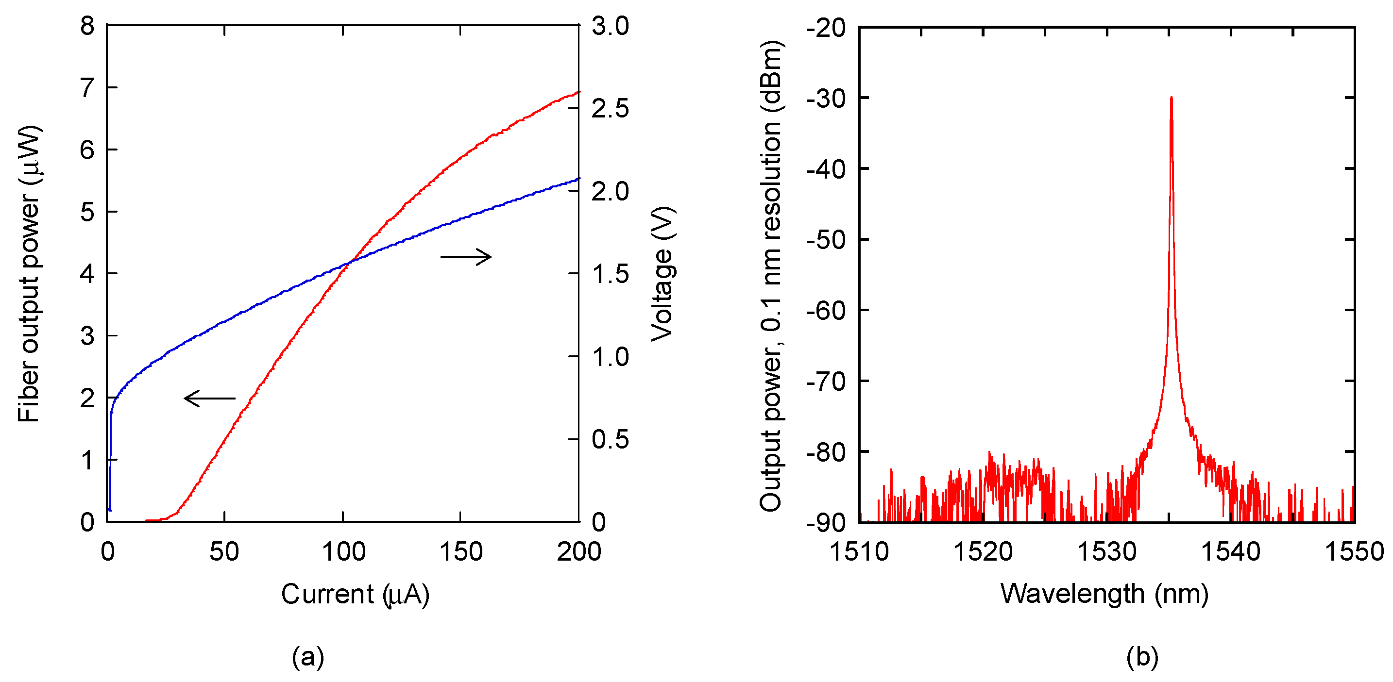
Figure 4a shows the current–light output–voltage (I-L-V) characteristics with RT-CW operation. By employing the current blocking trenches, the threshold current was decreased to 28 μA. The standard single-mode fiber (SSMF) coupled output power was 6.9 μW at a bias current of 200 μA. Thus, estimated output power in the output waveguide (see Figure 2) was 27 μW, when considering the coupling loss between the output waveguide and the SSMF. Since on-board and on-chip interconnects do not need fiber connections, it is very important value and it is enough large to receive the signals by photodetectors. Figure 4b shows the lasing spectrum at a bias current of 100 μA. The lasing wavelength was 1535 nm with a side-mode suppression ratio (SMSR) of 50 dB.
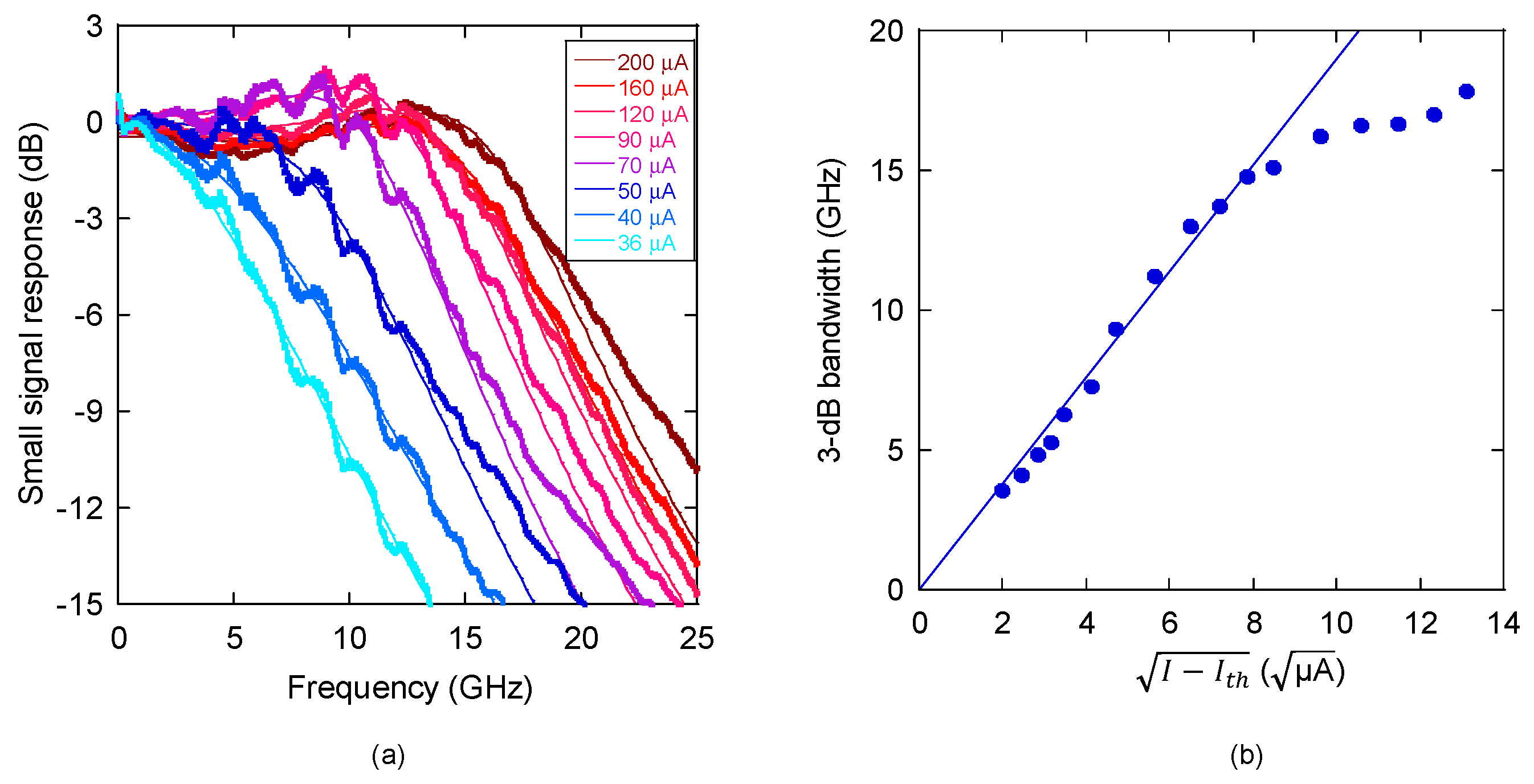
The dynamic responses of the LEAP laser were also measured. Figure 5a shows the measured small-signal responses of the device for various bias currents ranging from 36 to 200 μA. Also shown are fitting curves based on the theoretical curve derived from the laser’s rate equations. The device exhibited a maximum 3 dB bandwidth of 17.8 GHz with an injected current of 200 μA. Figure 5b plots the 3 dB bandwidth versus the square root of the bias current above the threshold. The slope shows the modulation current efficiency (MCEF); we obtained an MCEF of 1.9 GHz/μA0.5, or 60.1 GHz/mA0.5.
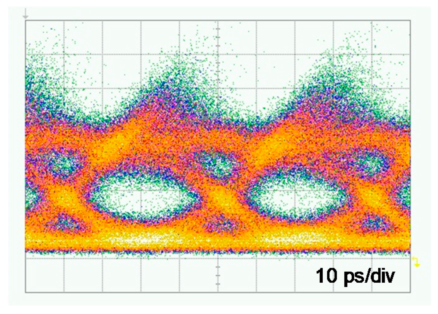
Next, we directly modulated the device with a 25 Gbit/s NRZ signal. Word length of pseudo-random bit sequence (PRBS) was 31. Figure 6 shows the eye diagram measured for a bias current of 150 μA. As shown, we achieved eye opening with 25 Gbit/s NRZ signals. The energy cost was calculated to be 10.5 fJ/bit by dividing the applied DC energy by the bit rate.
3. LEAP Laser on a SiO2/Si Substrate
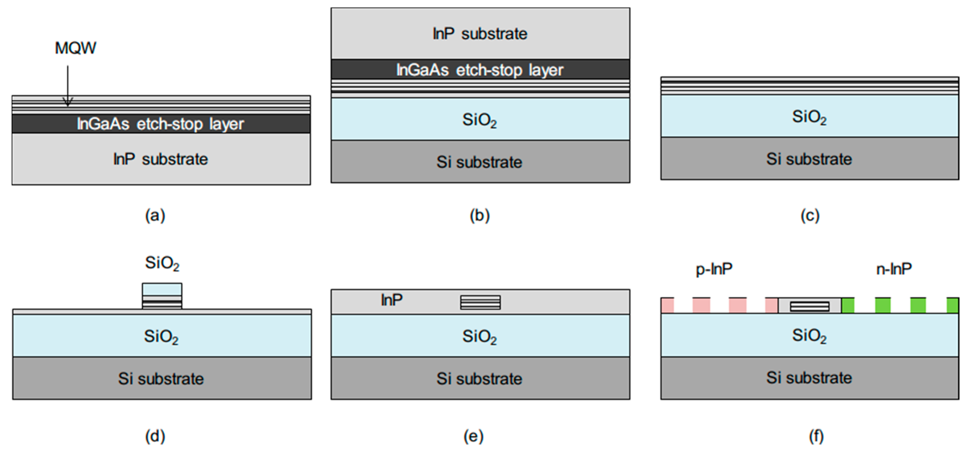
We fabricated a LEAP laser on a SiO2/Si substrate [16,17]. Figure 7 shows the fabrication procedure. First, we grew an InGaAs etch-stop layer and active region, which was sandwiched by thin InP layers, on an InP substrate (Figure 7a). O2-plasma-assisted bonding was used to directly bond epitaxial layers on the SiO2/Si substrate (Figure 7b). Then, the InP substrate and InGaAs layer were selectively etched by chemical etching, after which the active layers remained on the SiO2/Si substrate (Figure 7c). The MQW layers were removed, except for the active region (Figure 7d). We grew an InP layer to bury the active region (Figure 7e). Finally, we fabricated p-and n-doping regions and air holes by using the same fabrication method as described in Figure 3 (Figure 7f). The key factor in achieving epitaxial growth on a thin InP template is the total thickness of the III-V layers, which should be thinner than the critical thickness [18,19]. This fabrication procedure does not require epitaxial growth under lattice-mismatch conditions. However, the different thermal coefficients of Si and InP remain a problem [20,21,22], as it will degrade the crystal quality. In our device configuration, the critical thickness was estimated to be 450 nm [19]. Thus, the use of a lateral current injection structure is quite important. In the future, we will integrate the LEAP laser with a Si waveguide. To make this integration possible, precise positional alignment between the BH and Si waveguide is required. Therefore, the BH should be patterned and formed after wafer bonding because wafer-scale fabrication allows us to make a precise alignment using photolithographical markers on Si.
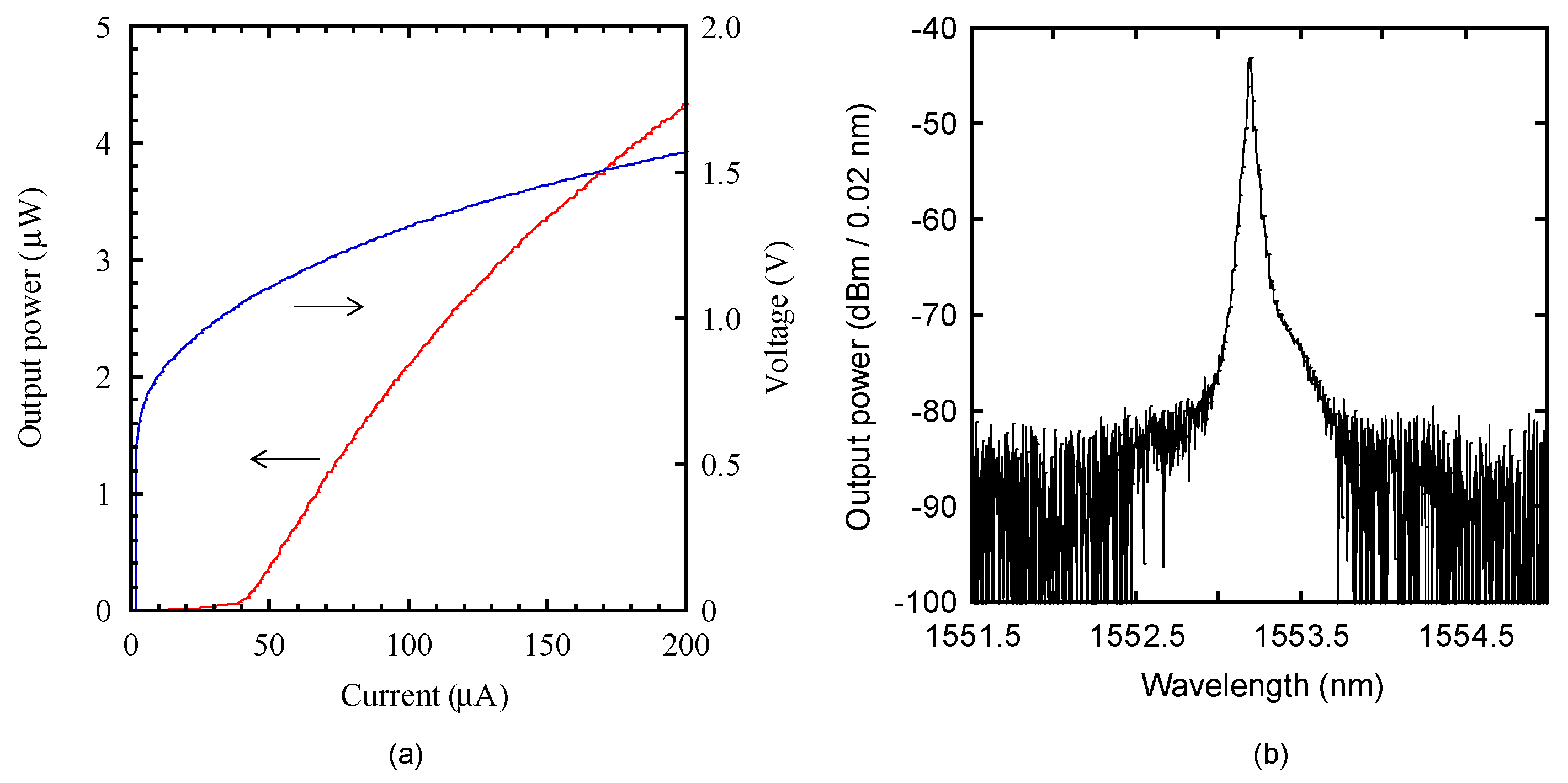
Figure 8a shows the I-L-V characteristics of a fabricated device on a Si substrate in RT-CW operation. The threshold current was 40.5 μA. The maximum output power in the output InP waveguide was 4 μW at a bias current of 200 μA. Figure 8b shows the lasing spectrum at a bias current of 60 μA. Single-mode lasing was achieved at 1553.2 nm.
4. Discussion
As shown in Section 2, we successfully demonstrated high-speed direct modulation with a low operating energy, small enough for use in computercom applications, by using a wavelength-scale cavity. Since the relaxation oscillation frequency fr is proportional to the square root of the carrier density above the threshold, it is important to suppress heat generation to achieve high-speed modulation. This is quite difficult to do for lasers with small active regions because, in general, the laser structures for reducing the active volume are not suitable for current injection. This is because lasers with small active regions must have the same range of cavity Q-factor as conventional lasers with cavity lengths of more than 100 μm. Therefore, a large refractive index difference, typically between those of the semiconductor and air, is required, which results in a high thermal resistance. In this context, employing the BH is the key to the operation of wavelength-scale cavity lasers because InP has a thermal conductivity greater than that of the active material and the energy bandgap difference enables efficient carrier confinement. Furthermore, its strong optical confinement helps to reduce the threshold current and improves the modulation efficiency. By increasing the number of QWs, we can increase the output power and wall-plug efficiency; however, the wall-plug efficiency is still small when compared with conventional in-plane lasers and VCSELs. Here, a further increase in the number of QWs would improve injection efficiency. In addition, the distance and the number of air holes between the active region and the electrodes must be reduced in order to lower the series resistance of the device.
We achieved RT-CW operation with LEAP lasers on a Si substrate, which is promising for integrating them with compact Si photonic devices. On the other hand, the device characteristics were degraded in terms of the threshold current and output power. We believe there are current leakage paths at the interfaces between the InP and SiO2. Therefore, we have to optimize the interface materials and direct bonding fabrication. Furthermore, as shown in [17], the FWHM at threshold was increased compared with that of a device on an InP substrate (air bridge structure). This means we need to further optimize the design of the PhC cavity embedded in the SiO2 layer.
Integration of Si photonic devices will open new application areas for PhC nanodevices, or PICs, for optical computing in deep learning, neuromorphic computing, and so on. This is because such computing requires sophisticated optical circuits based on Mach–Zehnder interferometers which are integrated with low-power-consumption PhC devices made with III-V materials, such as lasers, switches, and nonlinear components.
Recently, we successfully demonstrated the fabrication of a LEAP laser in which the active region is a single lattice constant (~420 nm) [23]. By expanding this, we can fabricate periodic buried active regions, which will enable us to improve the device performance by introducing interesting phenomena such as parity-time (PT) symmetry [24].
5. Conclusions
We obtained a small-signal 3 dB bandwidth of 17.8 GHz and an eye diagram at 25 Gbit/s, thanks to using a combination of a 6 QW wavelength-scale active region and a p-i-n junction position optimized for the BH. The use of a current blocking trench suppressed the leakage current and resulted in a threshold current of 28 μA. The energy consumption of the LEAP laser was as low as 10.5 fJ/bit even when we drove it at 25 Gbit/s with a bias current of 150 μA. These results show that a LEAP laser is suitable as a light source for interconnects on boards and chips. We also demonstrated heterogeneous integration of LEAP lasers on a SiO2/Si substrate. The threshold current was 40.5 μA, and the maximum output power in the output InP waveguide was 4 μW at a bias current of 200 μA. These results are promising for constructing computercom networks using LEAP lasers.
Author Contributions
S.M. supervised the project and wrote the manuscript. K.T. designed and fabricated the devices. K.T. and S.M. performed the measurements.
Acknowledgments
The authors thank Tomonari Sato, Hidetaka Nishi, Koichi Hasebe, Takuro Fujii, Erina Kanno, Masaya Notomi, Akihiko Shinya, Eiichi Kuramochi, Kengo Nozaki, Tai Tsuchizawa, and Hiroshi Fukuda for helpful discussions. We also thank K. Ishibashi, Y. Shouji, and Y. Yokoyama for assistance with the device fabrication.
Conflicts of Interest
The authors declare no conflict of interest.
References
- Miller, D.A.B. Device Requirements for Optical Interconnects to Silicon Chips. Proc. IEEE 2009, 97, 1166–1185. [Google Scholar] [CrossRef] [Green Version]
- Krishnamoorthy, A.; Goossen, K.; Jan, W.; Zheng, X.; Ho, R.; Li, G.; Rozier, R.; Liu, F.; Patil, D.; Lexau, J.; et al. Progress in Low-Power Switched Optical Interconnects. IEEE J. Sel. Top. Quantum Electron. 2011, 17, 357–376. [Google Scholar] [CrossRef]
- Moser, P.; Lott, J.A.; Wolf, P.; Larisch, G.; Li, H.; Ledentsov, N.N.; Bimberg, D. 56 fJ dissipated energy per bit of oxide-confined 850 nm VCSELs operating at 25 Gbit/s. Electron. Lett. 2012, 48, 1292–1294. [Google Scholar] [CrossRef]
- Li, H.; Wolf, P.; Moser, P.; Larisch, G.; Mutig, A.; Lott, J.A. Bimberg Energy-efficient and temperature-stable oxide-confined 980 nm VCSELs operating error-free at 38 Gbit/s at 85 °C. Electron. Lett. 2014, 50, 103–105. [Google Scholar] [CrossRef]
- Matsuo, S.; Sato, T.; Takeda, K.; Shinya, A.; Nozaki, K.; Kuramochi, E.; Taniyama, H.; Notomi, M.; Fujii, T.; Hasebe, K.; et al. Photonic crystal lasers using wavelength-scale embedded active region. J. Phys. D 2014, 47, 023001. [Google Scholar] [CrossRef]
- Matsuo, S.; Kakitsuka, T. Low-operating-energy directly modulated lasers for short-distance optical interconnects. Adv. Opt. Photon. 2018, 10, 567–643. [Google Scholar] [CrossRef]
- Tanabe, T.; Notomi, M.; Kuramochi, E.; Shinya, A.; Taniyama, H. Trapping and delaying photons for one nanosecond in an ultrasmall high-Q photonic-crystal nanocavity. Nat. Photon. 2007, 1, 49–52. [Google Scholar] [CrossRef]
- Takahashi, Y.; Hagino, H.; Tanaka, Y.; Song, B.-S.; Asano, T.; Noda, S. High-Q nanocavity with a 2-ns photon lifetime. Opt. Express 2007, 15, 17206–17213. [Google Scholar] [CrossRef]
- Painter, O.; Lee, R.K.; Scherer, A.; Yariv, A.; O’Brien, J.D.; Dapkus, P.D.; Kim, I. Two-Dimensional Photonic Band-Gap Defect Mode Laser. Science 1999, 284, 1819–1821. [Google Scholar] [CrossRef] [Green Version]
- Matsuo, S.; Shinya, A.; Kakitsuka, T.; Nozaki, K.; Segawa, T.; Sato, T.; Kawaguchi, Y.; Notomi, M. High-speed ultracompact buried heterostructure photonic-crystal laser with 13 fJ of energy consumed per bit transmitted. Nat. Photon. 2010, 4, 648–654. [Google Scholar] [CrossRef]
- Matsuo, S.; Shinya, A.; Kakitsuka, T.; Nozaki, K.; Segawa, T.; Sato, T.; Kawaguchi, Y.; Notomi, M. Room-temperature continuous-wave operation of lateral current injection wavelength-scale embedded active-region photonic-crystal laser. Opt. Express 2012, 20, 3773–3780. [Google Scholar] [CrossRef] [PubMed]
- Matsuo, S.; Sato, T.; Takeda, K.; Shinya, A.; Nozaki, K.; Taniyama, H.; Notomi, M.; Hasebe, K.; Kakitsuka, T. Ultra-low operating energy electrically driven photonic crystal lasers. IEEE J. Sel. Top. Quantum Electron. 2013, 19, 4900311. [Google Scholar] [CrossRef]
- Matsuo, S.; Shinya, A.; Chen, C.-H.; Nozaki, K.; Sato, T.; Kawaguchi, Y.; Taniyama, H.; Notomi, M. 20-Gbit/s directly modulated photonic crystal nanocavity laser with ultra-low power consumption. Opt. Express 2011, 19, 2242–2250. [Google Scholar] [CrossRef] [PubMed]
- Takeda, K.; Sato, T.; Shinya, A.; Nozaki, K.; Kobayashi, W.; Taniyama, H.; Notomi, M.; Hasebe, K.; Kakitsuka, T.; Matsuo, M. Few-fJ/bit data transmissions using directly modulated lambda-scale embedded active region photonic-crystal lasers. Nat. Photon. 2013, 7, 569–575. [Google Scholar] [CrossRef]
- Sato, T.; Takeda, K.; Shinya, A.; Notomi, M.; Hasebe, K.; Kakitsuka, T.; Matsuo, M. Photonic Crystal Lasers for Chip-to-Chip and On-Chip Optical Interconnects. IEEE J. Sel. Top. Quantum Electron. 2015, 21, 4900410. [Google Scholar] [CrossRef]
- Takeda, K.; Sato, T.; Fujii, T.; Kuramochi, E.; Notomi, M.; Hasebe, K.; Kakitsuka, T.; Matsuo, M. Heterogeneously integrated photonic-crystal lasers on silicon for on/off chip optical interconnects. Opt. Express 2015, 23, 702–708. [Google Scholar] [CrossRef] [PubMed]
- Takeda, K.; Fujii, T.; Shinya, A.; Kuramochi, E.; Notomi, M.; Hasebe, K.; Kakitsuka, T.; Matsuo, M. Photonic-crystal lasers on silicon for chip-scale optical interconnects. Proc. SPIE Photon. West 2016, 9767, 976710. [Google Scholar]
- Matsuo, M.; Fujii, T.; Hasebe, K.; Takeda, K.; Sato, T.; Kakitsuka, T. Directly modulated buried heterostructure DFB laser on SiO2/Si substrate fabricated by regrowth of InP using bonded active layer. Opt. Express 2014, 22, 12139–12147. [Google Scholar] [CrossRef]
- Fujii, T.; Sato, T.; Takeda, K.; Hasebe, K.; Kakitsuka, T.; Matsuo, M. Epitaxial growth of InP to bury directly bonded thin active layer on SiO2/Si substrate for fabricating distributed feedback lasers on silicon. IET Optoelectron. 2015, 9, 151–157. [Google Scholar] [CrossRef]
- Fontcubertai Morral, A.; Zahler, J.M.; Atwater, H.A. InGaAs/InP double heterostructures on InP/Si templates fabricated by wafer bonding and hydrogen-induced exfoliation. Appl. Phys. Lett. 2003, 83, 5413–5415. [Google Scholar] [CrossRef] [Green Version]
- Zhang, C.; Liang, D.; Bowers, J.E. MOCVD regrowth of InP on hybrid silicon substrate. ECS Solid State Lett. 2013, 2, Q82–Q86. [Google Scholar] [CrossRef]
- Matsumoto, K.; Makino, T.; Kimura, K.; Shimomura, K. Growth of GaInAs/InP MQW using MOVPE on directly-bonded InP/Si substrate. J. Cryst. Growth 2013, 370, 133–135. [Google Scholar] [CrossRef]
- Takeda, K.; Fujii, T.; Kuramochi, E.; Shinya, A.; Notomi, K.; Kakitsuka, T.; Matsuo, M. Reduction of Cavity Length in λ-scale Embedded Active-region Photonic Crystal (LEAP) Lasers. In Proceedings of the 2018 IEEE International Semiconductor Laser Conference (ISLC), Santa Fe, NM, USA, 16–19 September 2018; pp. 103–104. [Google Scholar]
- Takata, K.; Notomi, M. Photonic Topological Insulating Phase Induced Solely by Gain and Loss. Phys. Rev. Lett. 2018, 121, 213902. [Google Scholar] [CrossRef] [PubMed] [Green Version]
Figure 1.
Schematics of the λ-scale embedded active region photonic crystal (LEAP) laser: (a) top view; (b) cross-sectional view. The wavelength-scale active region is embedded in a line-defect waveguide of InP-based photonic crystal (PhC). Since the refractive index of the active region is slightly higher than that of InP, an optical cavity is created around the active region without shifting the positions of the air holes. Typically, the effective refractive indices of the InGaAsP-based active region and the InP layer are 2.77 and 2.59, respectively.

Figure 2.
Schematic of a fabricated LEAP laser with a current blocking trench. An optical mode, calculated by the finite-difference time-domain method, is overwritten on the schematic.
Figure 2.
Schematic of a fabricated LEAP laser with a current blocking trench. An optical mode, calculated by the finite-difference time-domain method, is overwritten on the schematic.

Figure 3.
Fabrication of a LEAP laser: (a) Epitaxial growth of the active layer; (b) removal of multiple quantum wells (MQW), except for the active region; (c) buried regrowth; (d) p-and n-type doping; (e) air hole fabrication; (f) air bridge structure formation by sacrificial layer etching.
Figure 3.
Fabrication of a LEAP laser: (a) Epitaxial growth of the active layer; (b) removal of multiple quantum wells (MQW), except for the active region; (c) buried regrowth; (d) p-and n-type doping; (e) air hole fabrication; (f) air bridge structure formation by sacrificial layer etching.

Figure 4.
Static characteristics of a LEAP laser on InP substrate: (a) current–light output (red) and current–voltage (blue) characteristics under room-temperature continuous-wave (RT-CW) conditions; (b) lasing spectrum at a bias current of 100 μA.
Figure 4.
Static characteristics of a LEAP laser on InP substrate: (a) current–light output (red) and current–voltage (blue) characteristics under room-temperature continuous-wave (RT-CW) conditions; (b) lasing spectrum at a bias current of 100 μA.

Figure 5.
(a) Small-signal responses of the device for various bias currents ranging from 36 to 200 μA. Fitting curves based on rate equations are also shown. (b) 3 dB bandwidth versus the square root of the bias current above the threshold.
Figure 5.
(a) Small-signal responses of the device for various bias currents ranging from 36 to 200 μA. Fitting curves based on rate equations are also shown. (b) 3 dB bandwidth versus the square root of the bias current above the threshold.

Figure 6.
Eye diagram of the LEAP laser for a 25 Gbit/s NRZ signal. Bias current was 150 μA.

Figure 7.
Fabrication procedure for a LEAP laser on Si: (a) epitaxial growth of the active layer; (b) direct bonding of the InP substrate including the active layer and SiO2/Si substrate; (c) removal of the InP substrate and sacrificial layer; (d) removal of the active layer except for the active region; (e) buried regrowth; (f) selective doping and air hole fabrication.

Figure 8.
(a) I-L-V characteristics under RT-CW operation. (b) Lasing spectrum at bias current of 60 μA.
Figure 8.
(a) I-L-V characteristics under RT-CW operation. (b) Lasing spectrum at bias current of 60 μA.

© 2019 by the authors. Licensee MDPI, Basel, Switzerland. This article is an open access article distributed under the terms and conditions of the Creative Commons Attribution (CC BY) license (http://creativecommons.org/licenses/by/4.0/).
Share and Cite
MDPI and ACS Style
Matsuo, S.; Takeda, K. λ-Scale Embedded Active Region Photonic Crystal (LEAP) Lasers for Optical Interconnects. Photonics 2019, 6, 82. https://doi.org/10.3390/photonics6030082
AMA Style
Matsuo S, Takeda K. λ-Scale Embedded Active Region Photonic Crystal (LEAP) Lasers for Optical Interconnects. Photonics. 2019; 6(3):82. https://doi.org/10.3390/photonics6030082
Chicago/Turabian StyleMatsuo, Shinji, and Koji Takeda. 2019. "λ-Scale Embedded Active Region Photonic Crystal (LEAP) Lasers for Optical Interconnects" Photonics 6, no. 3: 82. https://doi.org/10.3390/photonics6030082
Note that from the first issue of 2016, this journal uses article numbers instead of page numbers. See further details here.