Fabrication of Cu2ZnSnS4 Thin Films from Ball-Milled Nanoparticle inks under Various Annealing Temperatures


1
Zhongshan Institute, University of Electronic Science and Technology of China, Zhongshan 528402, China
2
PANOTECH. INC. 7-13-6 Ginza, Tyouo-Ku, Toyo 1040061, Japan
3
State Key Laboratory of Nuclear Physics and Technology, School of Physics, Peking University, Beijing 100871, China
4
Guangdong Engineering-Technology Research Center of Nano-Photoelectric Functional Films and Devices, Zhongshan 528402, China
*
Authors to whom correspondence should be addressed.
Nanomaterials 2019, 9(11), 1615; https://doi.org/10.3390/nano9111615
Submission received: 28 September 2019
/
Revised: 4 November 2019
/
Accepted: 8 November 2019
/
Published: 14 November 2019
Abstract
:Cu2ZnSnS4 (CZTS) has been recognized as a promising thin-film absorber material of chalcopyrite-related solar cells. A two-stage method for fabricating CZTS films using CZTS nanoparticles was developed. Nanocrystal inks fabricated by a ball-milling method was utilized to °C deposit CZTS precursors by spin-coating approach. The CZTS precursors were annealed in the sulfur atmosphere under different annealing temperatures ranging from 550 °C to 650 °C. Influences of annealing temperature on grain growth, composition, crystallinity, and photovoltaic properties of CZTS films were characterized. With the increase of annealing temperature, grain growth was enhanced, while the sulfur atomic ratio fist increased then decreased. The crystallinity of the films was significantly improved after the annealing, and the obvious peak of the secondary phase of ZnS, were observed from the X-ray diffraction results, when the annealing temperature increased to 625 °C. However, the secondary phase was not detected from the surface Raman spectrum. Through comparing the Raman spectrum of different areas of the CZTS film, secondary phases of ZnS and SnS were observed, indicating the decomposition of CZTS films, due to the high temperature. The highest conversion efficiency of 7.5% was obtained when the annealing temperature was 600 °C.
1. Introduction
The quaternary semiconductor Cu2ZnSnS4 (CZTS) using just earth-abundant materials and its counterpart Cu2ZnSn(S, Se)4 (CZTSSe), in which some of the sulfur atoms are replaced by selenium, are very promising thin film photovoltaic absorber layers of solar cell in the future, due to the ideal optical properties, nontoxicity, and low cost of the constituent elements [1,2,3]. 1.5 eV bandgap of the pure CZTS is nearly ideal for single-junction solar cell, and the bandgap can be tuned to less than 1.0 eV by substituting the sulfur atoms by selenium atoms [4]. Due to this merit, CZTS-based devices are expected to have the same theoretical efficiency as Cu(In, Ga)Se2 (CIGS) solar cell [5]. Although, up to now efficiency of pure CZTS solar cell has surpassed 10%, while CZTSSe solar cell has achieved a record efficiency of 12.6% by a typical hydrazine-solution based synthesis method recently [6]. However, utilization of hydrazine has limited the popularization because of the toxicity and residual of organic solvents in the film [7]. As a result, alternative solution process route using just non-toxic solvents have been reported by several groups [8,9,10].
In this work, we report our unique approach for fabricating CZTS films by a so-called ‘two-stage’ method from the CZTS nanocrystal inks, that is, CZTS nanoparticles are firstly deposited on the substrate by a spin-coating method to obtain CZTS precursor. The as-deposited precursors are then annealed in the sulfur atmosphere at a high temperature to get large grain size and better crystallinity. Specific details have been revealed in our previous publications [11,12]. It has been reported that the following reaction could move forward or reverse, depending on the annealing temperature and sulfur vapor pressure [13,14]:
In our case, sulfur vapor pressure is also controlled by the annealing temperature. As a result, annealing temperature plays a very important role in the two-stage process. In this paper, our aim is to study the influence of annealing temperature on the properties of CZTS films. Dependence of the morphology, composition, crystallinity, and electrical properties on annealing temperature is investigated.
2. Experimental Method
CZTS source powder with 99.999% purity was obtained from High Purity Materials Kojundo Chemical Laboratory Co., Ltd. (Saitama, Japan). CZTS nanocrystal inks were fabricated by ball-milling method, which have been discussed in detail, in our previous work [11]. The CZTS precursor was then deposited on the glass substrate using the as-fabricated inks by a spin-coating approach. The precursor and elemental sulfur powder (99.999%) were placed in an ampoule, which was evacuated to around 2.0 × 10⁻³ Pa, and N2 gas (99.99%) was used to fill the ampoule to get a final pressure of around 2.0 × 10⁻⁴ Pa. Then the ampoule was sealed up to isolate the substrate and sulfur with the surrounding. The annealing was conducted in a cubic annealing furnace with a temperature deviation from the setting value of less than 1% in the atmosphere. N2 gas was used as the carrier of heat to enhance heat exchange between the substrate and the furnace and to adjust the partial pressure of sulfur. The total pressure in the ampoule was adjusted to less than 1.0 × 10⁻⁵ Pa atm during the annealing process by presetting the pressure of N2. The annealing temperature was selected between 550 °C and 650 °C with an interval of 25 °C for each sample, and, in total, five temperatures were conducted. The annealing furnace was set at a heating rate from room temperature to the target temperature of 15 °C min−1. The total annealing time was chosen to be 3 h. After the annealing was finished, the ampoule was cold together with the furnace naturally to around 400 °C to provide the substrate with sulfur atmosphere protection, since lack of sulfur vapor will lead to decomposition of CZTS films at a high temperature, of over 400 °C, judging from reaction (1). Then the ampoule was withdrawn to the atmosphere, cooling down to less than 200 °C within 5 min to get rid of sulfur condensation on the surface of CZTS film. Comparing with Reference [11], experimental parameters in this work were greatly different. Firstly, in Reference [11], it was a rapid annealing process, during which the increasing rate of annealing temperature was 40 °C min−1, while in this work, it was 15 °C min−1. Rapid temperature increase could generate temperature nonuniformity, leading to ununiform annealing result. Secondly, the annealing process at 600 °C lasted for 20 min in Reference [11]. In this work, it was 3 h. The raised annealing temperature can promote crystallization and grain growth of CZTS films. Finally, in this work, the ampoule was filled with N2, which promoted heat transmission and ensured the sample temperature is the same with setting temperature. In Reference [11], the ampoule was set with high vacuum, and heat transmission was dominated by radiation. Together with the short annealing time, it makes temperature of the substrate deviated from the setting value. Thus, the annealing result could be different for the two works.
Then, the as-grown CZTS film was taken out of the ampoule and used to conduct characterization immediately. To check photovoltaic properties of CZTS films, the full solar cell structure was completed, as follows: A 50-nm-thick CdS buffer layer was first deposited on CZTS film by chemical bath deposition; then layers of metal-organic chemical vapor deposited i-ZnO (80 nm) and B-doped ZnO (600 nm). Finally, a front-contact Al grid was deposited on the top via evaporation method.
The morphology of the CZTS films was characterized with a scanning electron microscope (SEM) equipped with a JED-2300T energy dispersive spectroscopy (EDS) system (JSM-7001F, JEOL, Tokyo, Japan) operating at an acceleration voltage of 10 kV. EDS was measured at an acceleration voltage of 15 kV for compositional analysis. Crystallization of CZTS film was performed by X-ray diffraction (XRD) (SmartLab, Rigaku Corporation, Tokyo, Japan) with a voltage of 40 kV and 20 mA current. Raman spectra was measured by a Raman spectrometer (RS-1000, JASCO Corporation, Tokyo, Japan) with a resolution of 1.6 cm−1. Solar cell performance was measured with a 913 CV type current-voltage (J-V) tester (AM1.5) provided by a solar simulator (LP-50B, EKO, Tokyo, Japan). The simulator was calibrated by a standard GaAs solar cell to get the standard illumination density (100 mW/cm−2). Quantum efficiency (QE) of CZTS solar cell was characterized by a QE tester (QE-2000, Otsuka Electronics Co., Ltd., Osaka, Japan).
3. Results and Discussions
3.1. Surface and Cross-Sectional SEM
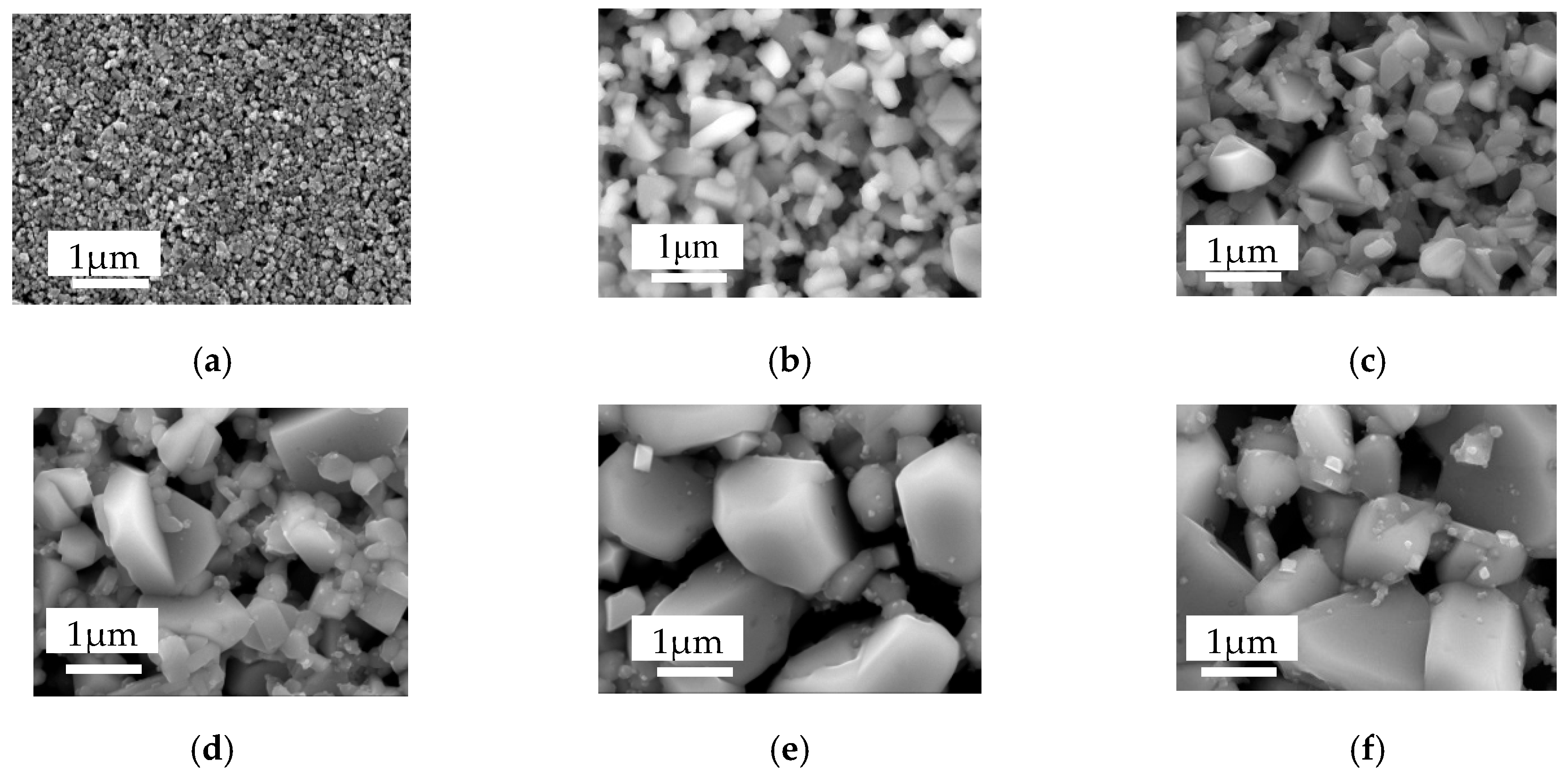
Surface SEM micrographs of the CZTS precursor and some of the annealed films are shown in Figure 1. The precursor shows a very small grain size of several-ten nm, as shown in Figure 1a. After the precursor being annealed under a temperature of 550 °C (Figure 1b) the grain size significantly increases. The whole film morphology can be described as large grains up to 1 μm embed in the small grains of several-hundred nm. With increasing annealing temperature from 550–650 °C the grain size increased gradually. The basic morphology for annealing temperature 550–600 °C (Figure 1b–d) are identical; however, when the temperature is raised to 625 °C the large grains over 1 μm begin to dominate, accompanied by a small number of small size grains (Figure 1e). Grains continue to increase over 2 μm as the temperature is increased to 650 °C (Figure 1f). Cross-sectional SEM micrographs of the annealed films with different annealing temperatures are shown in Figure 2. Cross-sectional image for precursor is absent because it is difficult to prepare appropriate SEM sample, due to the low combining power between the particles. (When one breaks off the substrate, the fresh cross-section is too rough to be observed by SEM). As can be seen from the figures, with the increase of annealing temperatures, the grain size of CZTS films increases significantly, especially when the temperature is over 625 °C large grain of over 2 μm dominates, which is consistent with the surface SEM results. However, pinholes stretching throughout the film in the thickness direction begin to show up, meaning deterioration of the film quality, due to the film decomposition.
3.2. Composition of CZTS Films
Table 1 shows composition of CZTS films annealed with different temperature. The precursor shows a sulfur and zinc poor composition comparing to the high quality CZTS films reported by other groups [15,16]. After the film is annealed at a nominal temperature of 550 °C in our case, the composition becomes sulfur-rich, and when the annealing temperature is increased to 575 °C, the sulfur ratio continues to increase. However, when the temperature is further increased, the sulfur ratio begins to decrease and get the minimum value of less than 50%. This result can be explained, as follows: There is a balance between the absorption and emission of sulfur during the annealing process related to the sulfur pressure and substrate temperature. When the annealing temperature increases, sulfur vapor pressure increases as well, which promote the absorption of elemental sulfur. However, when the substrate temperature goes over 600 °C, the emission of sulfur is significantly enhanced; leading to sulfur loss and sulfur-poor composition. Meanwhile, the Sn ratio varies a little even the temperature ranges up to 650 °C, indicating low loss of tin.
3.3. X-ray Diffraction and Raman Scattering Spectra Characterization
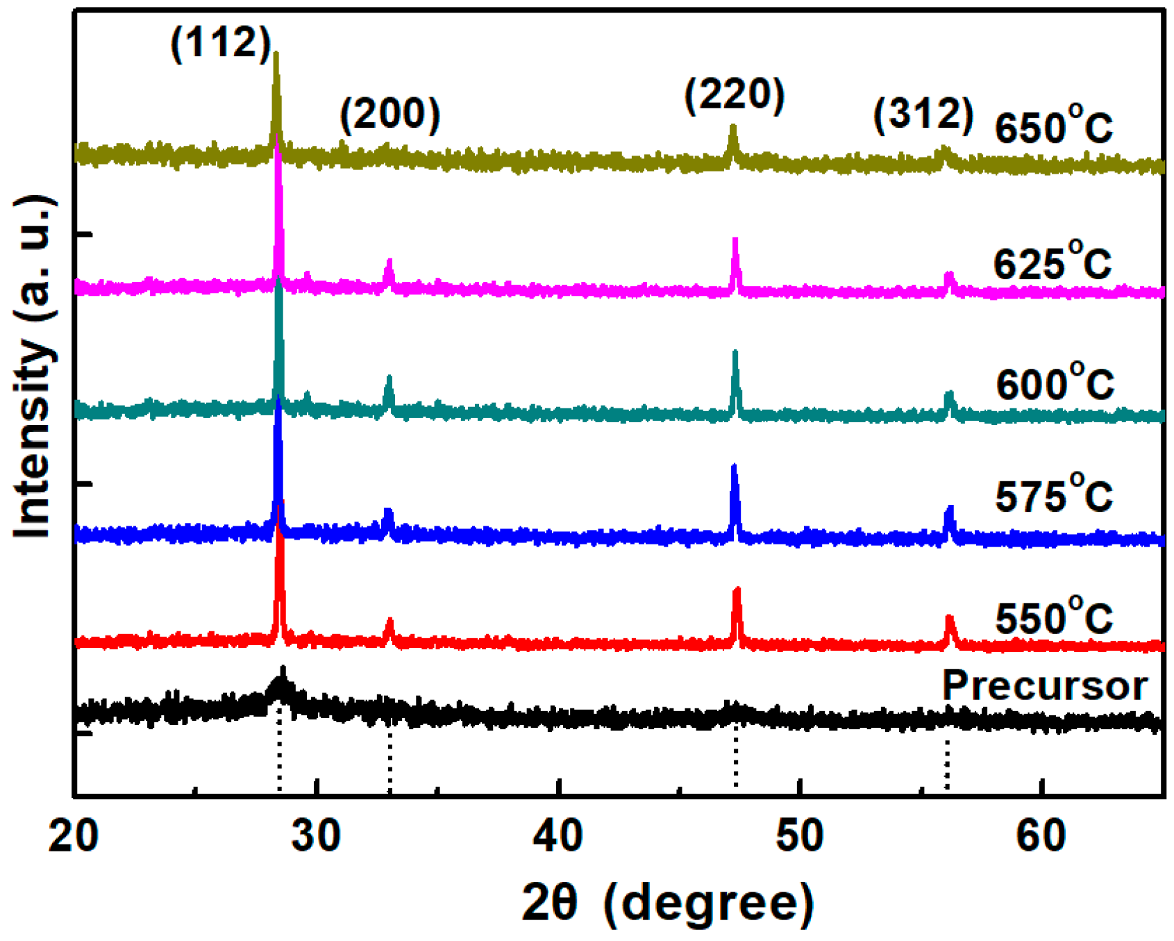
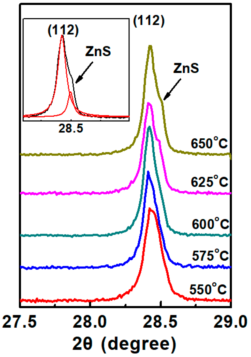
XRD patterns of CZTS films are shown in Figure 3. The phase identification pointed to the presence of kesterite structural CZTS films according to Reference [17]. The precursor shows very weak diffraction peaks and just one broad peak around 2θ = 28.5° can be observed, indicating low crystallinity. The 550 °C annealed CZTS film exhibits four peaks at 2θ = 28.5°, 33.0°, 47.3° and 56.5°, corresponding to the peaks of (112), (200), (220) and (321) of kesterite phase CZTS structure, respectively. When the annealing temperature increases, the intensity of the diffraction peaks also increases and gets the maximum value when the annealing temperature is 600 °C, meaning the improvement of the crystallinity. For 625 °C and 650 °C annealed films, the peak intensity slightly decreased, which can be explained by Figure 4 that shows the XRD pattern of (112) plane of annealed CZTS films with different annealing temperatures. For 550 and 575 °C annealed films, the XRD pattern shows a single (112) peak, illustrating no secondary phases can be detected. However, when the annealing temperature is increased to 625 °C, a slight hump begins to show up at the right side of the peak of (112) plane, which is attributed to the peak of ZnS [18], indicating secondary phase. Judging from reaction (1), as has been mentioned above; when the annealing temperature is over 600 °C, the reaction will go the forward direction. The formation of ZnS will generate a correspondent peak in the XRD pattern.
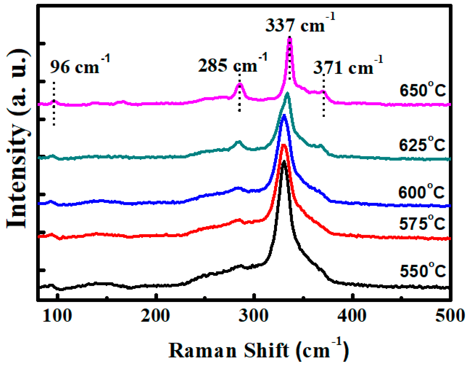
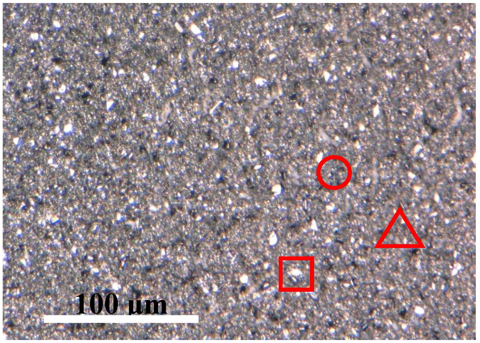
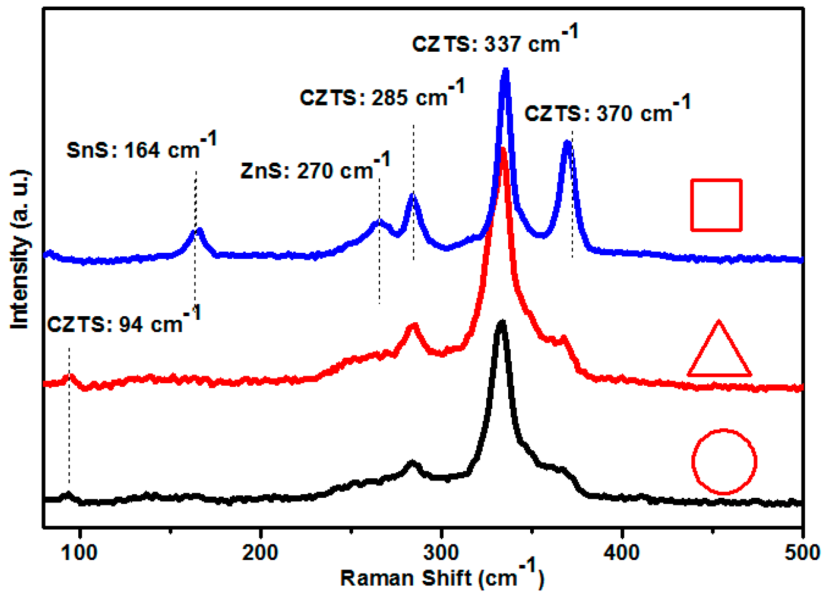
To further clarify the secondary phase, surface Raman scattering measurement was conducted with 532 nm excitation wavelength. Figure 5 shows the Raman scattering spectra of CZTS films with different annealing temperatures. The peaks are marked with correspondent phases. Judging from the Raman result, all the phases can be assigned to kesterite CZTS film. The films exhibit a typical Raman spectrum of kesterite CZTS films. The two main peaks of 285.4 and 337 cm−1 are corresponding to two A modes, and the shoulder at 372 and a minor peak at 96 cm−1 are corresponding to two of the B symmetry modes of the CZTS kesterite structure [19,20,21], respectively. Even though obvious ZnS peak is observed in the XRD spectra, no secondary phases have been detected by the Raman spectrum, although detect of secondary phases for Raman is easier than XRD. A possible explanation is that distribution of secondary phases was ununiform, and the measured area has a small amount. Meanwhile, the spectral resolution was insufficient to distinguish the ZnS peak, which was superimposed by the peaks of CZTS. Figure 6 is a 3D microscope image that illustrates the different areas where Raman measurement has been performed: The circle area is for the normal flat area, the triangle represents flat area mixed with larger particles, and square shows the large particle area. In order to further identify the reason for these results, Raman measurement is conducted on a different area of a CZTS film annealed at 625 °C, as shown in Figure 7. According to the Raman spectrums, only classic peaks of kesterite CZTS film can be observed in the normal flat area. For the marked triangle area, a shoulder of CZTS peak (285 cm−1) appears near 270 cm−1. It is inferred that it belongs to the A1 mode of ZnS [22,23], which is consistent with our XRD result. For the square marked area, besides the peak of 270 cm−1, a minor peak at 164 cm−1 is present, corresponding to the SnS compound [24,25]. The presence of the peaks of ZnS and SnS illustrate the decomposition of CZTS during the high temperature process. However, Cu3SnS4 reported somewhere else [26] was not detected in our samples.
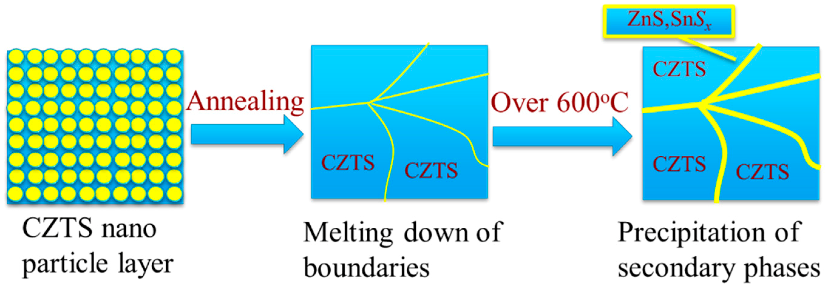
The schematic of the growth mechanism for CZTS films was shown in Figure 8. During the annealing process, with the increase of temperature grain boundaries gradually meltdown, and grain size became larger. Thus, annealing process played a key role in grain growth. However, when the annealing temperature was over 600 °C CZTS crystal started to decompose at the grain boundary, leading to the formation of secondary phases at the boundary and extremely large grains formed, which caused surficial nonuniformity, as shown in Figure 2e,f. Thus, secondary phases, such as ZnS and SnSx were detected when the annealing temperature was 625 °C.
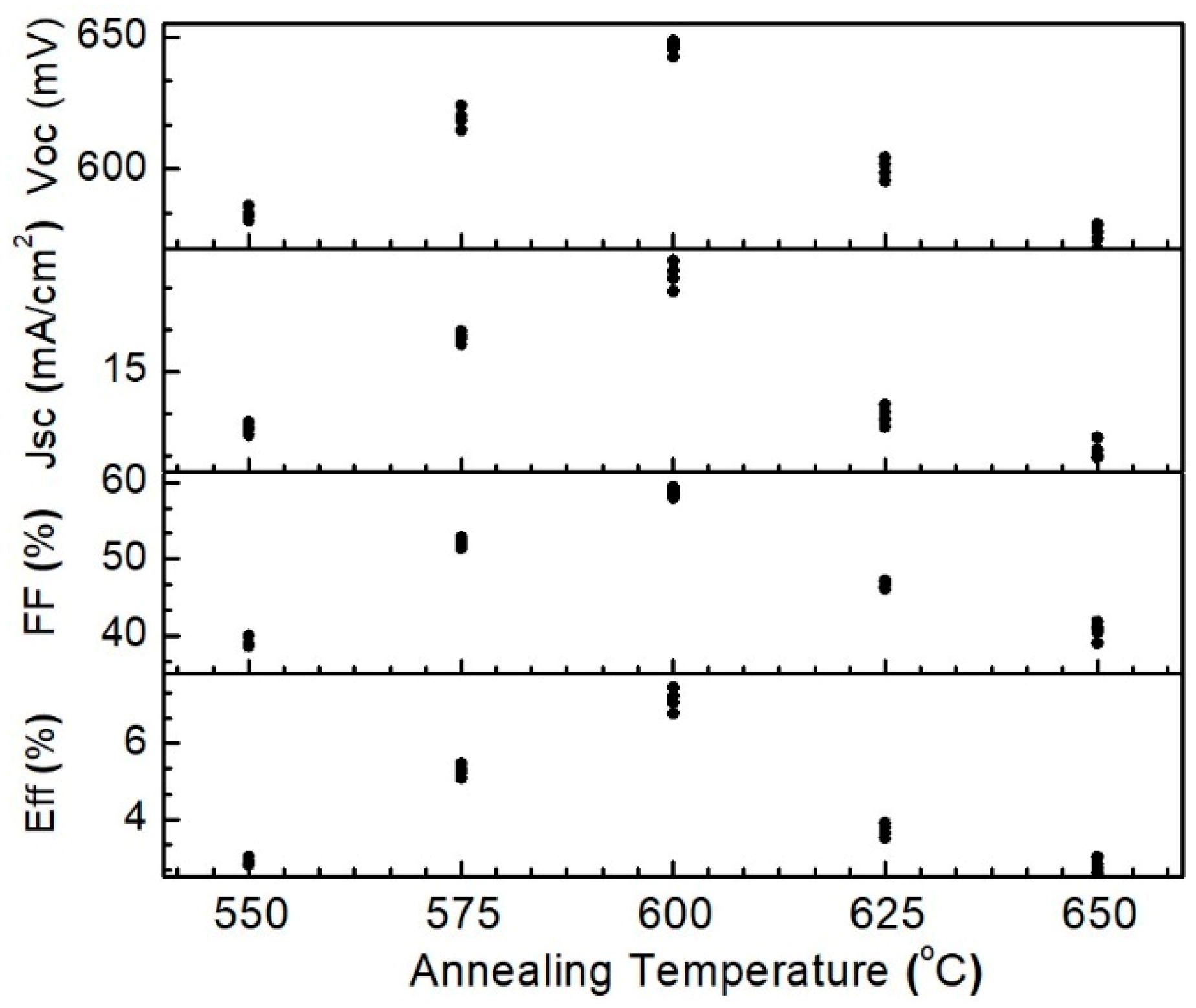
The CZTS films were then fabricated to full solar cell structure, and solar cell performance was evaluated under standard conditions with irradiation of 100 mW/cm2. The intensity of the solar simulator was calibrated by a high-precision monocrystalline Si solar cell to achieve a standard illumination. Figure 9 shows the photovoltaic characteristics of CZTS solar cells annealed at different temperature with an area of 0.2 cm2. Considering of system errors and circumstances of experiment, the measurement was carried on four samples for each annealing temperature. When the annealing temperature was 550 °C, the conversion efficiency of CZTS solar cell is about 2.8%, with a low open-circuit voltage (Voc) of about 586 mV, a short circuit current (Jsc) of 12.5 mA/cm2, and fill factor (FF) of 38.5%. It was inferred that the low performance of the solar cell was due to the low crystallinity of CZTS film because of low annealing temperature. With the increase of annealing temperature, the crystallinity of the absorber layer was improved, which lead to better solar cell performance. The CZTS solar showed a conversion efficiency of around 5.2% (Voc: 618.5 mV, Jsc: 16.3 mA/cm2, FF: 51.9%) and the highest value of 7.5% (Voc: 647 mV, Jsc: 16.3 mA/cm2, FF: 51.9%) was obtained when the annealing temperature was 600 °C. However, when the annealing temperature further increased, solar cell performance began to deteriorate, as shown in the figure. One explanation was the formation of secondary phases because of the decomposition of CZTS films.
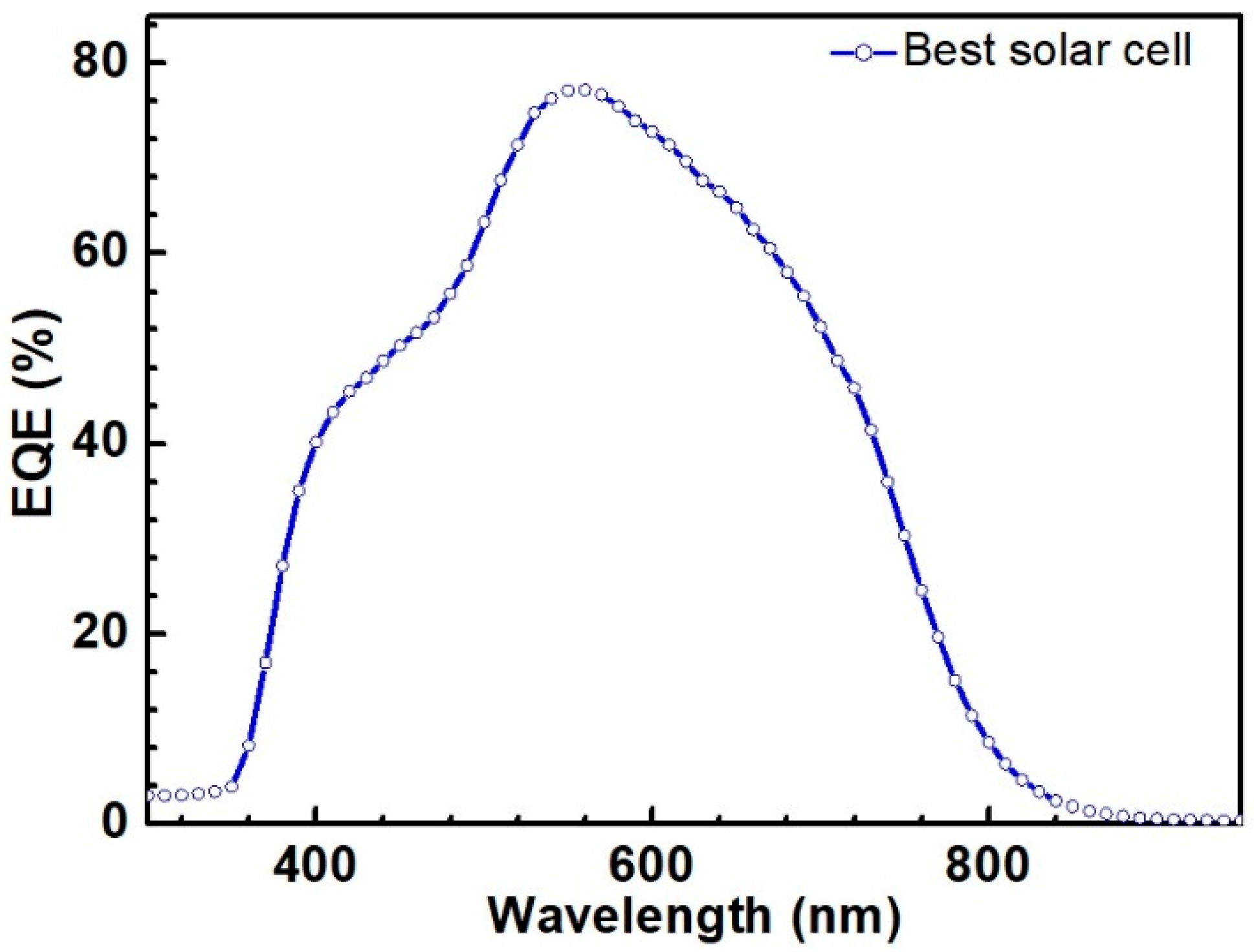
Figure 10. shows the external quantum efficiency (EQE) curve of the best CZTS solar cell with the annealing temperature of 600 °C. The QE curve shows an abrupt drop near the wavelength of 770 nm, which was attributed to CZTS absorption edge. Thus, the bandgap of the CZTS films was calculated to be about 1.61 eV. The features near 510 nm and 380 nm corresponded to the absorption edges of the CdS and ZnO layers [27], respectively, which was common when using the CdS buffer and ZnO window layers. Based on the EQE data of a solar cell, JSC was calculated as [28]:
where q is the elementary charge, QE is quantum efficiency, and bs is solar flux or irradiation. The sunlight spectrum data are available from Reference [29] for air mass 1.5. Based on Equation (1), Figure 10 and the solar irradiation spectrum, JSC of the CZTS solar cell was calculated as 17.5 mA/cm2 for a solar cell annealed at 600 °C. It can be seen that Jsc calculated from the QE curve deviated from the J-V curve. One explanation for the result is that the J-V curve represents the real performance of a photovoltaic device, but the QE measurement was carried out at a single wavelength with much lower intensity than that of a one sun irradiation.
4. Conclusions
CZTS precursor is deposited by nanocrystal ink using a spin-coating method. The precursor is then annealed in the sulfur atmosphere under different temperatures. Raising temperature can promote the growth of grain size of CZTS films and when the temperature is over 625 °C pinholes that stretch through the film begin to appear. Increasing temperature can increase the sulfur vapor pressure as well, leading to the conversion of sulfur-poor films to sulfur-rich films. According to the XRD pattern, the crystallinity of CZTS films is significantly improved by the high temperature, and secondary phase of ZnS begins to show up when the annealing temperature is increased to 625 °C. Judging from the Raman scattering spectra, the secondary phase of ZnS mainly exist in the large particles on the surface of the film, related to the decomposition of CZTS films. With the increase of annealing temperature, solar cell performance increases and the best conversion efficiency of 7.5% is obtained when the annealing temperature is 600 °C.
Author Contributions
Conceptualization: X.Z. Part of the characterization: E.F. Funding acquisition: Y.W. Draft review and editing: M.Z.
Funding
Part of the work was financially supported by a Grant for Special Research Projects of Zhongshan Institute (Funding No. 417YKQ10) and Young Innovative Talents Project for Colleges and Universities in Guangdong Province (2016KQNCX199). This work was also financially supported by the National Science Foundation of China (Grant Nos. 61302044 and 61671140) and Key Project of Science and Technology Plan of Zhongshan City (Grant No. 2018B1018).
Acknowledgments
We thank Edanz Group for editing a draft of this manuscript.
Conflicts of Interest
The authors declare no conflict of interest. The funders contributed in collecting results and editing the manuscript.
References
- Khoshsirat, N.; Bradford, J.; Shahbazi, M.; Zhang, S.L.; Shafiei, M.; Wang, H.X.; Motta, N. Efficiency Enhancement of Cu2ZnSnS4 Thin Film Solar Cells by Chromium Doping. Sol. Energy Mater. Sol. C 2019, 201, 110057. [Google Scholar] [CrossRef]
- Katagiri, H.; Jimbo, K.; Maw, W.S.; Oishi, K.; Yamazaki, M.; Araki, H.; Takeuchi, A. Influencing Mechanism of Cationic Ratios on Efficiency of Cu2ZnSn(S, Se)4 Solar Cells Fabricated with DMF-based Solution Approach. Sol. Energy Mater. Sol. C 2019, 195, 55–62. [Google Scholar]
- Guo, Q.J.; Ford, G.M.; Yang, W.C.; Walker, B.C.; Stach, E.A.; Hillhouse, H.W.; Agrawal, R. Fabrication of 7.2% Efficient CZTSSe Solar Cells Using CZTS Nanocrystals. J. Am. Chem. Soc. 2010, 132, 17384–17386. [Google Scholar] [CrossRef] [PubMed]
- Ahmed, S.; Reuter, K.B.; Gunawan, O.; Guo, L.; Romankiw, L.T.; Deligianni, H. A High Efficiency Electrodeposited Cu2ZnSnS4 Solar Cell. Adv. Energy Mater. 2012, 2, 253–259. [Google Scholar] [CrossRef]
- Abous-Ras, D.; Kirchartz, T.; Rau, U. Advanced Characterization Techniques for Thin Film Solar Cells, 1st ed.; WILEY-VCH Verlag GmbH&Co. KGaA: Weinheim, Germany, 2011; p. 6. [Google Scholar]
- Wang, W.; Winkler, M.T.; Gunawan, O.; Gokmen, T.; Todorov, T.K.; Zhu, Y.; Mitzi, D.B. Device Characteristics of CZTSSe Thin-Film Solar Cells with 12.6% Efficiency. Adv. Energy Mater. 2014, 4, 1301465. [Google Scholar] [CrossRef]
- Woo, K.; Kim, Y.W.; Moon, J. A Non-toxic, Solution-processed, Earth Abundant Absorbing Layer for Thin-Film Solar Cells. Energy Environ. Sci. 2012, 5, 5340–5345. [Google Scholar] [CrossRef]
- Collord, A.D.; Hillhouse, H.W. Composition Control and Formation Pathway of CZTS and CZTGS Nanocrystal Inks for Kesterite Solar Cells. Chem. Mater. 2015, 27, 1855–1862. [Google Scholar] [CrossRef]
- Fella, S.; Carolin, M.; Uhl, A.R.; Romanyuk, Y.E.; Tiwari, A.N. Large-grained Cu2ZnSnS4 Layers Sintered from Sn-rich Solution-deposited Precursors. Phys. Status Solidi A 2015, 212, 121–125. [Google Scholar] [CrossRef]
- Akter, J.F.; Zaman, S.M.; Junaebur, R.M. Towards High-efficiency CZTS Solar Cell through Buffer Layer Optimization. Mater. Renew. Sustain. Energy. 2019, 8, 6. [Google Scholar] [CrossRef]
- Zhang, X.F.; Fu, E.G.; Wang, Y.H.; Zhang, C. Fabrication of Cu2ZnSnS4 (CZTS) Nanoparticle Inks for Growth of CZTS Films for Solar Cells. Nanomaterials 2019, 9, 336. [Google Scholar] [CrossRef]
- Zhang, X.F.; Wu, H.D.; Fu, E.G.; Wang, Y.H. In-Depth Characterization of Secondary Phases in Cu2ZnSnS4 Film and Its Application to Solar Cells. Nanomaterials 2019, 9, 855. [Google Scholar] [CrossRef] [PubMed]
- Scragg, J.J.; Ericson, T.; Kubart, T.; Edoff, M.; Platzer-Bjorkman, C. Chemical Insights into the Instability of Cu2ZnSnS4 Films during Annealing. Chem. Mater. 2011, 23, 4625–4633. [Google Scholar] [CrossRef]
- Jiang, J.C.; Zhang, L.Q.; Wang, W.; Hong, R.J. The Role of Sulphur in the Sulfurization of CZTS Layer Prepared by DC Magnetron Sputtering from a Single Quaternary Ceramic Target. Ceram. Int. 2018, 144, 11597–11602. [Google Scholar] [CrossRef]
- Shin, B.; Gunawan, O.; Zhu, Y.; Bojarczuk, N.A.; Chey, S.J.; Guha, S. Thin Film Solar Cell with 8.4% Power Conversion Efficiency Using an Earth-abundant Cu2ZnSnS4 Absorber. Prog. Photovolt. 2013, 21, 72–76. [Google Scholar] [CrossRef]
- Agasti, A.; Mallick, S.; Bhargava, P. Electrolyte pH Dependent Controlled Growth of Co-electrodeposited CZT Films for Application in CZTS based Thin Film Solar Cells. J. Mater. Sci. Mater. Electron. 2018, 29, 4065–4074. [Google Scholar] [CrossRef]
- Fernandes, P.A.; Salomé, P.M.P.; da Cunha, A.F. Study of Polycrystalline Cu2ZnSnS4 Films by Raman Scattering. J. Alloy. Compd. 2011, 509, 7600–7606. [Google Scholar] [CrossRef]
- Fairbrother, A.; Fourdrinier, L.; Fontané, X.; Izquierdo-Roca, V.; Dimitrievska, M.; Pérez-Rodríguez, A.; Saucedo, E. Precursor Stack Ordering Effects in Cu2ZnSnSe4. Thin Films Prepared by Rapid Thermal Processing. J. Phys. Chem. C 2014, 118, 17291–17298. [Google Scholar] [CrossRef]
- Yoo, H.; Kim, J.H.; Zhang, L.X. Sulfurization Temperature Effects on the Growth of Cu2ZnSnS4 Thin Film. Curr. Appl. Phys. 2012, 12, 1052–1057. [Google Scholar] [CrossRef]
- Khare, A.; Himmetoglu, B.; Johnson, M.; Norris, D.J.; Cococcioni, M.; Aydi, E.S. First Principles Calculation of the Electronic Properties and Lattice Dynamics of Cu2ZnSn(S1−xSex)4. J. Appl. Phys. 2012, 111, 083707. [Google Scholar] [CrossRef]
- Fontané, X.; Izquierdo-Roca, V.; Saucedo, E.; Schorr, S.; Yukhymchuk, V.O.; Valakh, M.Y.; Pérez-Rodríguez, A.; Morante, J.R. Vibrational Properties of Stannite and Kesterite Type Compounds: Raman Scattering Analysis of Cu2(Fe, Zn)SnS4. J. Alloy. Compd. 2012, 539, 190–194. [Google Scholar] [CrossRef]
- Brafman, O.; Mitra, S.S. Raman Effect in Wurtzite- and Zinc-Blende-Type ZnS Single Crystals. Phys. Rev. 1968, 171, 931–934. [Google Scholar] [CrossRef]
- Sharma, T.; Natasha; Kapoor, A. Synthesis and Study of ZnS Nanoparticles for Photovoltaic Application. Adv. Sci. Lett. 2016, 22, 1059–1063. [Google Scholar] [CrossRef]
- Ren, Y.; Richter, M.; Keller, J.; Redinger, A.; Unold, T.; Donzel-Gargand, O.; Scragg, J.J.S.; Platzer Björkman, C. Investigation of the SnS/Cu2ZnSnS4 Interfaces in Kesterite Thin-Film Solar Cells. ACS Energy Lett. 2017, 2, 976–981. [Google Scholar] [CrossRef]
- Ren, Y.; Scragg, J.J.S.; Frisk, C.; Larsen, J.K.; Li, S.Y.; Platzer-Björkman, C. Influence of the Cu2ZnSnS4 Absorber Thickness on Thin Film Solar Cells. Phys. Status Solidi A 2015, 212, 2889–2896. [Google Scholar] [CrossRef]
- Fontane, X.; Calvo-Barrio, L.; Izquierdo-Roca, V.; Saucedo, E.; Perez-Rodriguez, A.; Morante, J.R.; Berg, D.M.; Dale, P.J.; Siebentritt, S. In-depth Resolved Raman Scattering Analysis for the Identification of Secondary Phases: Characterization of Cu2ZnSnS4 Layers for Solar Cell Applications. Appl. Phys. Lett. 2011, 98, 181905. [Google Scholar] [CrossRef]
- Ramanathan, K.; Contreras, M.A.; Perkins, C.L.; Asher, S.; Hasoon, F.S.; Keane, J.; Young, D.; Romero, M.; Metzger, W.; Noufi, R.; et al. Properties of 19.2% Efficiency ZnO/CdS/CuInGaSe2 Thin-Film Solar Cells. Prog. Photovolt. 2003, 11, 225–230. [Google Scholar] [CrossRef]
- Nelson, J. Physics of Solar Cells, 1st ed.; Imperial College Press: London, UK, 2003; p. 7. [Google Scholar]
- Christians, J.A.; Manser, J.S.; Kamat, P.V. Best Practices in Perovskite Solar Cell Efficiency Measurements. Avoiding the Error of Making Bad Cells Look Good. J. Phys. Chem. Lett. 2015, 6, 852–857. [Google Scholar] [CrossRef]
Figure 1.
Surface morphology of CZTS films; (a) precursor; (b) 550 °C; (c) 575 °C; (d) 600 °C; (e) 625 °C; (f) 650 °C.
Figure 1.
Surface morphology of CZTS films; (a) precursor; (b) 550 °C; (c) 575 °C; (d) 600 °C; (e) 625 °C; (f) 650 °C.

Figure 2.
Cross-sectional morphology of CZTS films; (a) precursor (b) 550 °C; (c) 575 °C; (d) 600 °C; (e) 625 °C; (f) 650 °C.
Figure 2.
Cross-sectional morphology of CZTS films; (a) precursor (b) 550 °C; (c) 575 °C; (d) 600 °C; (e) 625 °C; (f) 650 °C.

Figure 3.
XRD pattern of CZTS precursor and annealed films.

Figure 4.
XRD pattern of (112) plane of annealed CZTS films.

Figure 5.
Raman spectra of CZTS films with different annealing temperatures (magnification of object lens: 100×).
Figure 5.
Raman spectra of CZTS films with different annealing temperatures (magnification of object lens: 100×).

Figure 6.
3D microscope image of CZTS film annealed at 625 °C. The marks illustrated the area where Raman measurement were conducted.
Figure 6.
3D microscope image of CZTS film annealed at 625 °C. The marks illustrated the area where Raman measurement were conducted.

Figure 7.
Raman spectra of different areas marked in Figure 5 (magnification of object lens: 0.9×).
Figure 7.
Raman spectra of different areas marked in Figure 5 (magnification of object lens: 0.9×).

Figure 8.
Growth mechanism of CZTS films.

Figure 9.
Dependence of solar cell performance on the annealing temperature.

Figure 10.
Quantum efficiency of the best CZTS solar cells annealed at 600 °C.


Table 1.
Composition of CZTS films annealed with different temperature.
| Temperature (°C) | Cu | Zn | Sn | S | Zn/Sn | Sn/(Zn + Sn) |
|---|---|---|---|---|---|---|
| Precursor | 25.6 | 9.7 | 15.1 | 49.6 | 0.64 | 0.61 |
| 550 | 25.0 | 10.0 | 14.9 | 50.1 | 0.67 | 0.60 |
| 575 | 24.1 | 9.6 | 15.0 | 51.3 | 0.64 | 0.61 |
| 600 | 25.1 | 9.3 | 15.4 | 50.2 | 0.60 | 0.62 |
| 625 | 24.7 | 9.8 | 15.1 | 50.5 | 0.65 | 0.61 |
| 650 | 25.3 | 10.6 | 15.0 | 49.1 | 0.70 | 0.59 |
© 2019 by the authors. Licensee MDPI, Basel, Switzerland. This article is an open access article distributed under the terms and conditions of the Creative Commons Attribution (CC BY) license (http://creativecommons.org/licenses/by/4.0/).
Share and Cite
MDPI and ACS Style
Zhang, X.; Fu, E.; Zheng, M.; Wang, Y. Fabrication of Cu2ZnSnS4 Thin Films from Ball-Milled Nanoparticle inks under Various Annealing Temperatures. Nanomaterials 2019, 9, 1615. https://doi.org/10.3390/nano9111615
AMA Style
Zhang X, Fu E, Zheng M, Wang Y. Fabrication of Cu2ZnSnS4 Thin Films from Ball-Milled Nanoparticle inks under Various Annealing Temperatures. Nanomaterials. 2019; 9(11):1615. https://doi.org/10.3390/nano9111615
Chicago/Turabian StyleZhang, Xianfeng, Engang Fu, Maoxi Zheng, and Yuehui Wang. 2019. "Fabrication of Cu2ZnSnS4 Thin Films from Ball-Milled Nanoparticle inks under Various Annealing Temperatures" Nanomaterials 9, no. 11: 1615. https://doi.org/10.3390/nano9111615
Note that from the first issue of 2016, this journal uses article numbers instead of page numbers. See further details here.