3.1. Cyclic Voltametery
Initially, we have performed cyclic voltammetry (CV) to investigate the mechanism of the electrochemical process involving the reduction of nano-SiO
2 to Si on the graphite -WE in CaCl
2 melt at 855 °C. CV has been performed by a linear potential sweep (
E), applied on the graphite-WE with respect to the Mo reference electrode (Mo-RE) at a scan rate of 10 mV/s. Shown in
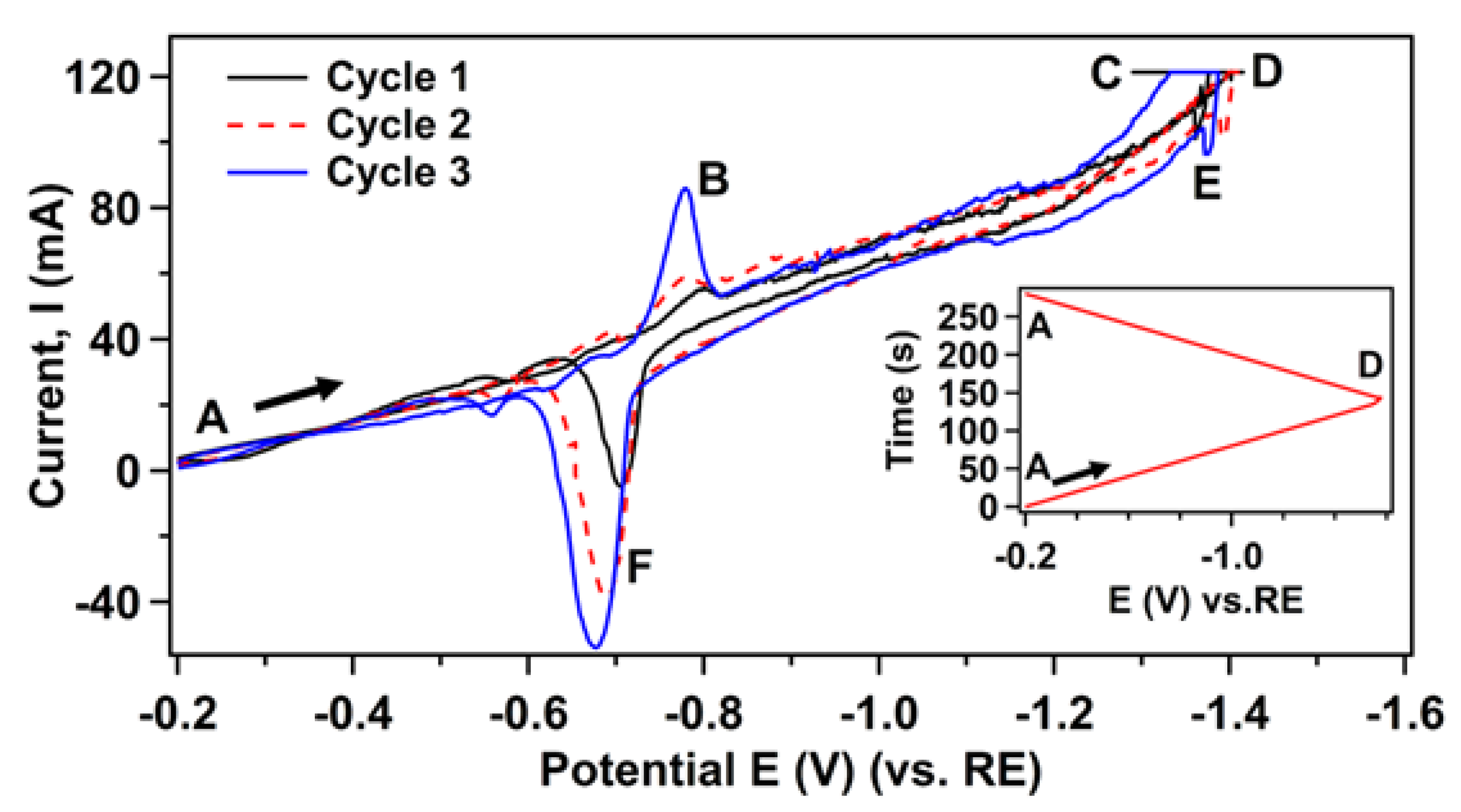
Figure 1 is the CV curve where the x-axis represents the applied potential (
E), while the y-axis is the corresponding resulting current. The arrow in the CV curve indicates the direction in which the potential is scanned. The potential scan was repeated for three-cycles, and the inset of
Figure 1 shows one complete cycle of the potential sweep. In one complete cycle, the potential is firstly scanned from the starting potential of −0.2 V (point A) to the more negative potential of −1.6 V (point D). This is referred to as the cathodic trace. The scan direction is then reversed, and the potential is swept positively back to (−0.2 V, point A), referred to as the anodic trace. As seen from the figure, during the cathodic scan (−0.2 V to −1.6 V) a gradual increase of the current appears starting after −1.0 V vs. graphite RE (cycle-1). We attribute this increase of the current due to the reduction of the nano-SiO
2, where SiO
2 starts to be reduced locally to make Si at the graphite WE.
Further scanning to more negative potential than −1.3 V leads to the faster increase of the reduction current up to the limit of the potentiostat used in this experiment. This high reduction current at this potential has been attributed to the reduction of CaCl
2 to Ca
2+ (cycle-1, point C) and the formation of Si-Ca alloys [
19]. Indeed, according to the phase diagram of the Si–Ca system, several Si-Ca compounds occur at 855 °C [
28]. When the sweeping potential is reached at point D, the scan direction is reversed, and the potential is scanned in the positive (anodic) direction. During the reversed scan, some features are observed around −1.4 to −1.5 V (point E), which could be attributed to the anodic dissolution of Si-Ca compounds. Thus, features at point C and E might be attributed to the formation–deformation of Si–Ca alloy [
16]. As the applied potential becomes more positive, the Si present at the graphite- WE electrode is oxidized back to SiO
2 making a thin layer of SiO
2 on the graphite-WE. An anodic current peak is therefore observed (point F). After continuing to the cathodic scan (−0.2 V to −1.6 V) at cycle-2, a new reduction peak appears around −0.8 V vs. graphite RE (cycle-2, point B), which corresponds to the re-reduction of the formed thin SiO
2 layer deposited during the previous cycle. A similar tendency of the appearing of the reduction and oxidation peaks was observed at the CV on Mo and Ag electrode in SiO
2 containing the CaCl
2 melt [
15,
16,
18]. With a repetition of the scan cycles, both reduction and oxidation peaks shift to corresponding higher potential making larger peak separation. This roughly suggests that electrochemical kinetics becomes more slower with time in the next cycle. In the case of the cathodic scan, this slow electrode kinetics is associated with the requirement of the higher reduction potential, thus making shifting of the peaks to a more negative potential. In addition, as the cycle scan is repeated (cycle-2, cycle-3), the peak height of both reduction and oxidation peaks gradually increases. This suggests a broadening of the reduction-oxidation interface due to the formation of Si-based diffusion layer on graphite [
29]. Once we confirmed the required potential for the reduction of nano SiO
2, we performed an electrochemical reduction at a constant potential (i.e., the chronoamperograms (CA) technique for the formation of electrodeposited Si-layer on the graphite-WE). In a three-electrode based electrochemical system, CA is performed by applying a step potential (in fact, over potential which is more than the required value to initiate the reduction reaction) between WE and RE, and the resulting reduction current, which is proportional to the applied step potential, plays a role in the electrochemical reduction of SiO
2 in molten CaCl
2. To investigate the effect of the reduction potential on the quality and microstructural properties of the deposited Si-layers, we applied different constant reduction potentials for the electrodeposition of Si from nano-SiO
2 on graphite-WE. The constant reduction potentials are conducted in the range of
E = −1.15 to −1.25 V with respect to Mo-RE. Based on the voltammetric results, these potential values are well above the required potential (overpotential) for SiO
2 reduction (i.e., above −1.00 V). However, below enough for the reduction of Ca
2+ (−1.3 V), it was possible to avoid the formation of Si-Ca alloy in the deposited Si-films. In fact, electrochemical reduction with applied reduction potential,
E = −1.00 V resulted in no formation of Si-layer on the graphite as confirmed visually and also with Raman measurement. Thus, in this paper, we define three reduction potentials, namely
low potential (
E = −1.15 V),
moderate potential (
E = −1.20 V), and
high potential (
E = −1.25 V). Material properties of electrodeposited Si-layer were investigated in relation to these defined reduction potentials.
3.2. Structural and Crystal Properties
Shown in
Figure 2a is the XRD plot of the samples prepared by constant reduction potential of
low potential (
E = −1.15 V) and
high potential (
E = −1.25 V) versus Mo-RE. To avoid the strong peaks from graphite substrates in the XRD patterns, we have peeled off the Si-layers from the graphite-WE and ground them to powder to conduct the XRD experiment. XRD of the graphite rod after peeling off the Si-layers was also taken. In addition, to confirm the peak positions of the electrodeposited Si, the XRD pattern of a crystalline Si has also been plotted in the same figure as a reference (ICDD standard: 00-027-1402). As seen from the figure, XRD patterns clearly confirm the formation of silicon (Si) phases on graphite substrates. In addition, it can be seen that with an increase of the reduction potential from
low potential to
high potential, the intensity of the XRD peaks increases and peaks become sharper with a decrease of the full width at half maximum (FWHM). Moreover, Gaussian analysis of the (111) diffraction plane (
Figure 2b) shows a peak shift to 2θ = 28.88° for the sample deposited at
low potential compared to the reference peak position at 2θ = 28.44°. Peak shift decreases to 2θ = 28.56° for the sample deposited at
high potential. Roughly, this peak shift to the higher angle compared to the reference Si-peak can be attributed to the lattice contraction or formation of microstrain in the Si-deposits, the magnitude of which decreases with an increase of the reduction potential. The crystallite sizes of the Si-deposits are correlated with the broadening of the XRD peaks and can be calculated using Scherrer’s equation [
30]:
Here,
D is the mean size of the crystallites or coherently ordered crystalline domain (nm),
K is a constant related to crystallite shape, normally taken as 0.94 for cubic structure,
λ is the X-ray wavelength with the value of 1.54056 Å in the case of CuKα1 radiation,
β is the full width at half the maximum (radians) of the X-ray diffraction peak, and
θ is the Bragg diffraction angle (in degree). Gaussian fitting of the (111) peaks in both samples was used to determine FWHM and peak position. The calculated results of the crystalline size using the fitting parameters were found as 34.14 nm and 15.15 nm for Si samples, electrodeposited at
high potential and
low potential, respectively. It should be noted that Scherrer’s formula provides only the lower limit of the crystallite size, which may be smaller or equal to the grain size or particle size. In addition, the broadening of the XRD peaks might also be correlated to the inhomogeneous lattice strain as we mentioned above, and also to lattice defects. In fact, a rough estimation of the microstrain (ε) based on the (111) diffraction plane, and using the equation [
31],
gives a value of
ε = 4.3 × 10
−3 radian and 9.6 × 10
−3 radian for the Si deposits obtained at
high potential and
low potential, respectively. Hence, it can be assumed that increased negative reduction potential leads to the increase of the particle size along with the increased crystallinity of the electrochemically obtained Si-deposits.
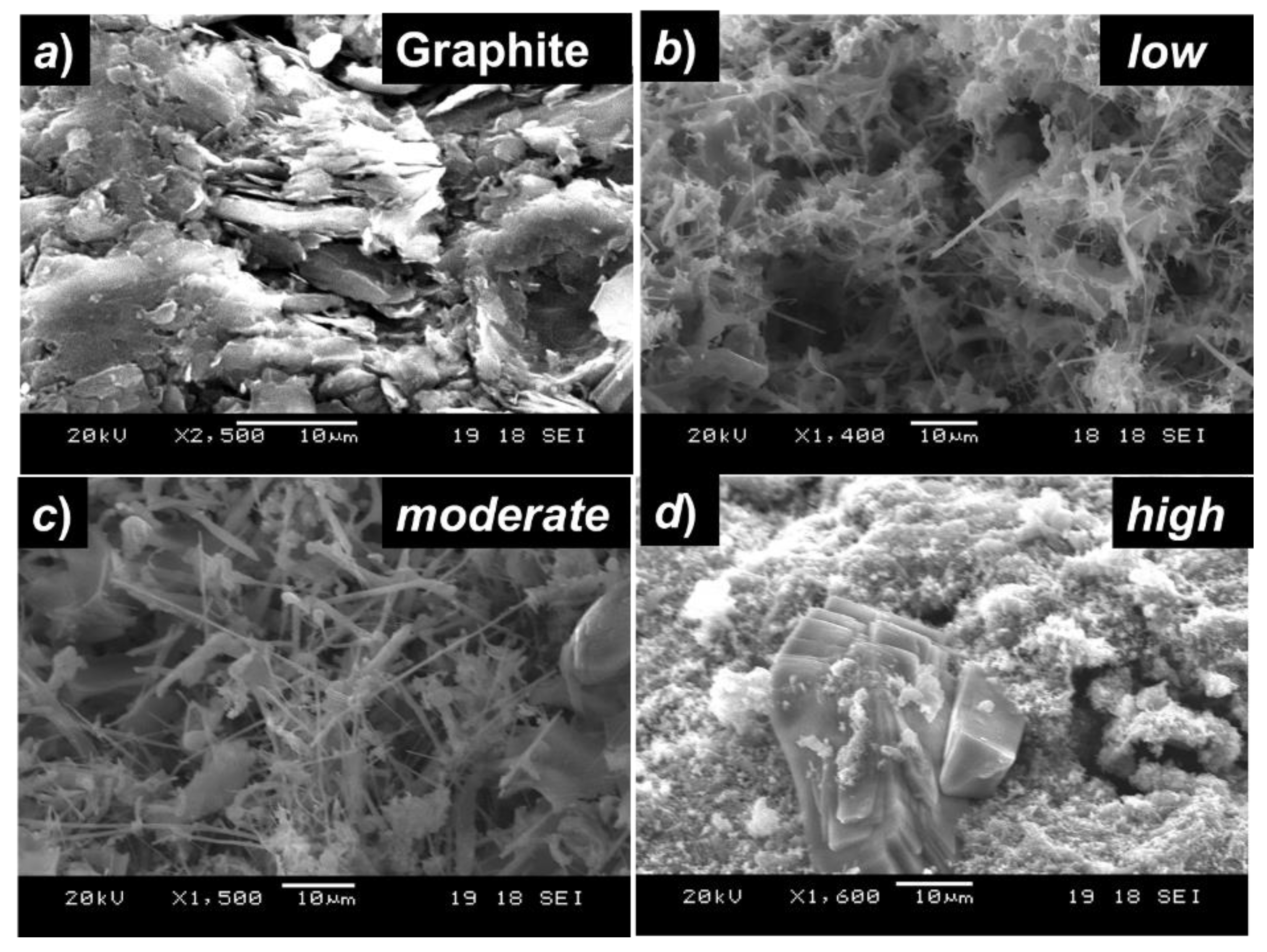
Later, we have investigated the microstructural properties and morphology of the electrodeposited Si-layers on the graphite-substrates using SEM as shown in
Figure 3. As seen from
Figure 3a, before deposition, graphite substrate shows a smooth morphology with a layered structure. Si-layer obtained with applying a
low potential mainly consisted of Si nanowires [
Figure 3b], with a diameter estimated from SEM image is up to hundreds of nm. With an increase of the reduction potential to
moderate potential, the morphology of the deposit transfers to a mixture of Si nanowires of increased diameters and agglomerated Si nanoparticles, as can be seen from
Figure 3c. However, with increased reduction potential to
high potential, Si nanowires disappeared and relatively larger grains of Si, embedded into the matrix of Si-nanoparticles were observed [
Figure 3d]. Thus, the size, shape, and morphology of the electrodeposited Si-layers on graphite substrates seem to be dependent on the applying reduction potential during electrochemical reduction of nano-SiO
2. H. Xie et al. [
20] also reported a similar dependence of the morphology of Si-films on the reduction potentials during electrochemical reduction of nano-SiO
2 on graphite substrates, conducted in a two-electrode-based electrochemical system. The size and morphology of the deposited Si-nanowires on graphite also depend on the cathodic current densities, as has been reported by Peng et al. [
22], where their group performed constant current electrolysis of SiO
2 in molten KCl-KF-1 mol% K
2SiF
6 salt at 650 °C.
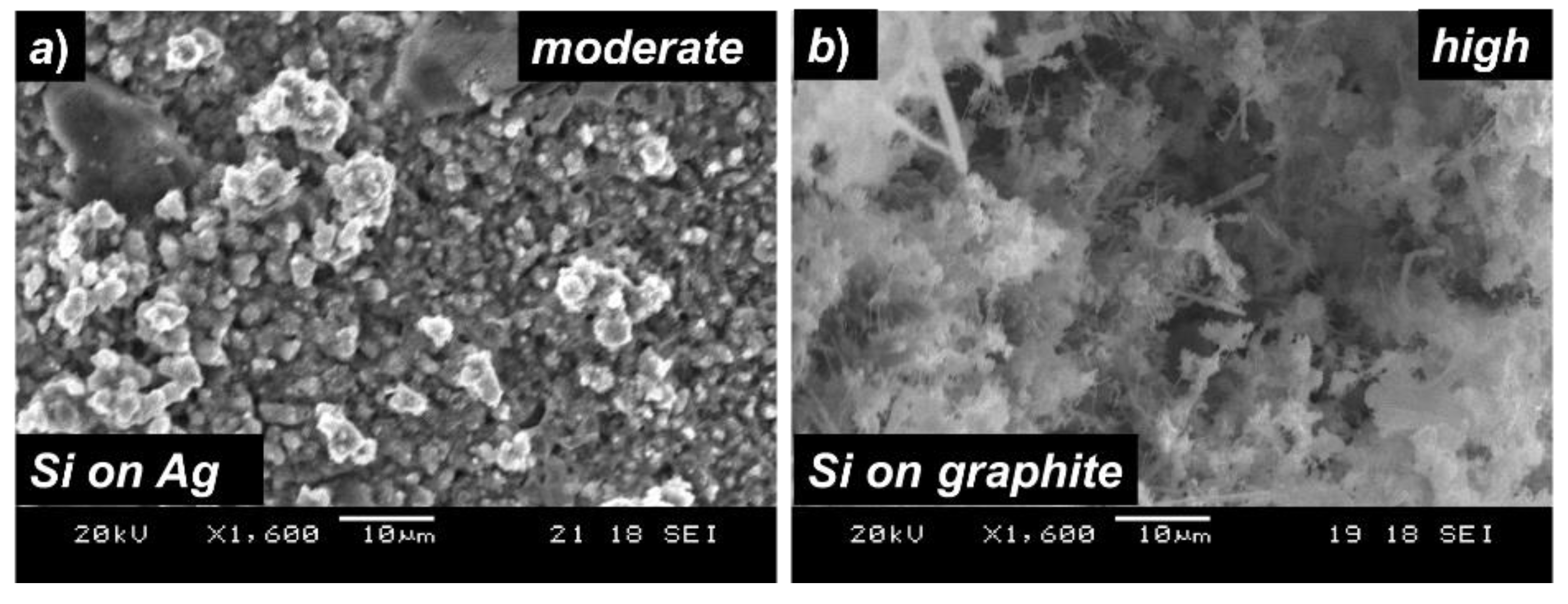
The similar group also reported that during electrolysis, the addition of a small amount of tin (Sn) into the liquid melt assist in the formation of a dense and thick layer of Si on the graphite substrates, where morphology shows larger grains of Si, with no formation of Si nanowires. The author attributed the lateral growth (granular) of the Si particles to the mediator role of Sn, which is associated with enhanced surface diffusion properties at the growth temperature of 650 °C, mainly due to its metallic bonding compared to the only covalently bonded Si in the absence of Sn. In fact, in our previous study [
16], we have investigated the effect of reduction potential on the electrochemical formation of Si-layer on Ag substrates from nano-SiO
2. Although the crystalline size was observed to be increased from nanoscale to the microscale level with an increase of the applied potentials, no nanowire formation has been observed even at the lower reduction potential of
E = −1.00 V (with respect to graphite-RE). In this study, to confirm the effect of substrate materials on the morphology, we have deposited Si-layer on an Ag-foil with a reduction potential equivalent to
moderate potential (
E = −1.20 V with respect to graphite-RE) from similar nano-SiO
2 as feed materials, while keeping the other growth parameters similar to the conditions used in case of graphite substrates. Shown in
Figure 4a is the SEM image of the electrodeposited Si-layer on the Ag-substrate. As seen from the figure, the morphology of the deposited Si-film shows the granular shapes with no formation of nanowires. In fact, electrochemical formation of the Si-layer on other metal-substrates (e.g., Mo, Ni) has been reported to show granular growth of deposited layers [
18,
32]. Thus, it can be considered that substrate-metals at a higher growth temperature decide the formation and growth orientation of the nuclei at the initial stage and play a role in determining the final shape and morphology of the grown films. The rate of nuclei formation, orientation, and size of the final grains should also then be related to the electron transfer rate from metal to SiO
2, which in turn might be related to the mobility and diffusion properties of metal into SiO
2 at a higher growth temperature. The formation of any liquid droplets or mixed phase of metal-Si at the growth temperature may also affect the morphology and grain size of the deposited films.
However, it is interesting to note that electrochemical reduction of solid silica (in any forms, e.g., quartz substrates, SiO
2 pellet, etc.) with in-contact with metals including Mo, Ni, W etc. in high-temperature molten salt has been reported to form nanowires, especially at the region of solid-silica/metal-contact interface [
11,
19,
33,
34]. Thus, it can be assumed that the size of the crystalline domain of the feed materials may also play roles in defining the morphology of the Si-layers during the electrochemical reduction process. Thus, to understand the size-effect of the SiO
2 particles on the morphology of the electrochemically obtained Si-layer on the same graphite substrate, we have deposited a Si-layer on the graphite-substrate using SiO
2 feed material with the size of the particles in the range of 300–600 µm. A reduction potential of
E = −1.25 V that is equivalent to
high potential has been applied on graphite-WE with respect to Mo-RE, keeping other growth conditions similar to previous experiments with nano-SiO
2. Shown in
Figure 4b is the SEM surface image of the obtained Si-layer on graphite-substrate, electrochemically reduced from SiO
2 of larger-sized particles. In comparing to the Si-layer obtained from nano-SiO
2, the Si-layer deposited with larger SiO
2 particles shows smaller grain size in nanoscale levels, obtained by applying a similar reduction potential. It has been reported that due to the insulator nature of SiO
2, the electrochemical reduction process of SiO
2 to Si at the graphite/SiO
2 interface is kinetically slow even at a higher reduction temperature of 855 °C [
11]. In fact, the gradual increase of the cathodic current in the CV diagram at
Figure 1 also supports that the reaction kinetics are relatively slow at graphite-WE in the high-temperature melt of SiO
2 and CaCl
2. Thus, the faster dissolution rate of nano-SiO
2 in contact with the graphite-WE at higher growth temperature is associated with faster reduction of SiO
2 and formation of relatively larger grains at the given growth time. On the other hand, a relatively slower dissolution rate of SiO
2 with the larger-sized particles is responsible for a slower reduction rate due to reduced capacity of receiving electrons from substrates, thus making the grains of the Si-films smaller in size. The above observation also explains the formation of small-sized Si-nanowires in solid silica in contact with metal, which could be attributed to the slow reduction rate of solid silica at a given potential. In addition, X. Yang et al. [
23] studied the deposition of Si layers on the graphite substrates from nano-SiO
2 in the mixture of CaCl
2 (4.8 mol%)-CaO (3.9 mol%) molten salt at high temperature. The author reported the formation of dense and crystalline Si, mainly due to the high dissolution rate of nano-SiO
2 originated from the formation of soluble Si
iv-O complex anion with nano-SiO
2 and O
2− in CaO. Morphology of the obtained Si was mainly granular in size without formation of nanowires. Thus, it can be assumed that an increased dissolution rate of nano SiO
2 in the presence of CaO is mainly responsible for faster reduction rate and, thus, the formation of granular morphology, while nano-SiO
2 in molten salt without the addition of CaO is associated with relatively slow reduction rate, and thus should yield the formation of nanowires.
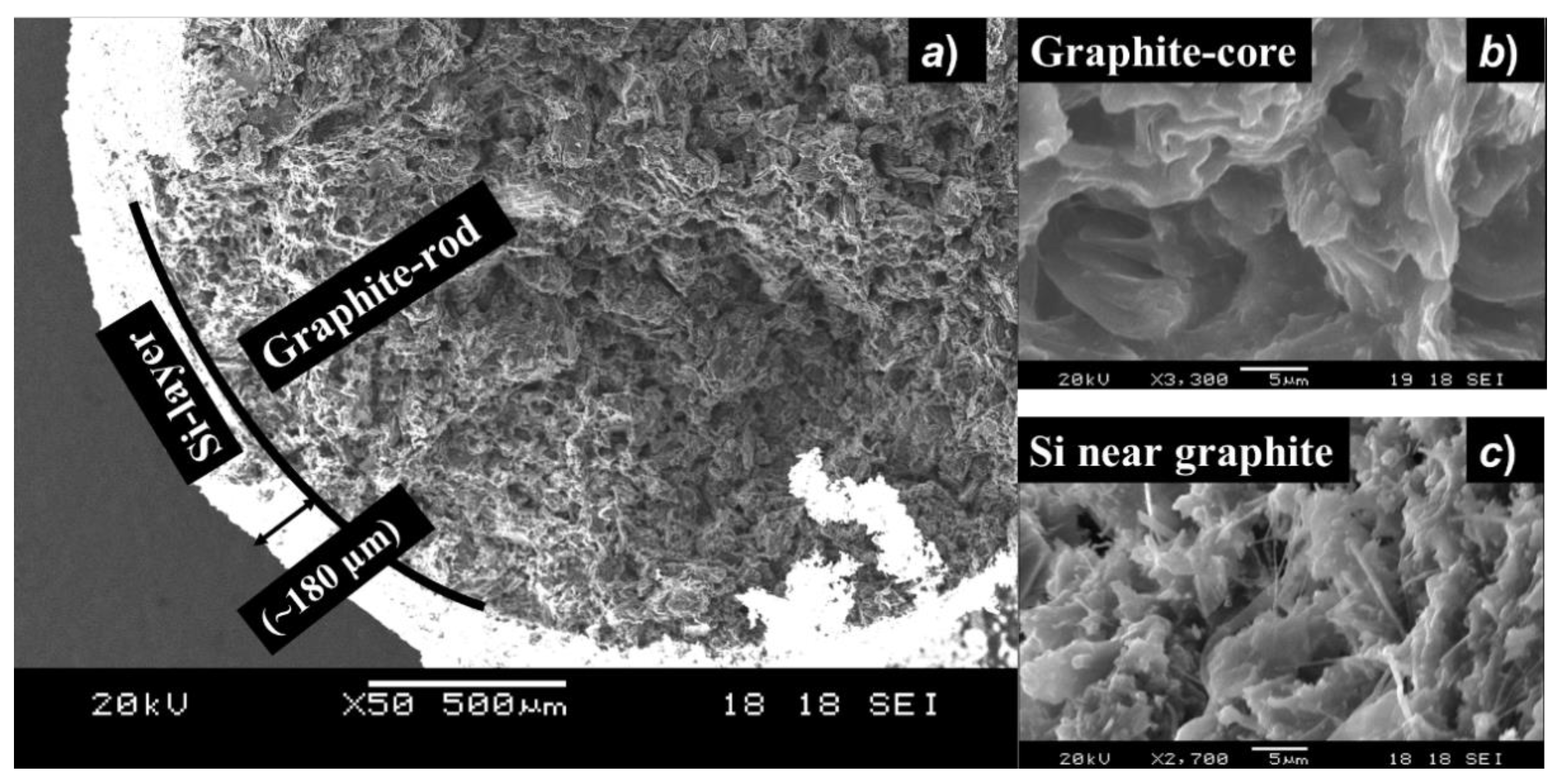
Finally, to understand the growth rate and thickness of the electrodeposited Si-layer, we have performed a cross-sectional SEM of the Si-coated graphite substrate.
Figure 5 shows cross-sectional SEM images of the similar sample (grown with
low potential), the surface of which has been shown in
Figure 3b.
As seen from
Figure 5a, the core consists of the graphite-rod (WE), showing part of a well-defined circle (diameter 3 mm) with a darker color. The core is covered with the deposited Si layer showing brighter color with 100–200 μm of thickness. In the case of graphite substrate, H. Xie et al. [
20] reported a formation of a transition layer at the Si/graphite interface which is consisted of a mixture of elemental Si and C and also SiC phase. The formed SiC could help to the adhesion of deposited Si-layer on the substrate and help to grow thick films. However, it should be noted that the thickness of the Si-films around the graphite rod is not uniform [
Figure S1]. A constant flow of Ar gas (150 mL/min) during the electrochemical reduction process might produce strong convection in the melt of SiO
2 and CaCl
2, mainly due to the temperature gradient at the melt surface and the bottom part of the electrochemical cell. This nonuniform convection affects the diffusion rate of SiO
2 from different locations of the electrochemical cell towards the graphite-WE, and thus affects the reduction rate. Furthermore, the relative position of the graphite-WE and Mo-RE in the electrochemical cell may affect the reduction rate at different locations of the graphite rod, thus making films with non-uniform thickness. Nevertheless, although the thickness of the Si-layer is very large, the morphology of the obtained Si-layer around the graphite-rod (WE) may not be dense and shows a dendrite-type structure. In addition,
Figure 5b shows a magnified SEM image of the core of the graphite-rod (WE), while
Figure 5c shows a magnified SEM image of the Si-coating, roughly close to the graphite substrate. It is interesting to note that although the surface of the sample is composed of mainly Si nanowires with very small dimensions [
Figure 3b], Si particles close to the graphite-rod seem relatively larger in size with very few portions of nanowire phases. It should be noted that the purity of the electrodeposited Si-films in this study has not been confirmed. However, as the kinetic reaction of Si and C is typically slower at a growth temperature of 855 °C, except for the interface at Si/graphite, the surface of the deposited Si-layer is assumed not to contain any mixed phase of Si and C as well as any elemental C diffused from the substrate. Nevertheless, the surface of the Si-deposits may contain a very thin amorphous type SiO
2 phase, originated from the ambient air after HCl washing or through the reaction of evolved O
2− and newly-formed Si nuclei during the electrochemical reduction of SiO
2. Unreacted SiO
2 (if any) during the electrochemical reduction process can also be adsorbed inside the grain boundaries of Si-deposits. In addition, electrochemical reduction of SiO
2 was carried out by applying the negative potential in the range of
E = −1.15 and −1.25 V in the CaCl
2 melt at a temperature of 855 °C. This potential is below the required reduction potential of CaCl
2 (i.e.,
E = −1.30 V) as we can see in the CV diagram in
Figure 1. Thus, the formation of Ca-Si alloy is unlikely in the Si-deposits obtained in this study. Still, obtained Si-deposits may contain contamination of Fe, Al, C, etc. originating from other possible sources such as steel flanges in the electrochemical cell, graphite counter electrode, Al
2O
3 crucible, etc.
Nevertheless, based on the above discussion, we can explain the reduction process as follows. When the applied potential at the graphite-WE (vs. Mo-RE) is more negative than the required reduction potential of SiO
2, then nano-SiO
2, adjacent to the graphite-WE in high-temperature melt receives electrons from conductive graphite, and become reduced to make Si-layer on graphite according to the following equation.
The formed thin layer of Si then plays the role of conducting medium at high temperature, where oncoming melt of nano-SiO2 gets necessary electrons to be reduced on newly formed Si-layer. The growth mechanism, along with the morphological evolution, can be explained in relation to the growth parameters as follows:
- (a)
Substrate: Initially, substrate materials (along with the size of the source materials) determine the growth orientation of Si nuclei, formed just after the reduction on the substrate. At a particular applied reduction potential, faster diffusion properties of high mobility metal substrates (e.g., Ag, Mo, etc.) or added metal particles in the solution enhance faster rate of electron transfer at the substrate/SiO2 interface, thus making larger sized nuclei on the substrate and promoting the lateral growth of the particles.
- (b)
Reduction potential: In the case of graphite- substrate, at lower reduction potentials (low potential), due to the lower rate of electron transfer between graphite and the SiO2 melt, the formation rate of nuclei is slow, making random nucleation sites of few numbers at nanoscale levels, and randomly oriented on the substrates. Further reduction of adjacent nano-SiO2 at the same lower potential promotes anisotropic and directional growth of Si nanowires or nanoparticles. On the other hand, at high potential, due to increased rate of electron transfer, the formation of a larger number of nuclei with increased size allows lateral growth of Si particles by agglomerating Si-islands. With the further proceeding of the reduction process, those Si-particles form larger Si-grains making a Si-layer along the growth front.
- (c)
Particle size of the SiO2: Finally, considering the higher dissolution rate, nano-SiO2 are more favorable to form Si-layers with larger grains in micro or polycrystalline levels at a given reduction potential due to a faster rate of electron transfer. SiO2 granules with larger particle sizes are suitable for the formation of Si at the nanoscale level (nanocrystals or nanowires) at the same reduction potential.
Finally, a schematic diagram of the growth mechanism of Si-films on graphite-substrates has been shown in
Figure 6, where we have considered only favorable conditions for the growth of nanowires and nano/microparticles.
As apparent from the schematic diagram, for a given substrate material, both the dissolution rate of SiO2 in high-temperature molten salt, and/or the transfer rate of electrons at the SiO2/substrate interface are crucial to determine the initial size and growth rate of nuclei formation, which later determine the morphology and microstructural properties of the final Si-deposits. Lower reduction potential and/or large-sized SiO2 feed materials are favorable for the formation of nanowires due to slower growth nuclei, while application of higher reduction potential and/or use of nano-SiO2 are favorable for the formation of laterally grown Si-nano/microparticles. In addition, application of sufficiently low potential alone, even with nano-SiO2 meets the condition for the formation of directionally grown Si-nanowires, while application of adequate high potential with large-size SiO2 particles can form nano/microparticles.
3.3. Optical Properties
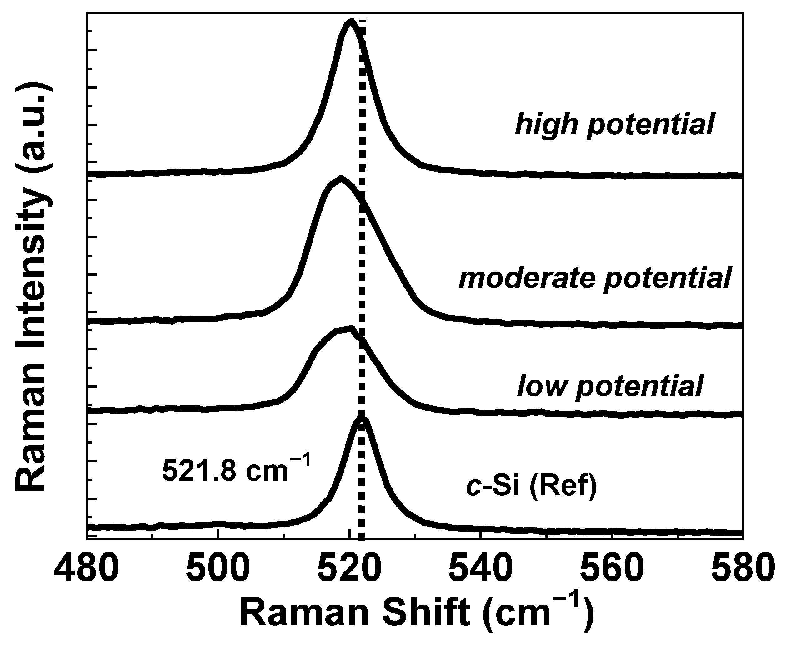
To study the optical properties of the Si-layers on graphite substrates, we have performed µ-Raman spectroscopy of the Si-layers deposited with different reduction potentials as shown in
Figure 7. Raman spectrum of a single crystalline silicon (
c-Si) wafer was also shown in the same figure as a reference. In fact, Raman is a non-destructive method to identify elemental composition including phase or molecules, and also their crystallinity in the sample. As seen from the figure,
c-Si shows a sharp and symmetric peak around 521 cm
−1 [
35], which is associated with the Raman scattering by the Si optical phonon mode. In the case of Si in the amorphous phase, the phonon peak becomes broadened and shifts to lower wavenumbers at around 480 cm
−1 [
36,
37]. As seen from the figure, no such formation of the amorphous phase has been apparent in the Raman spectra of the electrodeposited films, which suggests that Si-layers obtained in this study are basically crystalline in nature (plausibly due to growth at a higher temperature of 855 °C). However, it can be seen from the figure that the Raman peak of the deposited Si-layers slightly shifted to a lower wavenumber (i.e., down shift) comparing to the
c-Si reference peak. Shifting of the optical phonon-band to a lower wavenumber comparing to that of single-crystal Si (bulk) primarily suggests the size-related quantum confinement effect due to the formation of microcrystalline or nanocrystalline phases. In nanostructured materials, the Raman scattering selection rule is relaxed (k = 0) due to increased disorder, originating from the smaller dimension of the crystallites. It causes the first order transition of phonons to shift away from the Brillouin-zone center, causing softening and asymmetric broadening of the phonon modes with a down shift in the Raman spectra [
38,
39]. Broadening of the Raman peaks in the deposited Si-layers may also originate due to the size distribution of the small crystallites in the sample. It is apparent from the figure that the down-shifting of the peak becomes more prominent in the samples deposited with more lower reduction potentials.
This downshift is consistent with our observation in SEM images that samples deposited with low potential mainly promote the formation of Si nanowire and nanoparticles, and the diameter of the nanowire along with grain size becomes larger with an increase of the reduction potential. In addition, as seen from the figure, in general, with an increase in the applied negative potential (i.e., reduction potential), the intensity of the phonon band becomes stronger and FWHM becomes narrower. It also suggests that the crystalline quality of the samples becomes better when electrodeposition is performed with a higher negative potential vs. RE. This observation is also consistent with the XRD and SEM results as discussed before.
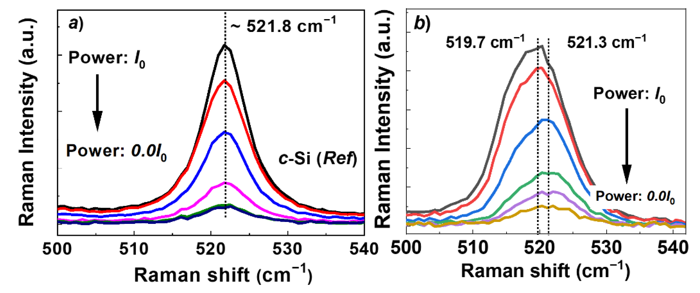
Later, in order to confirm the size-related pure quantum confinement effect in our Si-deposits, we have performed excitation power-dependent Raman spectra. Shown in
Figure 8 are the laser power-dependent Raman spectra of the
c-Si and the Si-deposit obtained at
low potential. As can be seen from
Figure 8a, no noticeable change in the peak position of the optical phonon mode has been observed for the bulk
c-Si sample. However, with an increase of the laser power, the Raman peak of the optical phonon mode shifts to the lower wavenumber (i.e., down shift) for the electrodeposited Si-layer (
Figure 8b). The effect of laser heating on the shift of the Raman-peak in Si nanocrystals has been discussed in the literature [
40,
41]. A down shift of the Raman peak due to laser heating can be attributed to the expansion of the lattice of Si nanocrystals originated from the poor thermal conductivity compared to that of the bulk crystal [
42]. Thus, a down shift of the Raman peak due to the pure quantum confinement effect can be obtained after subtracting the contribution from laser heating effects. Thus, from
Figure 8b, for the Si-deposit obtained at
low potential total down shift comparing to the
c-Si can be estimated around ∆ω = 521.8 cm
−1 − 519.7 cm
−1 = 2.1 cm
−1. Then, neglecting the peak shift due to the heating effect, a down shift due to the quantum confinement effect can be estimated from measurement of the Raman at lowest possible power, which yields a value of around ∆ω = 521.8 cm
−1 − 521.3 cm
−1 = 0.5 cm
−1. It should be noted that tensile strain in the crystal also produces a shifting of the Raman peaks to a lower wavenumber [
43]. Surface oxidation on the Si-layer may also contribute to the shift of the Raman peak. Nevertheless, a systematic downshift of the Raman peak with increasing laser power in the electrodeposited Si-layer confirms the formation of the nanostructured silicon in our study. Later, we have applied the following equation [
44] to roughly estimate the average crystallite size of the Si-deposit obtained at a
low potential, estimated from the downshift of the Raman peak due to size-related quantum confinement effect.
The term
B = 2.24 nm
2 cm
−1 [
45], and Δ
ω = 521.8 cm
−1 − 521.3 cm
−1 = 0.5 cm
−1 as obtained before represents the down shift of the Raman optical phonon mode compared to
c-Si. The average crystallite size of the Si-layer using the above equation has been estimated as 13.33 nm, which is roughly similar to the calculated value of 15.15 nm obtained using Scherrer’s equation [Equation (1)] for the same sample.
Finally, to investigate the luminescent properties of the deposited Si-layers on graphite substrates, we have performed µ-PL of the Si samples. Shown in
Figure 9 are the PL spectra of the Si layers deposited with
low and
high potential. A PL of a single crystal silicon wafer has also been taken and plotted on the same figure. As seen from the figure, PL spectra show asymmetrically broadened features with peaks lying within the wavelength range between 650 and 950 nm, which is lower than the usual crystalline Si-peak around 1150 nm. Primarily this peak shifting suggests the widening of the bandgap of the electrodeposited Si films compared to the single crystal reference films. The widening of the bandgap can be attributed to the presence of nanowires and/or nano/microcrystalline phases in the deposited Si-films [
46]. In nanocrystals, the dimensions of the semiconductors reduce from the bulk to the nanometer level and the band edges start to split into discrete states which gradually increase the optical bandgap, leading to a blue shift of PL peak position (left shift in the wavelength scale) comparing to the bulk crystal [
47]. Thus, shifting of the PL peak to a higher wavelength with an increase in the reduction potentials suggests that the size of the Si crystals becomes larger, and that the crystallinity is enhanced at a higher reduction potential (as can also be seen from Raman and XRD data). It should be mentioned that PL spectra of the electrochemically obtained Si-layer could be affected by a thin, amorphous type SiO
2 layer on the surface as discussed before. It is also worth mentioning that due to nonuniformity, the presence of mixed phases of nanowires, nanoparticles, and crystalline Si, as well as due to dendrite nature of the formed Si-layers, the peak position and intensity of micro-PL and micro-Raman may vary at different locations of a particular sample. Nevertheless, optical characterization of the Si-layers using Raman and PL along with the study of the crystal and the microstructural properties suggests that crystalline-phases, shape, size, and morphology of the electrochemically obtained Si-films on graphite substrates can be controlled by applying the appropriate reduction potential during the electrochemical reduction technique.


 ,
, 


