Tunable Microwave Filters Using HfO2-Based Ferroelectrics


National Institute for Research and Development in Microtechnologies (IMT Bucharest), Erou Iancu Nicolae Street 126A, 077190 Voluntari, Ilfov, Romania
*
Author to whom correspondence should be addressed.
Nanomaterials 2020, 10(10), 2057; https://doi.org/10.3390/nano10102057
Submission received: 9 September 2020
/
Revised: 2 October 2020
/
Accepted: 14 October 2020
/
Published: 18 October 2020
(This article belongs to the Special Issue 2D Materials for Nanoelectronics)
Abstract
:In this paper, we present microwave filters that are based on 6-nm-thick ferroelectric thin films of hafnium oxide doped with zirconium (HfZrO), which are tunable continuously in targeted bands of interest within the frequency range 0.1–16 GHz, when the applied direct current (DC) voltage is swept between 0 V and 4 V. Here, we exploit the orthorhombic polar phase in HfO2 through a careful doping using zirconium in an Atomic Layer Deposition (ALD) process, in order to guarantee phase stabilization at room temperature. Polarization versus voltage characterization has been carried out, showing a remanent polarization (Pr) of ~0.8 μC/cm2 and the coercive voltage at ~2.6 V. The average roughness has been found to be 0.2 nm for HfZrO films with a thickness of 6 nm. The uniform topography, without holes, and the low surface roughness demonstrate that the composition and the structure of the film are relatively constant in volume. Three filter configurations (low-pass, high-pass, and band-pass) have been designed, modelled, fabricated, and fully characterized in microwaves, showing a frequency shift of the minimum of the reflection coefficient between 90 MHz and 4.4 GHz, with a minimum insertion loss of approximately 6.9 dB in high-pass configuration.
1. Introduction
Hafnium oxides (HfO2) have been gathering momentum in the very last years, thanks to their versatility in being exploited for low-power electronics. One of the most appealing characteristics of HfO2 is represented by its electrical permittivity, which can be increased while using structural phase transformations [1]. HfO2 in its most stable phase, i.e., the monoclinic phase, has the lowest permittivity (εr ≈ 18). HfO2 exhibits a much higher permittivity in other phases, such as cubic (εr ≈ 27) or tetragonal (εr ≈ 70), but these phases are stable at temperatures higher than 1700 °C. The increasing of the permittivity of HfO2 is of outmost importance in decreasing the effective oxide thickness (EOT) and, thus, the leakage current, in CMOS transistors when billions of them are integrated in a single silicon (Si) chip. The solution to decrease the temperature in order to obtain a phase transition is the doping of very thin films of HfO2. The cubic phase was attained by doping the HfO2 with yttrium (Y) [1], while the tetragonal phase was obtained by doping with Si [2]. However, the doping with ZrO2 of HfO2 that was grown by atomic layer deposition (ALD) [3,4] has demonstrated the possibility of achieving the tetragonal phase of HfO2 at room temperature. The realization of a high permittivity depends on the concentration of dopants, the annealing temperature, and the growth method; this way, the value of the permittivity of the doped HfO2 could be increased by two–three times from εr ≈ 18 in the monoclinic phase.
The experience gained during years of studies in the enhancement of HfO2 permittivity is the basis of the discovery of the orthorhombic phase that confers ferroelectric properties to HfO2. The same dopants were used as above, but in different growth conditions, since the orthorhombic phase requires very strict control of dopant concentration, temperature, and mechanical strain [5,6]. Cubic and tetragonal, as well as orthorhombic polymorphs of HfO2, can be stabilized by using different dopants, annealing procedures and layer thicknesses. This was demonstrated by ab-initio studies [7] and many experiments reported in the review paper [8].
Nowadays, the most used HfO2-based ferroelectric is the one doped with zirconium (Zr), termed as HfZrO. Can we further enhance the electrical permittivity of HfO2-based ferroelectrics? The answer is positive, since, in any ferroelectric, there is a strong dependency of electrical permittivity on the applied voltage, this property being used extensively in the case of high-frequency devices for tuning their main characteristics [9]. We have recently shown that, in a very large band (1–8 GHz), there is an increase of 27% of the permittivity of HfZrO when a DC bias voltage is swept in the range 0–5 V [10]. Based on these results, the aim of this paper is to show that we can tune the reflection (|S11| or |S22|) and transmission (|S21| or |S12|) coefficients of a low-pass filter (LPF), a high-pass filter (HPF), and a band-pass filter (BPF) when the applied DC voltage is tuned in the range 0–4 V. These circuits are of outmost importance in many areas of wireless communications where filters are ubiquitous components [11]. In detail, there are some key characteristics of HfZrO thin films that make them a target material for (potential) high-performance tunable filters. First, the proposed ferroelectric requires low values of DC bias voltage in order to modulate its dielectric constant. The nanoscale thickness (in the order of some nm) ensures a very large critical (coercive) electric field Ec. A direct consequence of the latter property is the following: large values of Ec entail that small values of an external DC bias voltage (i.e., in the range ±5 V) are enough to tune ferroelectric’s permittivity. This represents a noteworthy advancement with respect to ‘classic’ ferroelectrics, like perovskites (PZTs), as tunable microwave circuits that are based on them need bias values in the order of tens of volts. Second, a full CMOS compatibility is guaranteed, which allows large-scale fabrication. Third, high values of the dielectric constant represent an advantage in designing high-frequency devices with compact dimensions, thanks to a reduction of the guided wavelength. Besides this, the exploitation of ALD techniques gives a further improvement in the overall fabrication process, since it provides precise control of ferroelectric’s thickness, a high homogeneity in terms of surface roughness, and the possibility of using large-area substrates, an undoubtable benefit when testing components for extensive measurements.
2. Materials and Methods
The key of the proposed tunable microwave filters is represented by the voltage- and frequency-dependent dielectric constant of the HfZrO thin film. However, the extraction of the permittivity of HfZrO in microwaves, as a function of the applied DC voltage bias, is a non-trivial problem. ‘Traditional’ methods that are used to analyse multilayer interdigital capacitors (IDCs) or coplanar waveguide (CPW) lines (like single layer reduction or microstrip dual resonator) inevitably fail, since the nanometric scale thickness of the HfZrO ferroelectric thin film makes it impossible to apply analytical methods. Hence, starting from the results that were published in [10,12], via a fitting procedure exploiting electromagnetic (EM) simulations and experiments we can derive the following equation, which expresses the dependence of the relative permittivity ε(V) of the 6-nm-thick HfZrO on the applied voltage, at an assigned frequency:
where 0 < α < 1 V−1 (which depends on the given frequency) is a characteristic constant of HfZrO, whereas εeff(0) is the effective permittivity at 0 V of the HfZrO/bulk substrate, and εeff,bulk is the effective permittivity of the sole bulk substrate. In terms of electric fields:
where t is the thickness of the HfZrO thin film, Ea is the external applied DC electric field, and Ec is the coercive field (i.e., 1–2 MV/cm for HfZrO). Equation (2) is derived in a straightforward way from Equation (1), while taking into account that the DC voltage that is applied to the HfZrO thin film is physically determined by both the external contribution of Ea (which can be estimated also by static EM simulations [10,12]) and the intrinsic contribution of Ec, in order to describe the hysteretic behaviour of the permittivity. These simple relations fit well with the experimental results, if one knows εeff(0) and εeff,bulk (at the desired frequency) that can be easily obtained by either theoretical/simulation results or measurements of scattering parameters. To our knowledge, this approach is the only one feasible for characterizing the high-frequency permittivity of ferroelectric thin films, as other methods take into account either thicker ferroelectrics in vertical capacitor-like configurations or very low frequencies [13,14].
ε(V) = [αV + εeff(0)/(εeff,bulk)1⁄2]2 + εeff(0),
ε(V) = [α(Ea − Ec)t + εeff(0)/(εeff,bulk)1⁄2]2 + εeff(0),
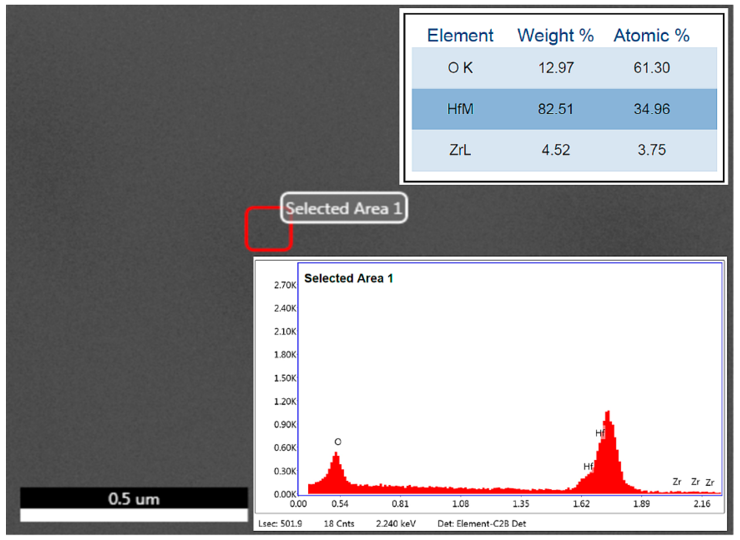
The substrate used for the three filters is a 6-nm-thick Zr-doped HfO2 thin film grown by ALD technique on a 4-inch wafer of 525-μm-thick high-resistivity (HR) Si. An Oxford Instruments OpAL ALD reactor was used for the growing of ferroelectric thin films while using Tetrakis(dimethylamino)hafnium (TDMAH, 99.99+%-Hf, <0.2%-Zr, Strem Chemicals. Inc., Newburyport, MA, USA) and Tetrakis(dimethylamino)zirconium (TDMAZ, 99.99+%-Zr, Strem Chemicals. Inc., Newburyport, MA, USA) as metal organic precursors. Ultra-pure water was used as the oxidant, and ultra-high purity nitrogen (Nitrogen 6.0, 99.9999 vol.%) was used as the purge and carrier gas. Prior to the ALD process, the silicon wafer was subjected to surface cleaning treatment by exposure to UV-ozone for 15 min. at 75 °C, while using an UV-Ozone cleaner (Novascan Technologies Inc., Ames, IA, USA). The ferroelectric HfO2 films were grown by sequentially mixing the two precursors on the silicon wafer surface, in a ratio of 2:1, followed by their oxidation to produce a homogeneous binary oxide. The binary oxide films grown were indexed: HfZrO. The deposition was done with 56 ALD cycles at 200 °C. The film thickness, as measured by X-ray reflectivity (XRR), was found to be around 6 nm. The Ti (10 nm)/Au (360 nm) top metallic circuits (LPF/HPF/BPF) were deposited while using an Electron Beam Evaporation System (Temescal FC2000, Ferrotec, Bedford, NH, USA), and they were photolithographically configured using a standard lift-off process. Due to the low thickness of the HfZrO film, the Energy Dispersive X-ray spectroscopy (EDX) technique can be considered for identifying and quantifying elemental compositions. Figure 1 shows the EDX analysis spectrum of the 6-nm-thick HfZrO film. From the EDX measurements, the film composition was estimated to be HfZrO as Hf0.73Zr0.27O1.85.
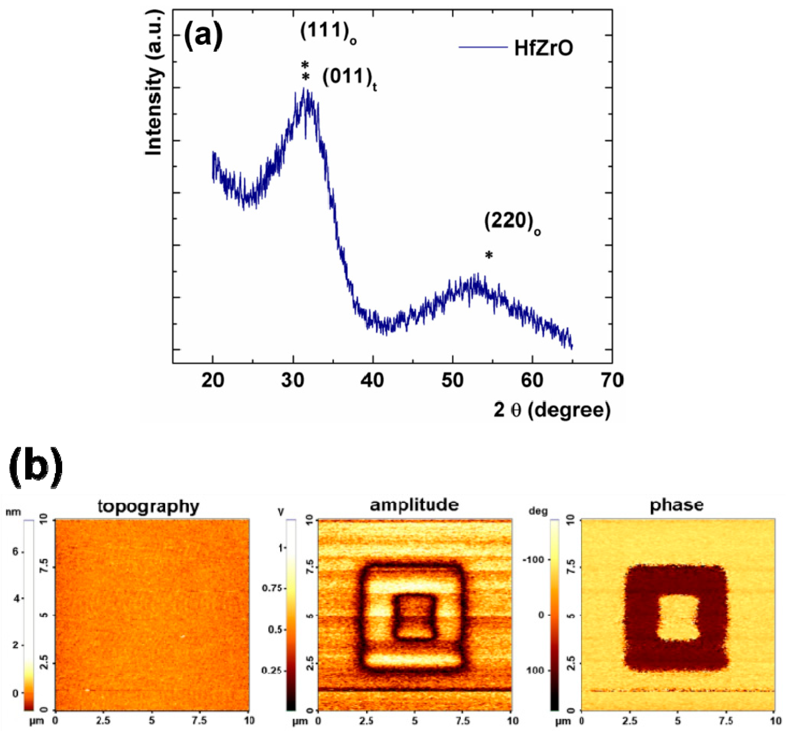
Grazing incidence X-ray diffraction (GIXRD) and piezo-response force microscopy (PFM) measurements were used in order to validate the ferroelectricity of the HfZrO thin film. GIXRD measurements were performed while using a high-resolution X-ray diffractometer that employs Cu Kα1 radiation (λ = 1.54 Å). The incidence angle was set to 0.35 degrees. Figure 2a shows the GIXRD spectra of the HfZrO thin film in the wide 2θ range of 20–65°, and indicates the coexistence of several phases in Zr-doped HfO2 thin films. Due to the polycrystalline nature of HfZrO layers deposited by the ALD technique, the mixed composition of orientations and phases, as well as the very small films thickness up to ~10 nm, the structural analysis of HfZrO thin films is not an easy task. In addition, even the GIXRD measurements cannot clearly distinguish between the orthorhombic and tetragonal structures of HfO2 due to the structural similarities of the orthorhombic and tetragonal phases (similarities in their lattice structures) [5]. The most intense diffraction peak is assigned as the mixture of (011) of the t-phase and (111) of the o-phase, formed by the presence of overlapping reflections that are associated with the tetragonal (P42/nmc) and the orthorhombic polar phase (Pca21) [6]. The formation of the orthorhombic polar phase in Zr-doped HfO2 thin films is confirmed by the presence of the two diffraction peaks near 2θ = 30.5° and 55° assigned to (111)o and (220)o reflections. The GIXRD spectrum also indicates an inhibition of m-phase HfO2 that was induced by Zr doping, by presence of the significantly lower monoclinic (111)m reflections, expected around 28° at 2θ angle. The inhibition of the monoclinic reflections and the presence of the orthorhombic polar and tetragonal phases indicate that the film has a polycrystalline structure in which the ferroelectric phase is dominant [15]. The absence of peaks due to the Si substrate, in GXRD measurement, can be obtained by changing the orientation of the silicon wafer in the X-ray field, so the signal on the Si substrate is suppressed. PFM measurements were also carried out on the HfZrO thin films to further demonstrate ferroelectricity. For the manipulation of the ferroelectric domains, the atomic force microscopy (AFM) tip was held at 0 V and a DC bias between −10 V and 10 V was applied to the substrate during scanning. The local mechanical response was determined by applying an alternating current (AC) bias to the AFM tip, while the substrate was held at 0 V. Figure 2b displays the topography image together with the corresponding images of the amplitude and phase signals, which show the intensity of the local mechanical response, and the phase shift between the response and the excitation, respectively. The PFM measurements demonstrate that the HfZrO film exhibits an easy switching of polarization along the poling direction, with clear boundaries between upward and downward domains being observed in phase and amplitude images. The phase shift differs by approximately 180° between the successively written areas, showing that the fabricated HfZrO thin film is indeed ferroelectric.
In addition to PFM investigations, average roughness measurements were performed on 2 μm × 2 μm areas. The average roughness was found to be 0.2 nm for HfZrO films with a thickness of 6 nm. The uniform topography, without holes, and the low surface roughness, give information about the composition and structure of the film, which are relatively constant in volume [16].
Perhaps the most recognizable electrical characterization of a ferroelectric is the hysteresis loop. In order to test the ferroelectric behaviour of the HfZrO thin film, we obtained the polarization versus voltage (P–V) loop. During the initial electric field cycling, the remanent polarization (Pr) was found at ~0.8 μC/cm2 and the coercive voltage at ~2.6 V. A well-known phenomenon in ferroelectrics is the wake-up effect, which does not appear in the case when HfZrO is grown directly on Si (as in our case) even if the HfZrO has a thickness of 1 nm [17].
We stress here that the ferroelectric phase is assigned to the orthorhombic polar phase (o-phase) corresponding to the Pca21 space group [18], but other phases are generally present inside the hafnium oxide after the growth process, due to stabilization problems. At room temperature, the stable form of the HfO2-based compounds is a monoclinic phase (P21/c, m-phase), whereas, at high-temperatures and pressures, the tetragonal (P42/nmc, t-phase) and the cubic (Fm3m, c-phase) phases are dominant [19]. Nevertheless, for hafnium oxide films up to 10–15 nm in thickness, the transition temperatures of the monoclinic to the tetragonal phase are significantly lowered [20]. In addition, the tetragonal and cubic phases can be stabilized at room temperature via doping [21]. Since 2011, when ferroelectricity in Si-doped HfO2 thin films was first reported [5], it has been shown that many other dopants, such as Y, Al, Zr, Gd, Yb, Sr, and La, can induce ferroelectricity in the HfO2 thin films [22]. Through a suitable combination of doping, stress and/or electric field the tetragonal P42/nmc phase can make a transition into the polar orthorhombic Pca21 phase [23]. Moreover, a remarkable feature is that, as the thickness increases (>10 nm), the ferroelectricity in HfO2-based compounds disappears. Hf-based ferroelectrics only have nanoscale ferroelectricity, where other ferroelectrics lose it [24].
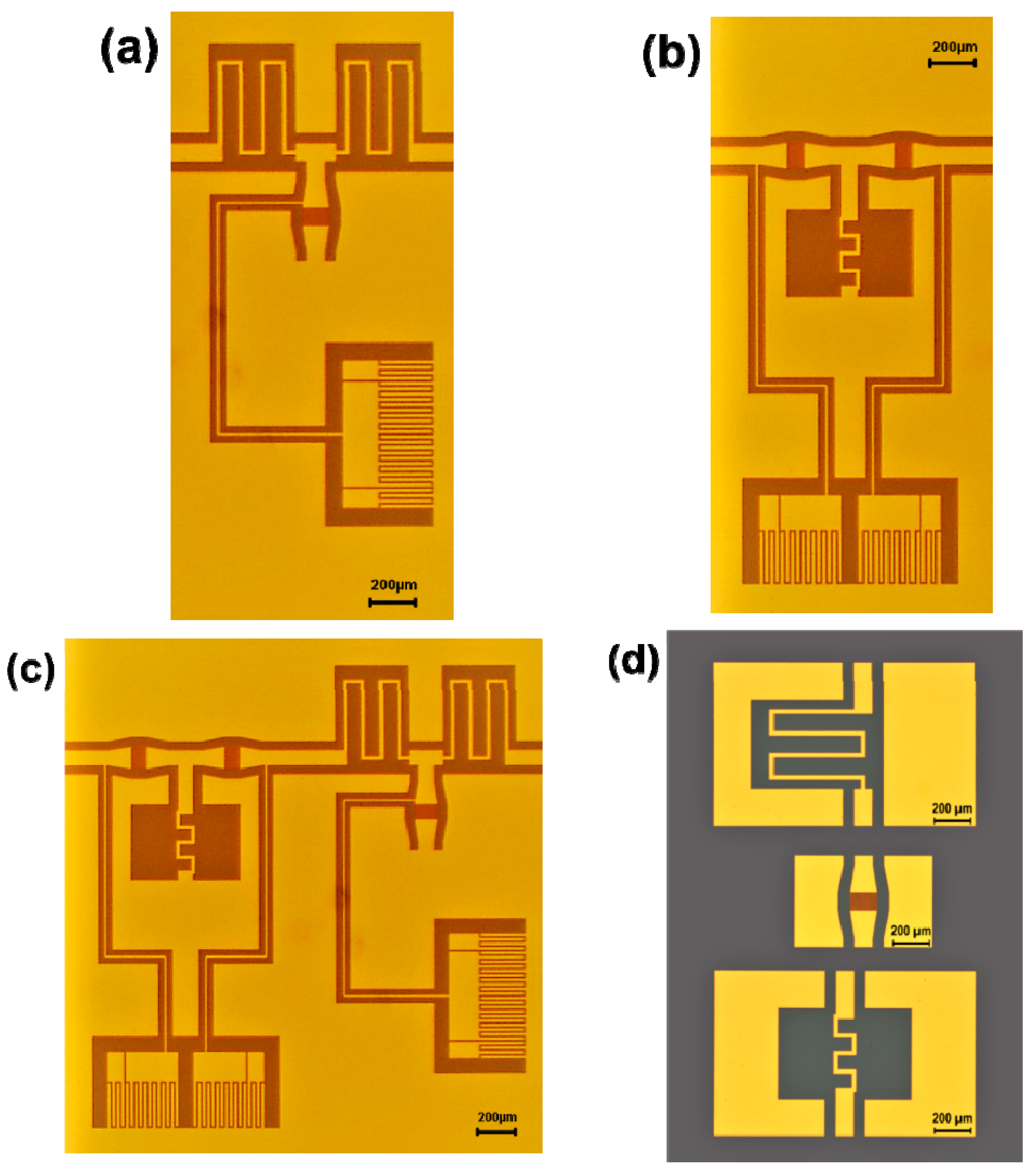
The proposed ferroelectric filter needs fulfill some basic requirements: (i) low-voltage tunability; (ii) CMOS compatibility; (iii) compact dimensions; and, (iv) ease of fabrication, as mentioned in the Introduction. Moreover, a reconfigurability is envisaged to switch among the low-pass, the high-pass and the band-pass topologies. We describe the strategies adopted for each of the above constraints hereinafter. For the low-voltage tunability, as discussed in the Introduction we exploited the ferroelectric properties of HfZrO, which also confer CMOS compatibility and ease of integration, as a single mask is required to deposit the metal layer onto the HRSi/HfZrO substrate. The filters’ key sub-components are the inductors and the IDCs, with the latter working as variable capacitors (varactors) due to the underneath ferroelectric layer. For the reconfigurability, we chose to implement a BPF made of an LPF in series with an HPF. Between them, Single Pole Double Throw (SPDT) switches (to be integrated in the future) will allow the reconfiguration by selecting the desired filter (i.e., the appropriate input-output ports). The last requirement, perhaps the most critical one, is represented by the compact dimensions. For this purpose, the adopted strategy was to start with an equivalent circuit model (using AWR Microwave Office®) for each of the three filters and based on lumped elements. The next step was the translation of the three circuits into their 3D EM versions in CPW technology for ease of integration in order to take all the potential parasitic effects and EM couplings occurring in microwaves up to 20 GHz into account (using CST Microwave Studio®). Each basic filter (LPF and HPF) was implemented by a T-network; then, as already stated, the BPF was formed by connecting the LPF (made by two series inductances and a shunt varactor) to the HPF (made by two series varactors and a shunt inductor). As a major result, the BPF has much lower dimensions (3.19 mm × 3.47 mm) than the working wavelength. The optical images of the fabricated filters and the test structures are shown in Figure 3a–d. One can clearly distinguish the architectures of the three filters in Figure 3a–c, which are made of sub-components in CPW technology for ease-of-embedding in integrated circuits. One can also notice big interdigital adjustable capacitors for independent DC bias of the varactors, RF-decoupled by λg/4-long lines (λg is the guided wavelength at 10 GHz, i.e., the reference central frequency for the BPF). These capacitors have a capacitance of about 1 pF for the LPF and 0.3 pF for the HPF. Figure 3d displays the test structures of the filters’ key sub-components, i.e., the inductor for the LPF, the IDC, and the inductor for the HPF. In detail, the two series inductors of the LPF have a theoretical inductance of 0.79 nH, whereas the shunt inductor of the HPF has a theoretical inductance of 0.3 nH, in order to have the desired band-pass filtering in the X band (8.2–12.4 GHz). The gold has a thickness of 360 nm. Each IDC has 30 digits, which are 100 μm long and 2.5 μm wide, with a spacing of 2.5 μm between two adjacent digits. The overall IDC is only 147.5 μm wide.
3. Results and Discussion
The microwave measurements were made on-wafer at room temperature using a vector network analyser (VNA) Anritsu-37397D connected to a Karl-Süss PM5 probe station. The DC bias was provided by a DC source and the above mentioned big interdigital adjustable capacitors, in order to separate the DC bias from the high-frequency excitation signal.
3.1. Extraction of Relative Permittivity and Microwave Characteristics of HfZrO-Based IDCs
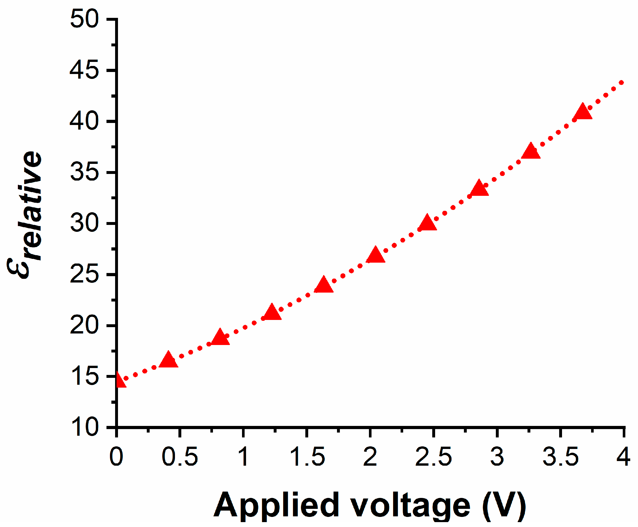
The extracted curve for ε(V) at 10 GHz using Equations (1) and (2) is shown in Figure 4, which was obtained by means of the Bianco–Parodi method described in [10] applied to two CPW lines of different lengths, designed on a HRSi/HfZrO substrate, and fabricated in the same run together with the structures that are presented in this work. Hence, this figure represents the value of the bias-dependent permittivity of HfZrO at a specific frequency, irrespective of the microwave device making use of a ferroelectric HfZrO thin film.
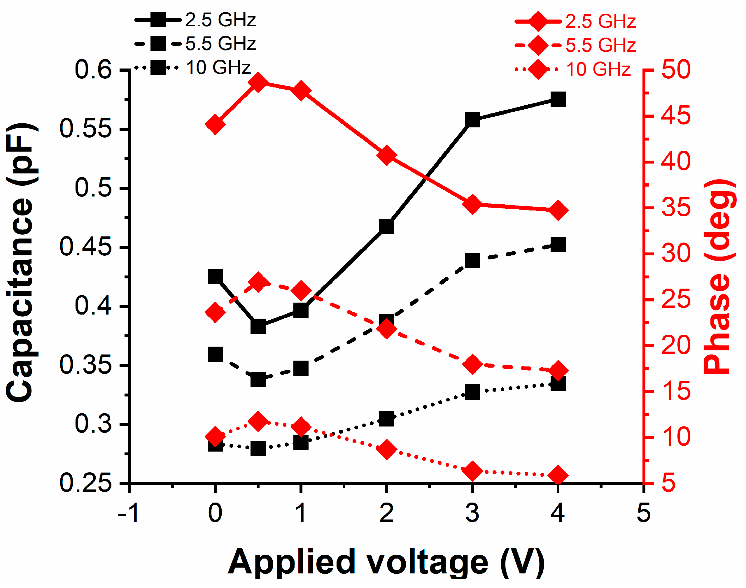
Figure 5 displays the measurements for a single IDC in CPW configuration in terms of its capacitance CIDC and phase ϕIDC (the latter as extracted from the transmission parameter |S21| or |S12|, which gives the proof in microwaves of the ferroelectricity of HfZrO) for three reference frequencies, i.e., 2.5 GHz and 5.5 GHz (associated to ISM—industrial, scientific, and medical—applications), and 10 GHz. We see that, at the frequency of 2.5 GHz, the sweeping of the DC voltage from 0.5 V up to 4 V increases the capacitance from 0.38 pF to 0.58 pF, whereas the phase decreases from 48.7° to 34.7°, i.e., a phase shift of 14°. Increasing the frequency to 10 GHz and sweeping the DC voltage in the same range, the capacitance increases from 0.28 pF to 0.33 pF, while the phase decreases from 11.76° to 5.86°, i.e., a phase shift of about 6°. This trend for CIDC and ϕIDC is consistent with the ferroelectric nature of the HfZrO thin film: when applying an external DC electric field Ea, the hysteric behaviour of the relative permittivity ε is such that it reaches its maximum εmax for Ea,max ≠ 0 V/m [14] or, equivalently, for an applied DC bias voltage Vmax ≠ 0 V. In the case of HfZrO, εmax ≈ 60 at Vmax ≈ ±5 V. At the same time, the estimation of the capacitance of an IDC structure on a multi-layer substrate is quite cumbersome from a mathematical point of view, but, as expected, an increase of relative permittivity leads to an increase of the overall capacitance [25,26]. Also, the relation between CIDC and ϕIDC is of the type ϕIDC = arctg(1/ωCIDC) (where ω is the angular frequency); hence, an increase of the capacitance with the DC bias corresponds to a decrease of the phase. Table 1 summarises the main variations of CIDC, RIDC (extracted IDC’s resistance) and ϕIDC at frequencies of interest. From Table 1 one can notice that CIDC can be increased for each frequency between 20% and 53% (with respect to its minimum value at 0.5 V), the results for the symmetric case—negative bias values—being very similar; this represents the key of the tunability characteristics of the proposed filter. At the same time, losses also increase with the DC bias (due to the increase of RIDC), which entails a higher insertion loss. However, as demonstrated in [10], the effective loss tangent of a 6-nm-thick HfZrO thin film decreases with frequency (and increases with bias). Nevertheless, it exhibits small variations with the applied DC voltage, which entails a lowering of the dielectric losses in the ferroelectric. Furthermore, a reduction of the skin depth is observed in metals when increasing the frequency, which also decreases the overall power losses of the EM waves that propagate along the single IDC. Possible countermeasures to reduce RIDC could be: (i) increase of the number of digits (using Electron Beam Lithography techniques); and, (ii) increase of gold thickness. These issues will be investigated in successive fabrication batches, as a trade-off between CIDC and RIDC is needed. Besides this, it is worth noting that a peculiar characteristic of any ferroelectric is its hysteretic nature. From the microwave point of view, when measuring the phase of the single IDC in the band of interest, the curve does not follow the same path when decreasing (or changing the polarity of) the applied DC voltage. In detail, when returning from ±4 V to 0 V, the reference (initial) state at 0 V was not re-established exactly or, in other words, a (temporary) change of the initial state has to be taken into account, together with a discharge process (with a recovery time in the order of a couple of minutes) that is necessary to re-align the ferroelectric dipoles in the unbiased situation.
3.2. Microwave Measurements of the Three HfZrO-Based Filters
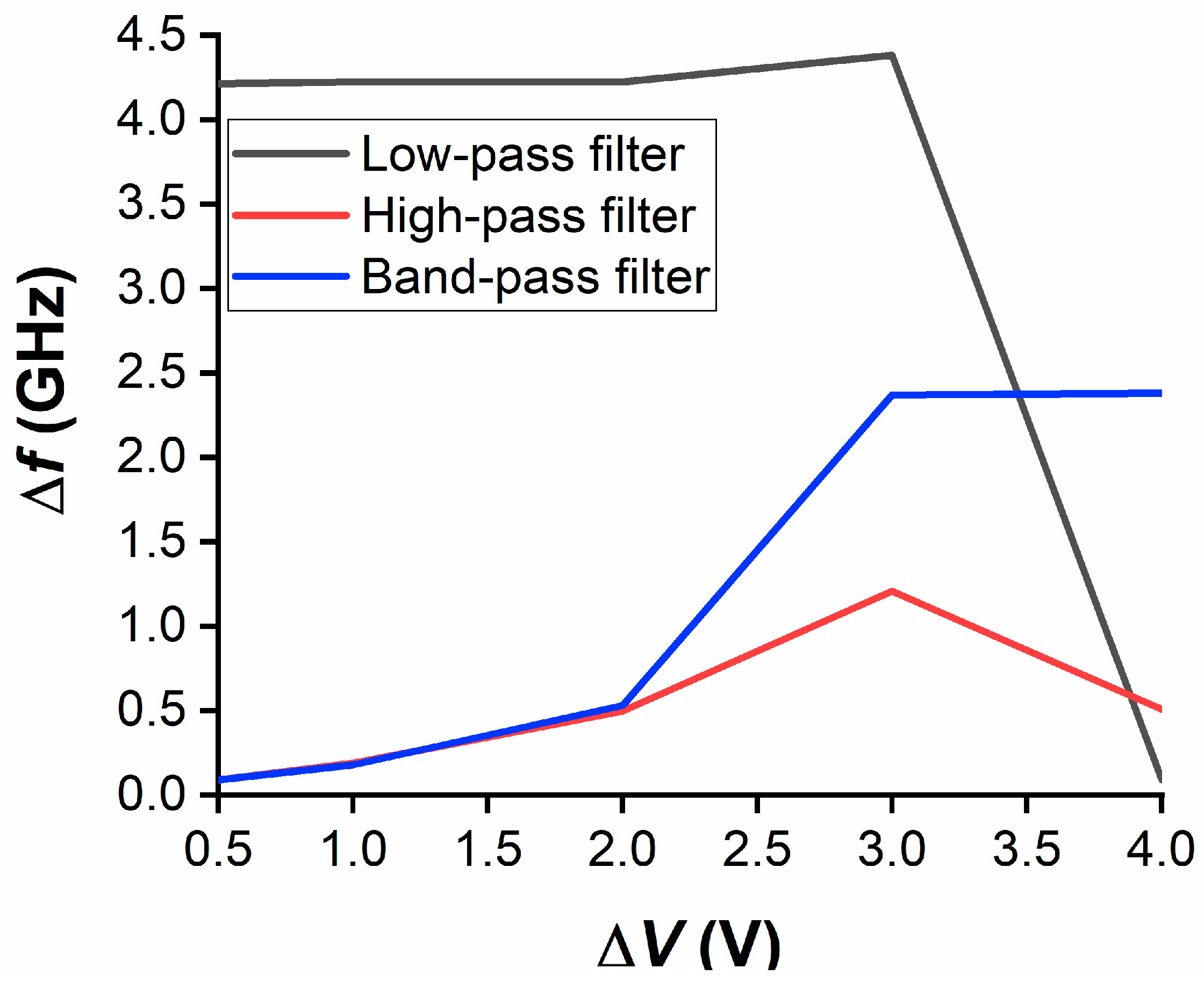
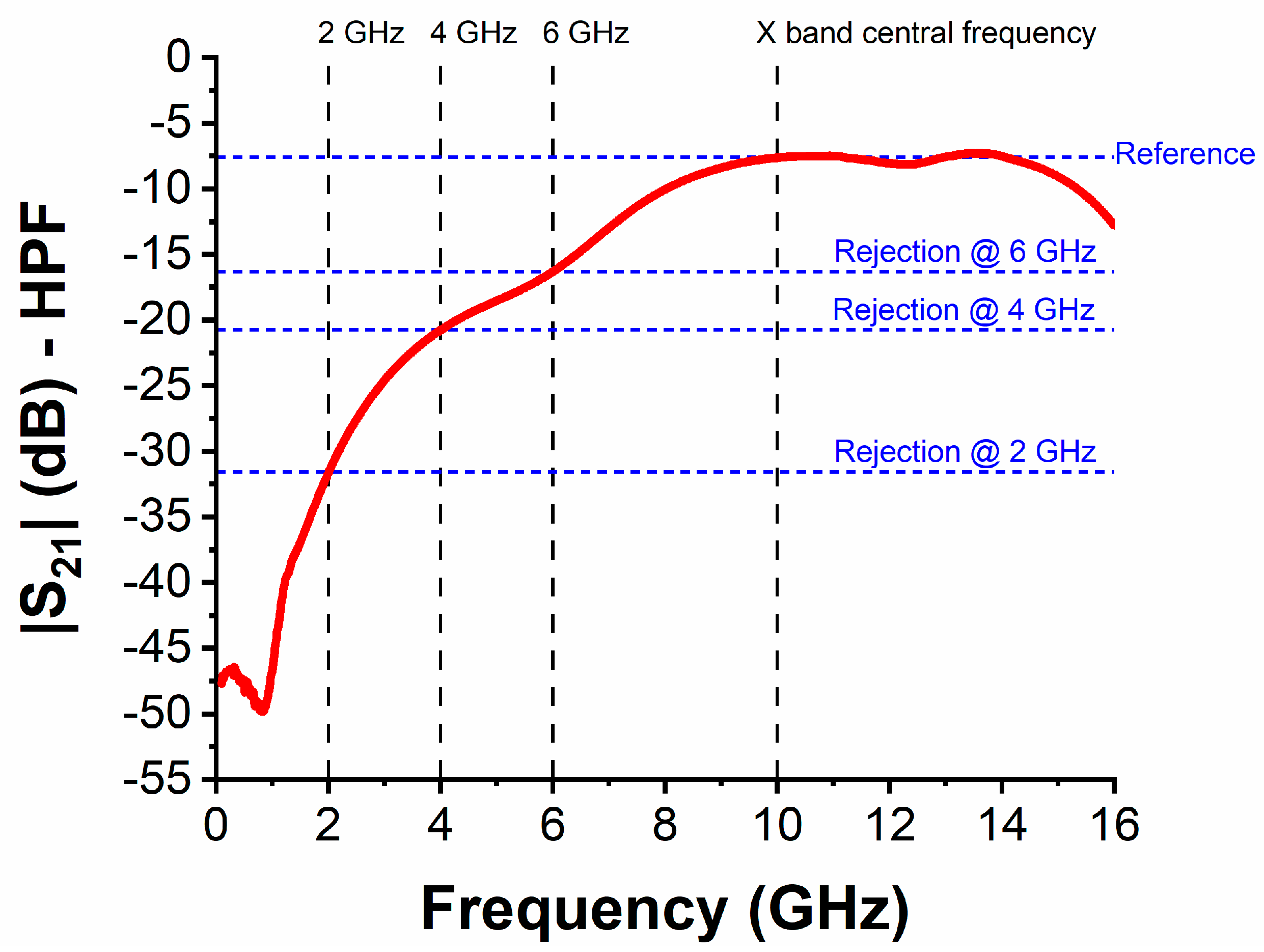
Finally, the three filters were measured in the frequency range 0.1–16 GHz. Here, we stress that all three filters are deeply sub-wavelength (with overall dimension of about λ0/20 × λ0/10 for LPF and HPF, and of about λ0/9 × λ0/9 for BPF—where λ0 is the free-space wavelength at 10 GHz), which means that they exhibit higher losses than off-the-shelf bulk components or, in other words, miniaturized filters have the drawback of high losses which often require a post-amplification stage. Table 2 summarises the main performance for each one of the three filters in terms of |S11| and |S21|, whereas Figure 6 displays the frequency shift Δf (in GHz) for |S11| of each filter in its reference band, as a function of the voltage difference ΔV = Vi − Vunbiased (in volts), where i = 1, 2, 3, 4, 5 and Vunbiased = 0 V (unbiased case). The reference band is calculated when considering the frequency range in which |S11| is less than (or equal to) −6 dB, whereas the insertion loss (IL) is calculated as IL (dB) = −log10|S21|. The reference band for each filter was expected to cover partially (LPF) or entirely (HPF and BPF) the X band and, as one can notice from Table 2, this requirement is fully complied with. Table 2 also shows the minimum value of |S11| in the reference band and the best value of the IL in the X band (ILBEST,X band). The IL exhibits high values due to the lossy nature of the three filters (as discussed before), especially for the BPF. Nevertheless, in the case of the BPF, the X band maximum rejection (defined as the difference between the maximum value of the IL and the IL at the edges of the X band, i.e., at 8.2 and 12.4 GHz) has a rather good value of more than 10.8 dB. Regarding Figure 6, it shows that the frequency shift for |S11| reaches almost 4.5 GHz at 3 V for the LPF, more than 1 GHz at 3 V for the HPF and more than 2.5 GHz at 4 V for the BPF. This frequency shift is the main effect that is given by the HfZrO ferroelectric thin film, since a change of maximum 8% of the effective permittivity (equivalent to a change of about 65% of the relative permittivity) allows for changing the phase of the microwave signal when passing through the filter (together with a moderate change of the characteristic impedance at filter’s ports, hence slightly improving or decreasing the matching to 50 Ω). When considering the performance of the three filters in terms of |S21| (|S12|), the most significant results were obtained for the HPF. In Figure 7, we show the transmission coefficient at 3 V (to which corresponds the maximum value of Δf for the HPF in Figure 6, solid red curve): in this case, the rejection with respect to the central frequency in the X band (i.e., 10 GHz) is about 8.7 dB at 6 GHz, 13.2 dB at 4 GHz, and 24 dB at 2 GHz. Taking the previous discussion about the losses in the filter into account, it was expected to not have excellent values of steepness and rejection; these issues being presently under study in successive fabrication batches, including different dopants besides Zr.
4. Conclusions
In this paper, we have presented three ferroelectric-based microwave filters with low-voltage tunable characteristics, which allow for controlling the frequency shift of the reflection coefficient and the insertion loss in a wide frequency range, covering the band from 0.1 GHz up to 16 GHz. First, a simple yet effective mathematical relation has been derived in order to accurately predict the voltage-dependent behaviour of the relative permittivity of HfZrO ferroelectric thin films at a desired frequency, while taking its geometrical and physical characteristics into account. Subsequently, the fabricated 6-nm-thick HfZrO ferroelectric layer has been exploited for the design, fabrication, and experimental verification of a low-pass, a high-pass, and a band-pass filter embedding HfZrO-based varactors. In spite of the low value of the maximum DC bias applied (i.e., not exceeding 4 V), very promising tuning properties have been observed for all the filters under test, with a maximum frequency shift of almost 4.5 GHz at 3 V for the low-pass filter. These results further open the path towards low-voltage CMOS-compatible ferroelectric-based electronics, which are suitable for next-generation wireless applications.
Author Contributions
Conceptualization, M.A., M.D., S.I.; Fabrication, F.N., S.V.; Methodology, M.A., M.D., S.I., F.N.; Measurements, M.A., S.I., F.N.; Data curation, M.A., S.I., F.N.; Formal analysis, M.A., M.D., S.I., F.N.; Funding acquisition, M.D.; Project administration, M.D.; Supervision, M.D.; Validation, M.A., M.D., S.I., F.N.; Writing—Original draft, M.A., M.D., S.I., F.N. All authors have read and agreed to the published version of the manuscript.
Funding
The authors acknowledge the support from the European Project “NANOSMART”, ICT-07-2018_RIA, proposal number: SEP-210506362, and from the GRAPHENEFERRO grant of UEFISCDI, under Project PN-III-P4-ID-PCCF-2016-0033.
Conflicts of Interest
The authors declare no conflict of interest.
References
- Kita, K.; Kyuno, K.; Toriumi, A. Permittivity increase of yttrium-doped HfO2 through structural phase transformation. Appl. Phys. Lett. 2005, 86, 102906. [Google Scholar] [CrossRef]
- Tomida, K.; Kita, K.; Toriumi, A. Dielectric constant enhancement due to Si incorporation into HfO2. Appl. Phys. Lett. 2006, 89, 142902. [Google Scholar] [CrossRef]
- Bang, S.; Lee, S.; Jeon, S.; Kwon, S.; Jeong, W.; Kim, S.; Jeon, H. Physical and electrical properties of hafnium–zirconium–oxide films grown by atomic layer deposition. J. Electrochem. Soc. 2008, 155, H633. [Google Scholar] [CrossRef]
- Böscke, T.S.; Hung, P.Y.; Kirsch, P.D.; Quevedo-Lopez, M.A.; Ramírez-Bon, R. Increasing permittivity in HfZrO thin films by surface manipulation. Appl. Phys. Lett. 2009, 95, 052904. [Google Scholar] [CrossRef]
- Böscke, T.S.; Müller, J.; Bräuhaus, D.; Schröder, U.; Böttger, U. Ferroelectricity in hafnium oxide thin films. Appl. Phys. Lett. 2011, 99, 102903. [Google Scholar] [CrossRef]
- Müller, J.; Böscke, T.S.; Schröder, U.; Mueller, S.; Braühaus, D.; Böttger, U.; Frey, L.; Mikolajick, T. Ferroelectricity in simple binary ZrO2 and HfO2. Nano Lett. 2012, 12, 4318–4323. [Google Scholar] [CrossRef] [PubMed]
- Fischer, D.; Kersch, A. The effect of dopants on the dielectric constant of HfO and ZrO from first principles. Appl. Phys. Lett. 2008, 92, 012908. [Google Scholar] [CrossRef]
- Park, M.H.; Lee, Y.H.; Kim, H.J.; Kim, Y.J.; Moon, T.; Kim, K.D.; Müller, J.; Kersch, A.; Schroeder, U.; Mikolajick, T.; et al. Ferroelectricity and antiferroelectricity of doped thin HfO2-Based Films. Adv. Mater. 2015, 27, 1811–1831. [Google Scholar] [CrossRef] [PubMed]
- Ahmed, A.; Goldhorpe, I.A.; Khandani, A.K. Electrically tunable materials for microwave applications. Appl. Phys. Rev. 2015, 2, 011302. [Google Scholar] [CrossRef]
- Aldrigo, M.; Dragoman, M.; Iordanescu, S.; Nastase, F.; Vulpe, S.; Dinescu, A.; Vasilache, D. Low-voltage permittivity control of coplanar lines based on hafnium oxide ferroelectrics grown on silicon. IEEE Access 2019, 7, 136686–136693. [Google Scholar] [CrossRef]
- Zhu, L.; Sun, S.; Li, R. Microwave Bandpass Filters for Wideband Communications; John Wiley & Sons Inc.: Hoboken, NJ, USA, 2012. [Google Scholar]
- Aldrigo, M.; Dragoman, M.; Laudadio, E.; Iordanescu, S.; Modreanu, M.; Povey, I.M.; Nastase, F.; Vulpe, S.; Stipa, P.; Di Donato, A.; et al. Microwave applications of zirconium-doped hafnium oxide ferroelectrics: From nanoscale calculations up to experimental results. In Proceedings of the 2020 IEEE/MTT-S International Microwave Symposium (IMS), Los Angeles, CA, USA, 4–6 August 2020; pp. 520–523. [Google Scholar]
- Chernikova, A.; Kozodaev, M.; Markeev, A.; Negrov, D.; Spiridonov, M.; Zarubin, S.; Bak, O.; Buragohain, P.; Lu, H.; Suvorova, E.; et al. Ultrathin Hf0.5Zr0.5O2 ferroelectric films on Si. ACS Appl. Mater. Interfaces 2016, 8, 7232–7237. [Google Scholar] [CrossRef] [PubMed]
- Placeres-Jiménez, R.; Rino, J.P.; Eiras, J.A. Modeling ferroelectric permittivity dependence on electric field and estimation of the intrinsic and extrinsic contributions. J. Phys. D Appl. Phys. 2015, 48, 035304. [Google Scholar]
- Lederer, M.; Kämpfe, T.; Vogel, N.; Utess, D.; Volkmann, B.; Ali, T.; Olivo, R.; Müller, J.; Beyer, S.; Trentzsch, M.; et al. Structural and electrical comparison of Si and Zr doped hafnium oxide thin films and integrated FeFETs utilizing transmission Kikuchi diffraction. Nanomaterials 2020, 10, 384. [Google Scholar] [CrossRef] [PubMed] [Green Version]
- Hausmann, D.M.; Gordon, R.G. Surface morphology and crystallinity control in the atomic layer deposition (ALD) of hafnium and zirconium oxide thin films. J. Cryst. Growth 2003, 249, 251–261. [Google Scholar] [CrossRef]
- Cheema, S.S.; Kwon, D.; Shanker, N.; dos Reis, R.; Hsu, S.-H.; Xiao, J.; Zhang, H.; Wagner, R.; Datar, A.; McCarter, M.R.; et al. Enhanced ferroelectricity in ultrathin films grown directly on silicon. Nature 2020, 580, 478–482. [Google Scholar] [CrossRef] [PubMed]
- Sang, X.; Grimley, E.D.; Schenk, T.; Schroeder, U.; LeBeau, J.M. On the structural origins of ferroelectricity in HfO2 thin films. Appl. Phys. Lett. 2015, 106, 162905. [Google Scholar] [CrossRef]
- Ohtaka, O.; Fukui, H.; Kunisada, T.; Fujisawa, T.; Funakoshi, K.; Utsumi, W.; Irifune, T.; Kuroda, K.; Kikegawa, T. Phase relations and volume changes of hafnia under high pressure and high temperature. J. Am. Ceram. Soc. 2001, 84, 1369–1373. [Google Scholar] [CrossRef]
- Park, M.H.; Schenk, T.; Fancher, C.M.; Grimley, E.D.; Zhou, C.; Richter, C.; LeBeau, J.M.; Jones, J.L.; Mikolajick, T.; Schroeder, U. A comprehensive study on the structural evolution of HfO2 thin films doped with various dopants. J. Mater. Chem. C 2017, 5, 4677–4690. [Google Scholar] [CrossRef]
- Lee, C.-K.; Cho, E.; Lee, H.-S.; Hwang, C.S.; Han, S. First-principles study on doping and phase stability of HfO2. Phys. Rev. B 2008, 78, 012102. [Google Scholar] [CrossRef]
- Müller, J.; Polakowski, P.; Riedel, S.; Mueller, S.; Yurchuk, E.; Mikolajick, T. Ferroelectric hafnium oxide a game changer to FRAM? In Proceedings of the 14th Annual Non-Volatile Memory Technology Symposium (NVMTS), Jeju Island, Korea, 27–29 October 2014; pp. 1–7. [Google Scholar]
- Huan, T.D.; Sharma, V.; Rossetti, G.A., Jr.; Ramprasad, R. Pathways towards ferroelectricity in hafnia. Phys. Rev. B 2014, 90, 064111. [Google Scholar] [CrossRef] [Green Version]
- Schroeder, U.; Hwang, C.S.; Funakubo, H. Ferroelectricity in Doped Hafnium Oxide: Materials, Properties and Devices; Woodhead Publishing Series in Electronic and Optical Materials; Woodhead Publishing: Duxford, UK, 2019. [Google Scholar]
- Igreja, R.; Dias, C.J. Analytical evaluation of the interdigital electrodes capacitance for a multi-layered structure. Sens. Actuators A 2004, 112, 291–301. [Google Scholar] [CrossRef]
- Igreja, R.; Dias, C.J. Extension to the analytical model of the interdigital electrodes capacitance for a multi-layered structure. Sens. Actuators A 2011, 172, 392–399. [Google Scholar] [CrossRef]
Figure 1.
Energy-dispersive X-ray (EDX) analysis spectra of the 6-nm-thick HfZrO film.

Figure 2.
(a) Grazing incidence X-ray diffraction (GIXRD) spectra and (b) piezo-response force microscopy (PFM) topography (left), amplitude (centre), and phase (right) of the 6-nm-thick HfZrO film.
Figure 2.
(a) Grazing incidence X-ray diffraction (GIXRD) spectra and (b) piezo-response force microscopy (PFM) topography (left), amplitude (centre), and phase (right) of the 6-nm-thick HfZrO film.

Figure 3.
Optical pictures of the (a) low-pass filter, (b) high-pass filter, and (c) band-pass filter; and, (d) optical picture of the test structures. From top to down: inductor for low-pass filter, interdigital capacitor and inductor for high-pass filter.
Figure 3.
Optical pictures of the (a) low-pass filter, (b) high-pass filter, and (c) band-pass filter; and, (d) optical picture of the test structures. From top to down: inductor for low-pass filter, interdigital capacitor and inductor for high-pass filter.

Figure 4.
Extracted relative permittivity of the 6-nm-thick HfZrO ferroelectric at 10 GHz, as a function of the applied DC bias voltage in the range 0–4 V.
Figure 4.
Extracted relative permittivity of the 6-nm-thick HfZrO ferroelectric at 10 GHz, as a function of the applied DC bias voltage in the range 0–4 V.

Figure 5.
Measured capacitance (left vertical axis) and phase (right vertical axis) of the single interdigital capacitor at three reference frequencies (2.5 GHz, 5.5 GHz, and 10 GHz) for an applied DC bias voltage in the range 0–4 V.
Figure 5.
Measured capacitance (left vertical axis) and phase (right vertical axis) of the single interdigital capacitor at three reference frequencies (2.5 GHz, 5.5 GHz, and 10 GHz) for an applied DC bias voltage in the range 0–4 V.

Figure 6.
Frequency shift of the reflection coefficient |S11| for the three filters in the reference band, as a function of the applied DC bias voltage.
Figure 6.
Frequency shift of the reflection coefficient |S11| for the three filters in the reference band, as a function of the applied DC bias voltage.

Figure 7.
Transmission coefficient |S21| for the HPF at 3 V. The reference frequencies and values of |S21| are highlighted for an estimation at a glance of filter’s rejection properties.
Figure 7.
Transmission coefficient |S21| for the HPF at 3 V. The reference frequencies and values of |S21| are highlighted for an estimation at a glance of filter’s rejection properties.


Table 1.
Values of CIDC (pF), RIDC (Ω), and ϕIDC (deg) at different frequencies for two values of the DC bias voltage.
Table 1.
Values of CIDC (pF), RIDC (Ω), and ϕIDC (deg) at different frequencies for two values of the DC bias voltage.
| Frequency (GHz) | CIDC (pF) | RIDC (Ω) | ϕIDC (deg) | |||
|---|---|---|---|---|---|---|
| 0.5 V | 4 V | 0.5 V | 4 V | 0.5 V | 4 V | |
| 2.5 | 0.38 | 0.58 | 76.43 | 85.53 | 48.69 | 34.76 |
| 5.5 | 0.34 | 0.45 | 65.69 | 73.13 | 26.94 | 17.29 |
| 8 | 0.30 | 0.38 | 59.51 | 65.70 | 17.27 | 10.14 |
| 10 | 0.28 | 0.33 | 55.2 | 60.46 | 11.76 | 5.86 |
| 12 | 0.26 | 0.31 | 51.67 | 56.19 | 7.05 | 2.05 |
Table 2.
Main performance of the three filters in terms of reference band, minimum value of |S11| in the reference band, and best value of the insertion loss in the X band.
Table 2.
Main performance of the three filters in terms of reference band, minimum value of |S11| in the reference band, and best value of the insertion loss in the X band.
| Filter Type | Reference Band | |S11|min | ILBEST,X band |
|---|---|---|---|
| Low-Pass | 0.1–10.5 GHz | −22.8 dB | 9.1 dB |
| High-Pass | 4.13–16 GHz | −18.3 dB | 7.5 dB |
| Band-Pass | 4.6–15 GHz | −18.7 dB | 14.7 dB |
Publisher’s Note: MDPI stays neutral with regard to jurisdictional claims in published maps and institutional affiliations. |
© 2020 by the authors. Licensee MDPI, Basel, Switzerland. This article is an open access article distributed under the terms and conditions of the Creative Commons Attribution (CC BY) license (http://creativecommons.org/licenses/by/4.0/).
Share and Cite
MDPI and ACS Style
Aldrigo, M.; Dragoman, M.; Iordanescu, S.; Nastase, F.; Vulpe, S. Tunable Microwave Filters Using HfO2-Based Ferroelectrics. Nanomaterials 2020, 10, 2057. https://doi.org/10.3390/nano10102057
AMA Style
Aldrigo M, Dragoman M, Iordanescu S, Nastase F, Vulpe S. Tunable Microwave Filters Using HfO2-Based Ferroelectrics. Nanomaterials. 2020; 10(10):2057. https://doi.org/10.3390/nano10102057
Chicago/Turabian StyleAldrigo, Martino, Mircea Dragoman, Sergiu Iordanescu, Florin Nastase, and Silviu Vulpe. 2020. "Tunable Microwave Filters Using HfO2-Based Ferroelectrics" Nanomaterials 10, no. 10: 2057. https://doi.org/10.3390/nano10102057
Note that from the first issue of 2016, this journal uses article numbers instead of page numbers. See further details here.