Communication

Channel Structures Formed in Copper Ingots upon Melting and Evaporation by a High-Power Electron Beam

1
Khristianovich Institute of Applied and Theoretical Mechanics, Siberian Branch of the Russian Academy of Sciences, Institutskaya str., 4/1, Novosibirsk 630090, Russia
2
Department of Physics and Engineering, Buryat State University, Smolina str., 24a, Ulan-Ude 670000, Russia
3
Institute of Physical Materials, Siberian Branch of the Russian Academy of Sciences, Sakhyanovoy str., 6, Ulan-Ude 670047, Russia
4
Budker Institute of Nuclear Physics, Siberian Branch of the Russian Academy of Sciences, Lavrenteva str., 11, Novosibirsk 630090, Russia
5
Department of Physics, Novosibirsk State University, Pirogova str., 20, Novosibirsk 630090, Russia
*
Author to whom correspondence should be addressed.
Metals 2015, 5(1), 428-438; https://doi.org/10.3390/met5010428
Submission received: 5 November 2014 / Revised: 12 February 2015 / Accepted: 5 March 2015 / Published: 12 March 2015

Abstract

:
A new phenomenon is described in this paper: the formation of macroscopic channel structures on the bottom of copper ingots which were used as the target for the synthesis of copper nanoparticles by high-power electron beam evaporation and condensation. In the synthesis experiment, the cylindrical copper ingot is melted and partially evaporated in a graphite crucible. The channel structures were originally observed after a series of nanoparticle synthesis experiments in varying conditions. In the present work, various process conditions are varied in order to recreate the structures and identify their mechanism of formation. Conditions in which the channel structures form and do not form are identified and interesting microstructures are observed near the channel structures.

1. Introduction

For more than 20 years, the Khristianovich Institute of Applied and Theoretical Mechanics (KITAM) has been working in collaboration with the Budker Institute of Nuclear Physics (BINP), both institutes part of the Siberian Branch of the Russian Academy of Sciences (SB RAS), in order to obtain nanopowders from various substances by evaporating the materials using an electron beam [1,2,3]. The electron beam is generated by a high-voltage ELV type accelerator [4]. The beam has an energy of 1.4 MeV and can have as high as a 100 kW output into the atmosphere through a diaphragm with a diameter of about 1–2 mm. In the synthesis experiments, the beam travels half a dozen centimeters into a chamber with a gas flowing at close to atmospheric pressure along the target material surface. The beam then melts and evaporates the target material to produce a vapor which is subsequently condensed into nanoparticles. The phenomenon described in the current paper was discovered after one cycle of studies to obtain copper nanopowders in an argon atmosphere through the electron beam evaporation technique. The details of the copper nanoparticles synthesized can be found in reference [5].

2. Experimental Section

2.1. Treatment Conditions of the Copper Ingot Used for the Synthesis of Copper Nanoparticles

Figure 1 shows a schematic of the setup used for the electron beam evaporation experiments. Industrial copper samples were placed in a cylindrical graphite crucible having an outer diameter of 140 mm, height of 110 mm, wall thickness of 22 mm, and a flat 30 mm thick bottom. The crucible is placed into graphite powder in a stainless steel chamber which is water-cooled to prevent the steel from melting when the crucible heats up. A focused 1.4 MeV electron beam with a current of up to 20 mA and power of up to 28 kW hits the copper. The penetration depth of the electrons into the copper is approximately 0.5 mm. The beam diameter at the top surface of the melt material is around 30 mm.
Less than 10 min after exposure of the copper to the electron beam, the sample is completely melted and copper in the beam spot is vaporized. The vapors are then transported by argon gas from the evaporation chamber to a condensation chamber where the vapors condense into nanoparticles which are caught in a filter. However, the formation of nanoparticles is not the subject of this article and more detailed descriptions of this process can be found in [2,3,5].

2.2. Investigation of Channel Structure Formation

In order to investigate the process and condition of channel structure formation in the ingots, the following process conditions were varied in the present work: (a) Different industrial raw copper targets with differing oxygen contents were used: the marks M1 and M0 of higher and lower oxygen contents, respectively and (b) the flow rate of inert gas flowing through the sublimator. After each experiment, the resulting ingot was removed from the graphite crucible and observed. The electron current and exposure time was kept constant at 15 mA and 20 min, respectively, across samples.
Figure 1. Scheme of the experimental setup for the synthesis of copper nanoparticles. 1: Output of the electron beam into evaporation chamber; 2: diaphragm; 3: input for the argon carrier gas; 4: output for the argon carrier gas with copper nanoparticles; 5: electron beam; 6: copper melt; 7: graphite crucible; 8: graphite powder; 9: water-cooled steel enclosure.
Metals 05 00428 g001
The gas flow rate was regulated by using two different configurations for the gas path: open and closed [5]. In the “open” path, the argon carrier gas is exhausted from the system after flowing through the filter where the nanoparticles are caught. This path allows for practically no oxygen to enter the system. However, it does not allow for higher gas flow rates. In the “closed” path configuration, after passing through the nanoparticle filter, the gas is fed back into the evaporation chamber. This allows for gas conservation and much higher gas flow rates can be achieved. However, due to the design, this configuration may also allow a small amount of oxygen into the system. With the “closed” configuration, after the electron beam was shut off, the argon gas was allowed to flow for 5–10 min before being shut off and the reactor opened, introducing air into the reaction chamber. In the “open” configuration, 10–20 min were allowed to pass after the electron beam was shut off before the argon gas was turned off and the reactor opened.
The ingot samples were cut at points of interest using a hand saw so that the samples was not heated and the microstructures were not altered. Small pieces were smoothed and polished by smoothing using sandpaper and then polishing with Cr2O3 powder and water. The microstructures of the polished samples were observed using an Aus Jena Neophot 21 metallographic microscope (colored images) (Carl Zeiss, Jena, Germany), and a Model HV-1000A Microhardness Tester (black and white images) (Jinan Gaosheng Test Equipment Co., Ltd., Jinan, Shandong, China).

3. Results

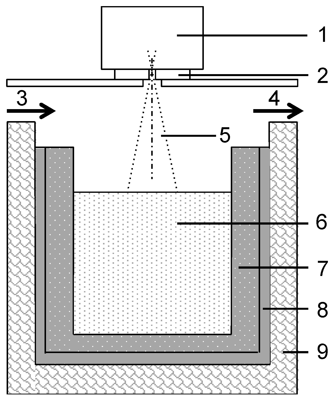
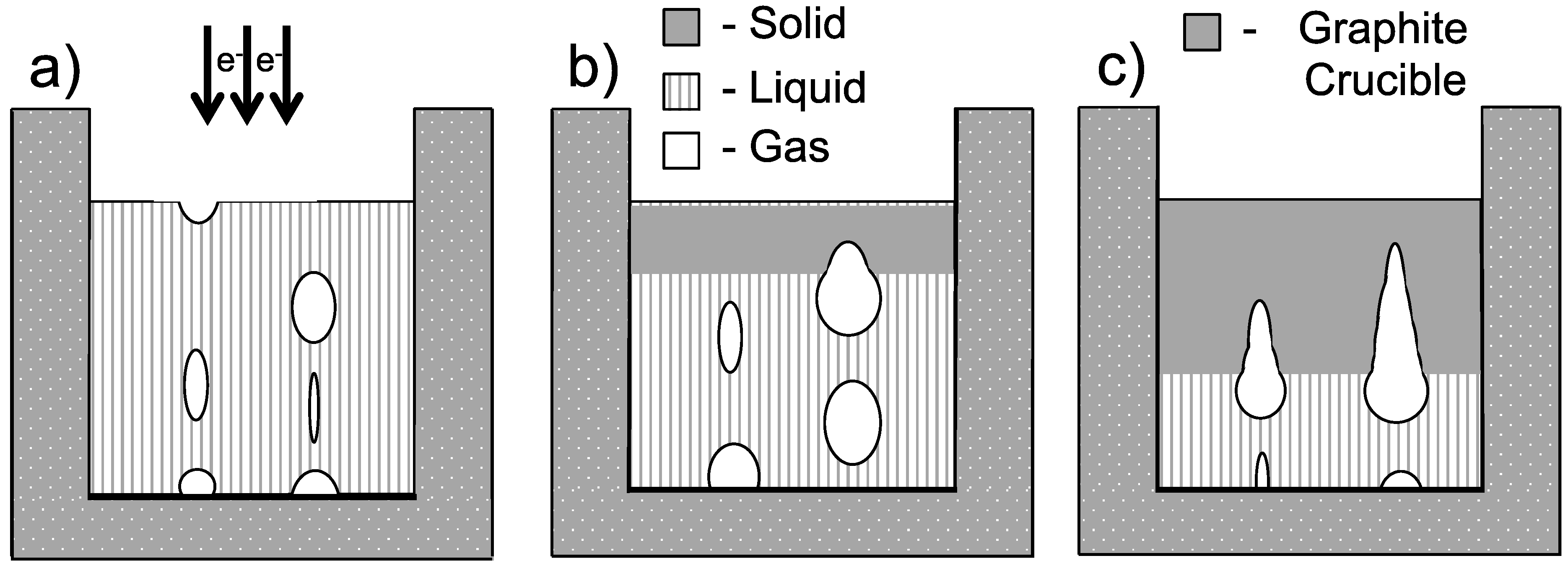
3.1. Originally Observed Channel Structures

For the original series of experiments, in general after about 30 min, the beam was switched off. As the aim of that original experimental series [5] was to produce nanopowders, attention was not paid to the target ingot. Thus multiple copper synthesis experiments were performed on the same ingot without it being removed from the crucible. Copper was occasionally added to the crucible to replenish the evaporated copper. After the experimental series, the graphite crucible with the copper was removed from the apparatus and kept in storage. It was only after 5 years, during which time different experiments were performed at the facility, that the graphite crucible was needed again and that the copper ingot was removed and the channel structures were first observed. The copper ingot weighed 3.3 kg and was 60 mm in height. Unfortunately, the exact conditions originally used are unknown and some minor modification have been made to the facility during that time. Figure 2a,b show a side view and a top view of the ingot. The ingot was a slightly conical shape with a top diameter of ~95 mm and a lower diameter of ~88 mm. There was an azimuthal ripple nonuniformity around the perimeter of the ingot with wavelength of about 15 mm and an amplitude of about 1 mm. Figure 2c,d show the channel structures found to form on the bottom of the ingot. The cavities were semi-regularly spaced with the channel structure diameters being about 5 mm. Furthermore, the channel structures seemed to be arranged as two concentric circles. The depth of the channels varied as indicated in Figure 2d. They had a conical shape; tapering from the bottom up. Although it is a common occurrence for some small holes to form in the process of casting a material, the regularity and depth of the channel structures was surprising and the main point of interest; prompting further investigations into their formation.
Figure 2. Original copper ingot with channel structures formed after copper nanoparticle synthesis experiments using electron beam evaporation. (a) Side view; (b) top view; (c) side-bottom view; and (d) bottom view with the channel structure depths labeled in mm.
Metals 05 00428 g002

3.2. Structures Observed with Varied Parameters

When the reactor was opened, for both gas configurations and copper grades, the copper ingot was observed to be solidified, although still hot with a bright orange-red color. After cooled to room temperature, the top surface and side surfaces of the samples were predominantly black in color due to oxidation of the hot copper surface (as in Figure 2a,b).
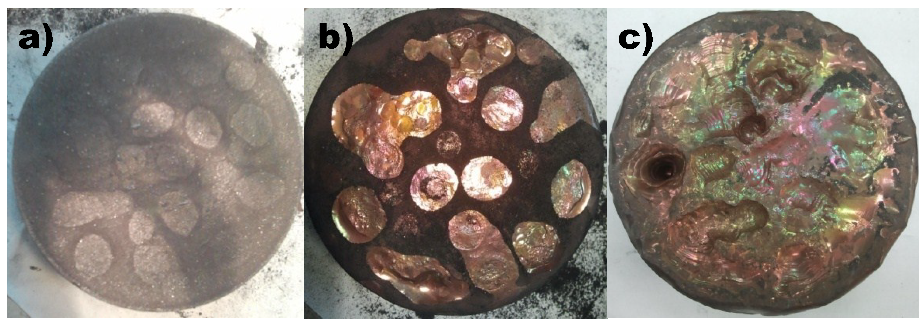
After experimental runs with the “open” gas flow configuration, the bottom surface of the ingots were mostly black in color (which may be due to contact with the graphite crucible or oxidation) with some copper-colored round spots. Hardly any indentation into the body of the ingot was observed (Figure 3a). The spot sizes approximately correspond with the size and shape of the channel structures formed in the ingot shown in Figure 2; thus appearing to be related to the vertical channel structures. On the sides of the ingot, some streaks of a slightly lighter black were observed to extend vertically—most noticeably from where the spots on the bottom of the ingot touched the edge of the bottom surface. Similar ingots were obtained from M0 and M1 copper. When a “closed” gas flow configuration was used, which can solidify the upper portion of the copper melt faster due to the higher achievable flow rates, for M0 copper (Figure 3b), a similar ingot to the ones obtained with the “open” gas flow configuration was obtained although a few very shallow indentations were present. For M1 copper in the “closed gas flow configuration (Figure 3c), some shallow channels formed with some occasional deeper channels although the distribution of channels was uneven.
Figure 3. (a) M1 copper ingot formed after electron beam evaporation experiments using an “open” gas flow configuration (low speed cooling); (b) M0 copper from a “closed” gas flow configuration (high speed cooling) and (c) M1 copper from the “closed” gas flow configuration.
Metals 05 00428 g003
Copper oxide in copper ingots can be identified through microscopic analysis by dark grey-blue specks inside copper [6,7]. These copper oxides can be distributed within the samples randomly as discreet specs (usually formed when the copper solid is formed through deformation) or be concentrated along the grain boundaries of copper as a Cu + Cu2O eutectic (Usually formed when the copper solid if formed through the crystallization of a melt) [6,8]. The microstructures of the M0 and M1 copper ingots were observed optically by cutting cross-sections from the samples and smoothing and polishing them. The microstructure of the as-received M1 and M0 samples before being exposed to the electron beam are shown in Figure S1. In these samples, the copper oxide specs are randomly distributed; with the concentration of specs being higher in M1 copper compared to M0 copper. 
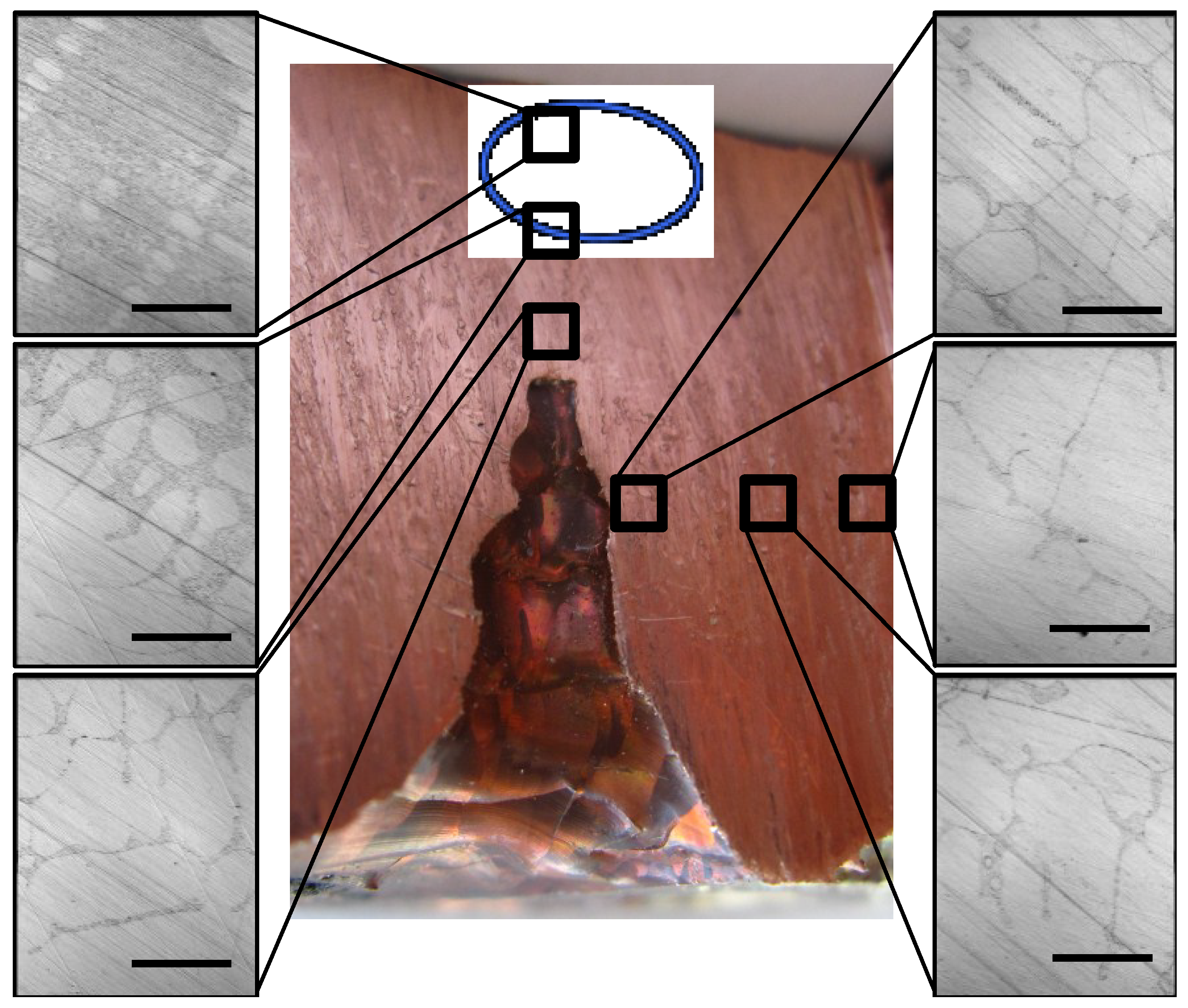
Figure 4 shows a cross-section on a M1 “closed” ingot through a large channel structure and the micrographs of various regions of the cross-section. A more detailed view of the microstructure distribution in the cross-section sample is shown in Figure S2 with panoramic micrograph scans across the sample. From the optical micrographs, it is observed that after the M1 sample is evaporated with the electron beam, the ingot recrystallizes with the copper oxides redistributed to the grain boundaries of the copper (seen as web-like structures) as a eutectic phase [6]. Metallographic analysis of this microstructure revealed an oxygen content of 0.06%; greater than the <0.01% oxygen content in the untreated M1 copper. An interesting area was found above the tip of the channel structure and near the top surface of the ingot (indicated with a blue circle in Figure 4). In this area, the copper oxide eutectic phase dominates over the copper phase and has an oxygen concentration of 0.15%. The region is about 8.5 mm above the tip of the channel structure, is biased more towards the central region of the ingot (where the electron beam would hit), and is about 6 mm in width and 2.5 mm in height. This type of region was observed over other holes as well. Another example can be seen above a shallower channel structure in Figures S3 and S4. Over this channel structure, the region of high copper oxide concentration was about 10.5 mm above the tip of the channel structure, also biased towards the central region of the ingot, and 6 mm in width and 1 mm in height. Thus, it seems these hypereutectic regions are linked to the location and depth of the channel structures as well as to the location of the area directly heated by the electron beam. It was also observed that next to the crucible-copper interface and upper surface of the copper, a large concentration of non-metallic inclusions were present. Near the base of the channel structures and from the tip towards the hypereutectic region, some non-metallic inclusions were observed.
Figure 4. Photograph of a cross section of a channel in a M1 copper ingot from the “closed” gas flow configuration. The top of the image is where the ingot would be exposed to the electron beam and copper vapors would evolve from during the copper nanoparticle synthesis experiments. The bottom of the image shows the bottom of the copper ingot which would be touching the graphite crucible during the copper nanoparticle synthesis experiment. The right-hand side approaches the central region of the ingot while the left-hand side approaches the outer edge of the ingot. Optical microscopy images (100×, scale bars = 425 µm) obtained from various regions of the sample are shown in the insets and reveal the copper oxide distribution within the sample. The blue circled region represents the approximate location of the high concentration of copper oxides.
Metals 05 00428 g004
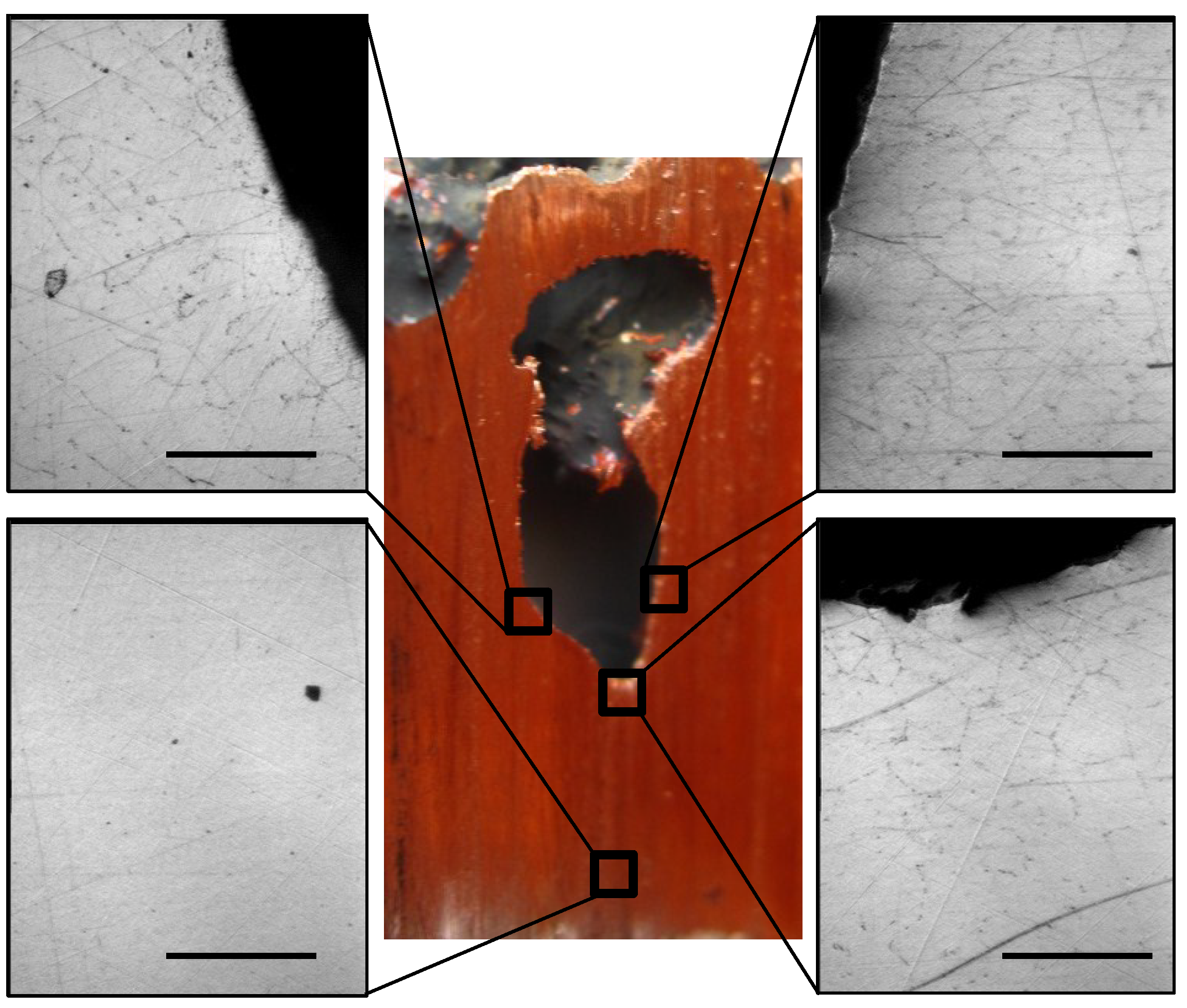
When a M0 “closed” samples was cut near the central region, a void was found near the upper surface of the ingot (Figure 5). While for the most part, the void was contained inside the ingot, there was a small hole connecting it to the outside atmosphere—also demonstrated by the black color of the surface of the void. The microstructure of the M0 copper after being evaporated with an electron beam appeared unchanged from the microstructure of the as-received M0 copper; although the oxygen concentration increased to 0.03% from <0.01%. However, around the void, the web-like concentration of copper oxides on the grain boundaries of copper was observed which extended for about a mm from the surface of the void (more detail of the microstructure distribution around the void can be seen in Figure S5). These areas had the same oxygen content of 0.06% as the web-like regions in the M1 copper from the “closed” configuration.
Figure 5. Photograph of a cross section of a M0 copper ingot from the “closed” gas flow configuration in which a void was found near the center of the upper surface of the ingot. The top of the image is the top surface of the sample. Optical microscopy images (100×, scale bars = 425 µm) obtained from various regions of the sample are shown in the insets and reveal the copper oxide distribution within the sample.
Metals 05 00428 g005
Additional experiments were conducted using different conditions. One experiment was conducted by filling shavings of M1 copper into a crucible then irradiating for 5 min at 5 mA then 5 min at 7 mA in the “open” gas configuration. The obtained ingot is shown in Figure S6. In Figure S6a, the area of the ingot which was hit by the electron beam can clearly be seen; the melted copper solidified as a thin block on the bottom of the crucible. The bottom surface of the block (Figure S6b) contained small indents near the center of the block. Thus it seems that even in thin layers of copper, the channel structures can form. A graphite lid was then placed on the graphite crucible which covered areas not hit by the electron beam. The ingot in Figure S6 was irradiated further for 20 min at 7 mA. The resulting ingot possessed wider shallow channels on the bottom as well as some indents on the side surface of the ingot (Figure S7). The indents on the side surfaces had a slight curvature towards the upper surface of the ingot.

4. Discussion

Konovalov et al. [7,9] investigated how the interaction of molten copper with graphite crucibles caused the apparent boiling of the copper at around 1200 °C, much below its 2562 °C boiling point. The boiling of the copper is thought to occur from the interaction of the carbon with oxygen in the copper to form carbon oxide gasses [7,9,10]. Thus, as channel structures were only observed to originate at the interface between the molten copper and graphite crucible, evolved carbon oxide gasses are thought to be responsible for the formation of the channel structures. As molten copper will only wet graphite where it is rough, due to burning out of some of the graphite, it is possible that the carbon oxides only evolved from certain spots on the graphite crucible. As molten metals heated by an electron beam are known to have a high Rayleigh number [11], convection currents would be expected to be present in this system. Thus, the location of the channel structures may be determined by defects in the graphite crucible used and convection currents present in the copper melt.
Between the copper ingot samples created using the “open” and “closed” gas flow configurations, only those from the “closed” configuration created any channel structures; the “open” configuration only forming spots on the bottom surface of the ingots. Between the gas configurations, the main difference is the cooling rates of the top surface of the copper—“open” being higher. Although a water-cooling system exists in the experiment, its main use is to cool the steel enclosure of the crucible so that it does not melt. As the graphite crucible is insulated from the steel wall by graphite powder, the main cooling source of the copper melt is considered the argon gas flow. Comparing the M1 and M0 copper ingots in the “closed” gas flow configuration, M0 had almost no channel structures, only spots on the bottom of the ingot. The main difference between these two copper grades is their oxygen content. Thus it is expected that the carbon oxide gas evolution rate in M0 copper would be less than in M1. Thus, a mechanism of formation for the channel structures is proposed based on the solidification of the copper melt trapping evolved gas bubbles. For systems in which the cooling rate is fast enough, solidification of the top surface of the copper melt would prevent gas bubbles from escaping the copper. As the solidification front moves down, gas bubbles trapped against the solid are frozen as vacancies. Subsequent gasses which rise into the vacancy expand the bubble in the underlying liquid. Thus, the channel structure is expected to grow from the top down along with the solidification front of the copper. In the end, the gas bubbles may escape from the bottom to the sides of the ingot, causing the streak patterns observed on the sides of the ingots. This process is illustrated in Figure 6. In the “open” configuration with its slower cooling rate, it is thought that the gas bubbles all escape from the top of the molten copper before it solidifies; leaving only spots on the bottom of the ingot. However channels could still be created for thin samples as shown in Figure S6 as the high surface area to volume ratio of the sample could have allowed for rapid cooling. For the M0 copper in the “closed” configuration, the rate at which gas bubbles evolved may have been too slow to form channels before solidification took place and bubble production stopped. The vacancy observed in Figure 5 appears to be a gas bubble vacancy frozen into the copper just as the gas bubble was escaping. This demonstrates that some bubbles did form in the M0 system (as do the spots on the bottom) and supports the proposed mechanism of formation for the channel structures. The gas bubble can only evolve if the pressure of the gas is greater than the sum of the atmospheric, hydrostatic, and Laplace pressures [7]. The experiments performed with a cover on the crucible (Figure S7) would have had an increased atmospheric pressure which may have hindered the gasses from evolving. However the increased pressure may also increase wetting of the crucible with copper. Thus in this case, the formed bubbles may have remained trapped at the lower surface of the crucible until the copper solidified.
Figure 6. Schematic of the formation of the channel structures in a cooling copper melt. (a) While the electron beam is still irradiating the copper, gas bubbles rise through the molten copper; (b) After the electron beam is turned off, the top of the copper begins to solidify; trapping a void from a gas bubble; (c) The copper is further solidified, the channel structures growing in the solid.
Metals 05 00428 g006
The hypereutectic region formed above the channel structures (as seen in the micrographs of the M1 from the “closed” gas configuration) are also of interest but their origin is still unclear. The bias of the location of the regions towards the center of the ingot (where the copper melt is hottest due to the electron beam hitting it directly) suggests a relation to the densities of copper and copper oxide (ρ(Cu) = 8.96 g cm−3, ρ(Cu2O) = 6.0 g cm−3 at room temperature and ρ(Cu) = 7.784 g cm−3 at 1217 °C [12]) with the less dense Cu2O moving towards the less dense zone of copper as well as to where it is more soluble. As in all observed locations, the hypereutectic region was present about a centimeter above the tip of a channel structure, a relation to the gas evolution is suggested. As the “closed” gas configuration had the possibility to introduce some oxygen into the system, it may be possible that the increased partial pressure of oxygen from the gas bubbles promoted the formation of these hypereutectic regions and factors such as density, solubility, and convection currents raised the hypereutectic regions above the gas bubbles to where they were subsequently solidified. Slight increases in the oxygen content directly around the bubbles may not have been observed around the M1 channels due to the overall higher inherent oxygen content but were noticeable in the bubble trapped in the M0 copper (Figure 5 and Figure S5) with the change in microstructure. Another possibility is the carbon oxides dissolving into the copper from the gas bubbles and subsequently decomposing; leaving oxygen that forms into copper oxides and carbon that remains in the copper as a non-metallic inclusion. This is supported by the observed non-metallic inclusions although carbon is known to have a low solubility in copper [13].
The results of these experiments serve as a warning to the use of copper ingots after they have been used in electron beam evaporation. The oxygen content is increased and the distribution of copper oxides can be significantly changed. Researchers must be aware of the changes in the copper for subsequent experiments. The experiments have revealed that the highest oxygen content regions are found above the areas of gas evolution. Slower cooling rates of the samples after electron beam irradiation can help lower the amount of additional oxygen incorporated into the copper and hinder or prevent the formation of channel structures.

5. Conclusions

Vertical channel structures were observed from the bottom up in copper ingots after using them to synthesize copper nanoparticles using electron beam evaporation techniques. Various conditions such as gas flow configuration and oxygen content in the starting copper were varied in order to investigate the formation of these channel structures. The channel structures were likely formed due to gaseous carbon oxide bubbles formed between the interface of the graphite crucible used and oxygen in the molten copper along with the cooling rate of the copper melt. After the electron beam was shut off, the copper melt was cooled from the top down, preventing the gas bubbles from escaping and eventually solidifying the vacancies left by the bubbles in the melt to form channel structures. Additionally, the microstructures found in the resultant ingots were of interest, as hypereutectic regions were found above the channel structures while absent in other areas. These likely formed due to changes in the partial pressure of oxygen where the gas bubbles formed as well as carbon oxides decomposing in the melt.

Acknowledgments

The authors are grateful to colleagues who took part in the experiments, and the discussion of possible causes of the phenomenon and analyzes: P.S. Prozorenko, I.K. Chakin, M.G. Golkovski, S.S. Garmaev, V.A. Ushakov, N.A. Romanov, B.B. Baldanov. The Revda Non-ferrous Metals Processing Works is acknowledged for providing oxygen content measurements of the samples.
The study was performed as part of the Ministry of Education and Science of the Russian Federation contract №16.1930.2014/K.

Author Contributions

S.B. came up with the main idea of the experiment; A.N., R.S., K.Z., A.Z., and E.K. prepared and conducted the experiments; S.B., A.N., A.R., and M.S. analyzed the data; S.B. and M.S. wrote the manuscript.

Conflicts of Interest

The authors declare no conflict of interest.

References

  1. Lukashov, V.P.; Bardakhanov, S.P.; Salimov, R.A.; Korchagin, A.I.; Fadeev, S.N.; Lavrukhin, A.V. A method of producing of fine silicon dioxide, installation of its implementation and fine silicon dioxide. Patent RU №2067077, 27 September 1996. [Google Scholar]
  2. Bardakhanov, S.P.; Korchagin, A.I.; Kuksanov, N.K.; Lavrukhin, A.V.; Salimov, R.A.; Fadeev, S.N.; Cherepkov, V.V. Nanopowders obtained by evaporating initial substances in an electron accelerator at atmospheric pressure. Dokl. Phys. 2006, 51, 353–356. [Google Scholar] [CrossRef]
  3. Bardakhanov, S.P.; Korchagin, A.I.; Kuksanov, N.K.; Lavrukhin, A.V.; Salimov, R.A.; Fadeev, S.N.; Cherepkov, V.V. Nanopowder production based on technology of solid raw substances evaporation by electron beam accelerator. Mat. Sci. Eng. B 2006, 132, 204–208. [Google Scholar] [CrossRef]
  4. Kuksanov, N.K.; Korabelnikov, B.M.; Kosilov, M.R.; Nemytov, P.I.; Prudnikov, V.V.; Salimov, R.A.; Veis, M.E. Development of the next generation of powerful electron accelerators. Radiat. Phys. Chem. 1995, 46, 481–484. [Google Scholar] [CrossRef]
  5. Zavjalov, A.P.; Zobov, K.V.; Chakin, I.K.; Syzrantsev, V.V.; Bardakhanov, S.P. Synthesis of copper nanopowders using electron-beam evaporation at atmospheric pressure of inert gas. Nanotech. Russ. 2014, 9, 660–666. [Google Scholar] [CrossRef]
  6. Copper: Methods of determination of oxygen. Russian Standard 13939.13–93. (In Russian)
  7. Konovalov, A.N. Investigation of melting and deoxidation copper to obtain alloy electrodes from chromium bronze. Ph.D. Thesis, Moscow Institute of Steel and Alloys, Moscow, Russia, 16 May 2011. [Google Scholar]
  8. Neuman, J.P.; Zhong, T.; Chang, Y.A. The Cu-O (Copper-Oxygen) system. Bull. Alloy Phase Diagr. 1984, 5, 136–140. [Google Scholar] [CrossRef]
  9. Konovalov, A.N.; Pikunov, M.V.; Gerasimov, S.P. “Boiling” the melt during copper remelting. Russ. J. Non-Ferr. Met. 2009, 50, 218–220. [Google Scholar] [CrossRef]
  10. Ten, E.B.; Badmazhapova, I.B.; Kimanov, B.M. Kinetics of the Carbon reduction of liquid copper. Steel Trans. 2008, 38, 533–536. [Google Scholar] [CrossRef]
  11. Karcher, C.; Kolesnikov, Y.; Andreev, O.; Thess, A. Natural convection in a liquid metal heated from above and influenced by a magnetic field. Eur. J. Mech. B 2002, 21, 75–90. [Google Scholar] [CrossRef]
  12. Brillo, J.; Ergy, I. Density determination of liquid copper, nickel, and their alloys. Int. J. Thermophys. 2003, 24, 1155–1170. [Google Scholar] [CrossRef]
  13. Oden, L.L.; Gokcen, N.A. Cu-C and Al-Cu-C phase diagrams and thermodynamic properties of C in the alloys from 1550 °C to 2300 °C. Metal. Trans. B 1992, 23, 453–458. [Google Scholar]

