

Microstructural Investigation of a FeMnAlNi Shape Memory Alloy Processed by Tungsten Inert Gas Wire and Arc Additive Manufacturing

Institut für Werkstoffkunde (Materials Science), Leibniz Universität Hannover, 30823 Garbsen, Germany
*
Author to whom correspondence should be addressed.
Metals 2022, 12(10), 1731; https://doi.org/10.3390/met12101731
Submission received: 14 September 2022
/
Revised: 6 October 2022
/
Accepted: 12 October 2022
/
Published: 16 October 2022
(This article belongs to the Special Issue Additive Manufacturing of Metallic Materials: Characterization, Properties, and Modeling)
Abstract
:In the present study, tungsten inert gas wire and arc additive manufacturing was used to process an iron-based FeMnAlNi shape memory alloy. By a layer-by-layer method, a wall structure with a length of 60 mm and a height of 40 mm was generated. Bidirectional welding ensured grain growth parallel to the building direction. To maintain a nearly constant temperature–time path upon cooling, the structure was fully cooled after each weld to room temperature (298 K). With this approach, an anisotropic microstructure with a grain length of up to 8 mm (major axis) could be established. The grain morphology and formed phases were investigated by optical microscopy and scanning electron microscopy. The images revealed a difference in the orientation with respect to the building direction of the primarily formed γ grains along the grain boundaries and the secondarily formed γ grains in the heat-affected zones. Subgrains in the α matrix were observed also by scanning electron microscopy. With X-ray diffraction, the preferred orientation of the α grains with respect to the building direction was found to be near ⟨100⟩. Overall, an anisotropic polycrystalline material with a columnar texture could be produced, with a preferred grain orientation promising high values of transformation strains.
1. Introduction
Shape memory alloys (SMAs) feature special mechanical properties. NiTi alloys, which were discovered by Buehler et al. [1] are still the most widely used SMA. NiTi-based systems and all ternary and quaternary compounds are characterized by high pseudoelasticity (pseudoelastic transformation strains up to 10% in a single crystalline material) [2,3,4], a high temperature dependence of the critical transformation stress dσc/dT of between 5 and 8 MPa K−1 [5,6,7] and high production costs combined with poor cold workability [8]. Fe SMAs, such as FeMnSi [9,10], FeNiCoAlTa [11] and FeMnAlNi [12], provide a lower-cost alternative to the NiTi-based systems while exhibiting promising processing properties. Omori et al. demonstrated pseudoelastic transformation strains of up to 5% for Fe43.5Mn34Al15Ni7.5 [12]. A particular advantage of this novel iron-based SMA is the low temperature dependence of the critical transformation stress dσc/dT of only 0.53 MPa K−1 [12]. The combination of low-cost materials and low temperature dependence makes Fe-based SMAs particularly interesting for civil engineering, especially in damping applications.
Conventional iron-based alloys usually undergo a phase transition from a γ phase (A1, fcc) to an α phase (A2, bcc), where an altered α/γ equilibrium can be observed at high Mn-X contents (X: ferrite-stabilizing element). With increasing Mn-X content, a characteristic γ loop, similar to the binary FeCr system, forms [13]. The equilibrium temperature , defined by the equality of the Gibbs energy of the α phase as well as the γ phase, can be calculated for different Mn-Al contents of the FeMnAl alloy by the CALPHAD (calculation of phase diagrams) method [12,13]. The α phase is stabilized at the Curie temperature up to 30 at.% Mn, resulting in the formation of a γ loop in the phase diagram, and a conventional γ/α′ martensitic transformation (MT) takes place. At >30 at.% Mn and >15 at.% Al, the decreases to near room temperature, which stabilizes the γ phase at room temperature, resulting in an α/γ′ MT [12]. The altered phase transition is caused by the magnetic contribution to the Gibbs energy, as the Gibbs energy can be separated into a magnetic and a non-magnetic contribution. With increasing Mn and Al content, the magnetic contribution to the Gibbs energy decreases, lowering the , and the γ phase is stabilized at low temperatures [12].
The rapid functional degradation of polycrystalline SMA is partly caused by grain misorientations due to the anisotropic nature of σc, as well as grain boundaries and especially grain boundary triple junctions, leading to the activation of unfavorably interacting martensite variants [14,15,16,17,18]. Overall, the magnitude of the shape memory effect (SME) is determined by the grain morphology and grain orientation. On the one hand, the SME can be improved by controlled precipitation of the γ phase along the grain boundaries [19], and on the other, by reducing the total grain boundary interface. In the case of Fe-based SMA, the grain morphology and in particular the grain size can be altered by exploiting the abnormal grain growth. This minimizes the overall grain boundary interface, and the ratio of the grain diameter to specimen thickness typically becomes greater than one [20,21]. The so-achieved oligocrystalline microstructure enables a pseudoelastic reversibility of Fe43.5Mn34Al15Ni7.5 up to 5%, which is already observable at room temperature [12,21]. Depending on the loading direction, different martensite variants are available to accommodate the load [22,23,24]. Using the energy minimization theory [25] for the twinned martensite and the lattice deformation theory [26] for the detwinned state of the martensite, different theoretical transformation strains are obtained depending on the crystallographic direction. For both twinned and detwinned states, the near 〈100〉 direction shows maximum transformation strain. In contrast, the 〈111〉 direction is less favorable. Experimentally, however, the highest transformation strain was found along 〈123〉 [23,24].
In contrast to conventional manufacturing processes, such as casting and forming, the components can be manufactured with additive manufacturing (AM) to a near-net shape in a layer-by-layer fashion with high geometric complexity [27,28]. However, increased set-up times, as well as the preparation of the initial material, might increase the overall process costs [29,30]. As shown in [31] and according to ASTM 529000AM, AM can be divided into seven main groups. However, only directed energy deposition (DED) and powder-bed fusion (PBF) are widely used. Wire and arc additive manufacturing (WAAM) processes are assigned to the DED group, which also includes the arc processes such as metal inert gas (MIG), tungsten inert gas (TIG) and plasma welding. In contrast to the MIG process, there is no short circuit transition of the molten material in the TIG process. Therefore, arc stability and heat input are constant, and a spatter-free material transfer can be ensured [32,33]. Additionally, the microstructure can be tailored by varying the process parameters during AM, allowing control of the mechanical properties throughout the manufacturing process [31,34,35].
Various studies on AM showed that a 〈100〉 columnar texture is formed in cubic primary solidifying alloys [31,36,37,38]. The 〈100〉 direction is an easy growth direction for bcc and fcc solidifying phases when anisotropic conditions apply, as is the case during AM [39,40,41]. The formation of strong textures is influenced by the temperature gradient grad T and the solidification rate R. The large temperature gradient between the melt pool and the base material favors an epitaxial growth of the crystals in the melt from the partially molten grains of the base material. For the heterogeneous nucleation that occurs in this way, a significantly lower activation energy ΔGA is necessary. Consequently, a lower supercooling ΔT is needed for nucleation [42]. The solidification front is directed against the heat flux, and grains grow beyond the individual layers [31]. The dependence of grain growth on grad T and R during the AM of FeMnAlNi has already been investigated in several studies. As shown for the selective laser melting of FeMnAlNi, the grain morphology is impacted by the geometry in the case of fixed processing parameters [37]. While for small dimensions (specimen diameter ≈ 0.5 mm) a 〈100〉 columnar grain growth occurs, this texture disappears with increasing dimensions (specimen diameter ≈ 5 mm). The change of the geometrical shape leads to a different solidification mode and therefore to a change of texture. In [36] it is shown that a variation of the cooling conditions during the laser powder-bed fusion process leads to a different correlation between the formed grain morphology and the specimen dimensions. An elevated building platform temperature causes a microstructure transition of equiaxed grains with irregular orientation to a 〈100〉 columnar texture with increasing specimen diameter, while in [37] the opposite was reported. Still, both studies showed an epitaxial growth of the grains past the individual layers with a mean grain length of about 0.5 mm.
With the aim to achieve a pronounced columnar texture with an overall low grain boundary interface in the polycrystalline FeMnAlNi, AM with a high deposition rate, in particular the TIG WAAM process, was used in the present study. WAAM components made from FeMnAlNi are attractive for damping applications, and the columnar texture is favorable as it minimizes the intergranular strain. The higher deposition rate compared to PBF processes should result in grains with a larger major axis than those obtained from low deposition rate processes promising less susceptibility to cracking upon cyclic loading. In the present study, bidirectional welding was used to maintain the preferred growth direction parallel to the building direction. Grains and phases formed were investigated using optical microscopy (OM) and scanning electron microscopy (SEM). In addition, the heat-affected zone (HAZ) between individual layers, as well as the γ phase, was examined closely by SEM. The texture was investigated using X-ray diffraction (XRD). Lastly, thermomagnetization was measured, and the ramifications of the data with respect to the application in mind are discussed.
2. Experimental Section
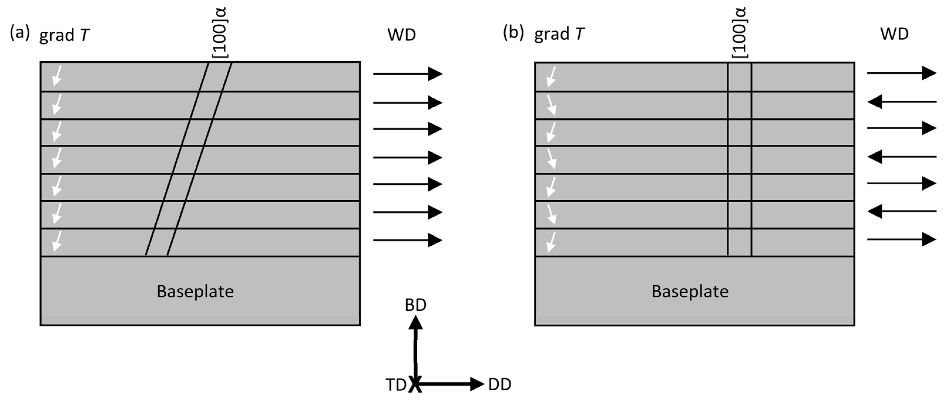
Cast and hot-rolled FeMn34Al15Ni7.5 (nominal composition) was industrially processed by thyssenkrupp Steel Europe AG (Duisburg, Germany). A 64 mm × 45 mm × 6 mm plate was cut from an ingot of the material and placed on a copper plate, which was cooled by internal water cooling to approx. 289 K. The filler material used as the initial material was machined from a hot-rolled 2 mm FeMn34Al15Ni7.5 plate by abrasive water-jet cutting. The resulting stripes with a cross section of 2 mm × 2 mm were placed and fixed on the base plate for the first weld layer. Later, the filler material was placed on the already welded layers to generate a wall structure with a width of 7 mm. The feed of the filler material therefore equaled the welding speed. The TIG torch (Abicor Binzel, Busek, Germany) was mounted on a MOTOMAN HP20 robot (Yaskawa Europe, Eschborn, Germany), ensuring a constant torch angle of 90° and a constant welding speed of v = 5 mm s−1. An EWM TETRIX 521 AC/DC COMFORT FWD (EWM, Mündersbach, Germany) served as the source. Each weld was performed in direct current mode with 120 A and a shielding gas composition of 70/30 Ar/He (Ar: ARCALTM Prime (99,998%), He: Lasal 4 (99,996%); Air Liquide S.A., Paris, France) with a volume flow of 12 L s−1. A total of 17–22 welds were used for each additively manufactured structure, yielding structures with dimensions of about 40 mm × 7 mm × 18.5 mm. As shown in [43], the growth direction of 〈100〉 is affected by the welding direction during AM using a DED process. For a unidirectional welding process, the 〈100〉 is tilted in the welding direction (WD), whereas the heat flux is directed against the WD (Figure 1a). In order to obtain a grain growth parallel to the building direction (BD) during the processing, bidirectional welding was employed in the present study. The resulting alternating temperature gradient in each layer leads to a mean temperature gradient perpendicular to the base plate and parallel to the BD, and therefore the 〈100〉 direction is also parallel to the BD (Figure 1b). After each weld, the structure was first cooled to room temperature in air, still placed on the cooled copper plate. In this way, a sufficient cooling rate between each weld and a suppression of the α→γ transformation was intended.
Cross-sections with a thickness of 6 mm were used for microscopic examination and XRD analysis. One cross-section was prepared in the BD–TD plane (cf. Figure 1b) for the coordinate system), a second in the DD–TD plane and a third in the BD–DD plane. First, the specimens were ground and then polished (0.06 µm, VIBROMET 2: Buehler, Echterdingen, Germany). After polishing, XRD measurements were carried out on a BRUKER D8 (Bruker Corperation, Billerica, MA, USA) equipped with a two-dimensional detector using Co-Kα radiation. The texture measurements were taken ranging from 34.5 to 69.6 °2Θ, 58.9 to 93 °2Θ and 80.7 to 114.8 °2Θ, as well as φ-angles of 16°, 35.5° and 55° with a ψ-rotation of 360°. With this approach, the {110}, {200} and {211} could be considered for the calculation of the orientation density function (ODF) and the recalculation of the pole figures. Samples were then etched with a solution of 2% HNO3 (ROTH, 68%, pure) and ethanol (CVH, 99%). OM was performed on a ZEISS OLYMPUS BX53M (Carl Zeiss AG, Oberkochen, Germany). A VISITEC MIRA XV SEM (VisiTec Microtechnik, Grevesmühlen, Germany), equipped with a backscattered electron (BSE) detector (ELLCIE, Grevesmühlen, Germany) and a detector for energy dispersive X-ray spectroscopy (EDS) (Thermo Fisher Scientific, Waltham, MA, USA), was used at an accelerating voltage of 20 keV, a beam current of 70–150 pA for microstructural analysis and a beam current of up to 450 pA for EDS analysis. Inductively coupled plasma-optical emission spectroscopy (ICP-OES, SPECTRO CIROS VISION EOP) (SPECTRO Analytical Instruments, Kleve, Germany) was employed to determine the chemical composition of the initial filler material and the as-built structure. For this purpose, three specimens were cut from the same 2 mm × 2 mm filler material stripe, while the specimens for the as-built state were sectioned from the center of a smaller 2.5 mm-thick cross section. For thermomagnetization tests, a specimen with a length of 12 mm in BD and a cross section of 2.5 mm × 2.5 mm was cut using electrical discharge machining. Thermomagnetization was recorded in the temperature range of 125 to 450 K in an external magnetic field with a flux density of 27.55 µT. For this purpose, the response of the sensor coil resulting from the change in the electric susceptibility of the specimen with temperature was measured.
3. Results and Discussion
3.1. Chemical Composition
The mean chemical composition of the filler material and the as-built state are shown in Table 1. The filler material differs only by 1.7 at.% in the Mn content and by 1 at.% in the Al content, indicating a close to nominal composition obtained with the industrial process route. As seen by the low Mn content of the as-built state, which differs by 5.3 at.% from the nominal and literature composition, a loss of alloying elements took place during AM. The Mn content significantly influences the phase regions in the phase diagram and the magnetic properties, so the effect of the Mn loss was evaluated further. The loss of the Mn during the process can be attributed to the high affinity of the manganese to react with any remaining oxygen, forming manganese oxide.
3.2. Microscopy
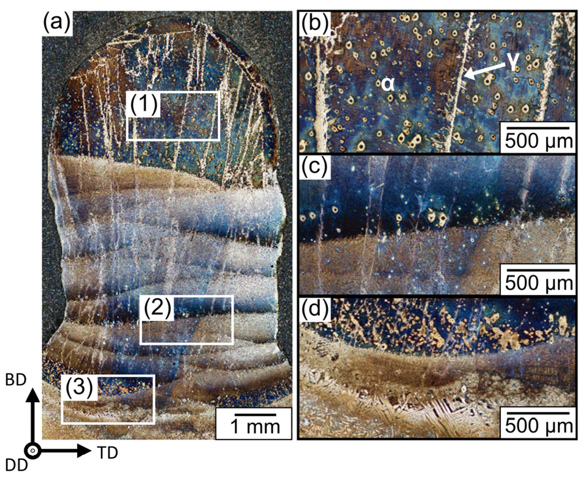
Figure 2 shows optical microscopy images of the BD-TD section. As seen in Figure 2a, grain growth is nearly parallel to the BD. The temperature conditions lead to heterogeneous solidification being preferred over homogenous solidification. Further, a strong solidification texture of the α grains is present across the individual layers, so epitaxial solidification controlled by high grad T/R ratio can be assumed. Whether this texture actually exhibits the 〈100〉 preferred orientation typical of bcc solidifying phases was clarified by XRD. Nevertheless, it is already apparent that AM with TIG-WAAM achieves a pronounced columnar grained microstructure, even when large sample cross-sections are considered. At the same time, grains with a major axis of up to 5.5 mm are present in BD, which are an order of magnitude longer than for structures produced with a low deposition rate, such as PBF processes [36,37]. The enhanced grain growth reduces the grain boundary surfaces, lowering susceptibility to functional fatigue during loading tests. In Figure 2b, the area of the last welded top layer is shown enlarged. The γ phase has precipitated mainly along boundaries of the α grains. For the mechanical properties, the precipitated γ phase is beneficial as it suppresses intergranular cracking [19]. Although cooling between the individual layers to approx. 298 K was maintained to minimize α→γ phase transformation, Figure 2c shows that a large area with a γ phase occurs between the weld layers, forming a heat-affected zone (HAZ). Due to the layer-by-layer processing, the majority of the area of the prior welded layer is molten by welding a new layer on top. Therefore, only a small part of the previously α-bcc solidified structure remains, and a new HAZ forms between the old and new seam. An almost-complete α→γ phase transformation takes place. Despite the phase transformation, the orientation of the remaining α matrix is preserved so that epitaxial growth causes the grains to grow over several layers. The high γ content influences the SME as the γ-fcc phase does not participate in the α-bcc→γ′-fcc MT and actually suppresses the MT due to the higher ductility. As described above, a major proportion of the arc’s power was used to melt the previously welded layer. By increasing the wire feed rate, the proportion of the molten, previously welded layer could be reduced, and simultaneously most of the energy would be used to melt the filler material instead. With this approach, the overall proportion of the γ phase in the specimen could be controlled. Figure 2d shows a magnification of the first layer. The HAZ of the first layer, which formed between the base material and the weld zone, is less pronounced than the HAZ in later welded layers. Since the base plate was placed directly on the cooled copper plate, the highest temperature gradient appeared during the weld of the first layer. Thus, a major part of the heat is dissipated via direct conduction. This may have led to a rapid passage of the α→γ phase transformation region and therefore to a narrow HAZ. With the increasing height of the wall structure, the heat will be less dissipated via convection since the temperature gradient decreases with increasing distance to the cooled copper plate, leading to heat accumulation and therefore to a broader HAZ. With each new welding layer, the previous solidification structure is first molten, then it solidifies with epitaxial growth and a grain selection takes place, and thus a preferential growth of grains that are favorably oriented with respect to the heat flux occurs. The α grains of the first layers are not as prominent as in the welding layers applied later, since unfavorably oriented grains will overgrow, and the overall content of preferential orientated grains increases with the wall built up.
To verify the assumptions made based on Figure 1 regarding the influence of uni- and bidirectional welding on grain growth, the BD-DD cross-section was analyzed. In Figure 3a, an overview of the BD-DD section is shown, while in Figure 3b some of the larger grains are highlighted in red, which have grown beyond several welding layers and HAZ (white lines in Figure 3b). The major axis of these intense grown grains reaches up to 8 mm. As mentioned, the bidirectional welding should ensure a grain growth parallel to the BD. When the major axis of the highlighted grains in Figure 3b are considered, it becomes apparent that the major axis deviates only slightly from being parallel to BD.
Figure 4 shows the OM images taken from the DD-TD section at the level of the top layer. In the overview (Figure 4a), areas with grains possessing a small diameter (Figure 4b) of approx. 65–180 µm (major axis) and areas with grains with a large diameter (Figure 4c) of up to 1.2 mm (major axis) can be identified. While grains with small diameters tend to occur at the edges, the grains with a larger diameter are located in the center of the specimen. This is congruent with the grain structures in Figure 2a, since in the BD-TD section the grains with the largest diameter are also located in the center of the specimen. During the solidification process, it is likely that frequent grain formation occurs at the interface between the melt pool and surrounding air. The grains formed at the interface can also be seen in Figure 2a at the upper end of the last welded layer. Due to a lower grad T/R ratio and the fact that the formation of new grains at the interface competes with epitaxial growth, the grains at the interface are not as pronounced as those in the center of the specimen. In addition, the grains at the interface will melt and re-solidify during the next weld. Besides the grain morphology, the γ phase precipitated along the grain boundaries and does not occur in clusters in the interior of the grain.
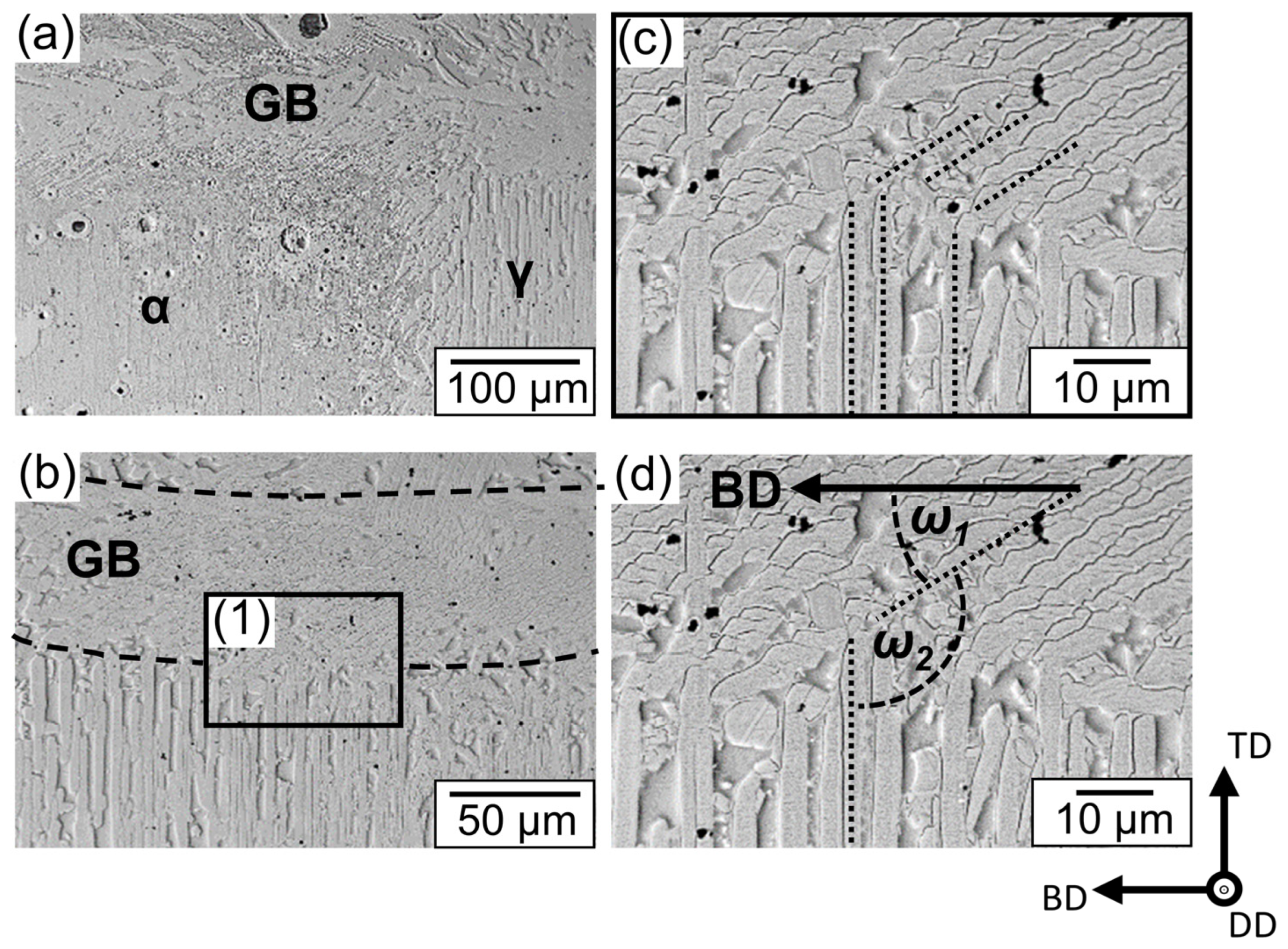
In Figure 5, the transition of an α grain of the top layer to the HAZ and the transformed α + γ two-phase region of the BD-TD section are shown. As seen in the SEM overview of the region (Figure 5a), the grain boundary can still be identified in the transformed region. At a higher magnification (Figure 5b), a globular-to-lamellar structure of the γ phase along the grain boundary is recognizable. The γ phase has grown, starting from the grain boundary, inside the α grain. In addition to the γ phase at the grain boundary, a pronounced lamellar structure of γ grains in the α matrix is present in the transformed region of the HAZ. When the transition from the primarily formed γ grains at the grain boundary to the secondarily formed γ grains in the grain interior is considered (Figure 5c), an angular relationship between the two grain structures and regarding the BD becomes apparent (indicated by the dashed lines in Figure 5d). The angle between the primarily formed γ grains and the BD is ω1 = 30–36° and the angle between the primarily and secondarily formed γ grains is ω2 = 120–136°. It is assumed that a change in the temperature–time course and a change in the direction of the heat flux and temperature gradient during the transformation of the primarily and secondarily γ grains have led to different preferred growth directions. Thus, the grain boundary is still visible even after the α→γ phase transformation in the grain interior. In addition to phase transformation in the grain interior, further α→γ phase transformation took place during the weld of a new layer in the area of the grain boundary. As a result, the α phase remaining after the primarily γ grain formation also transforms, and thus the density of γ grains increases and only a small proportion of α matrix remains in the grain boundary area.
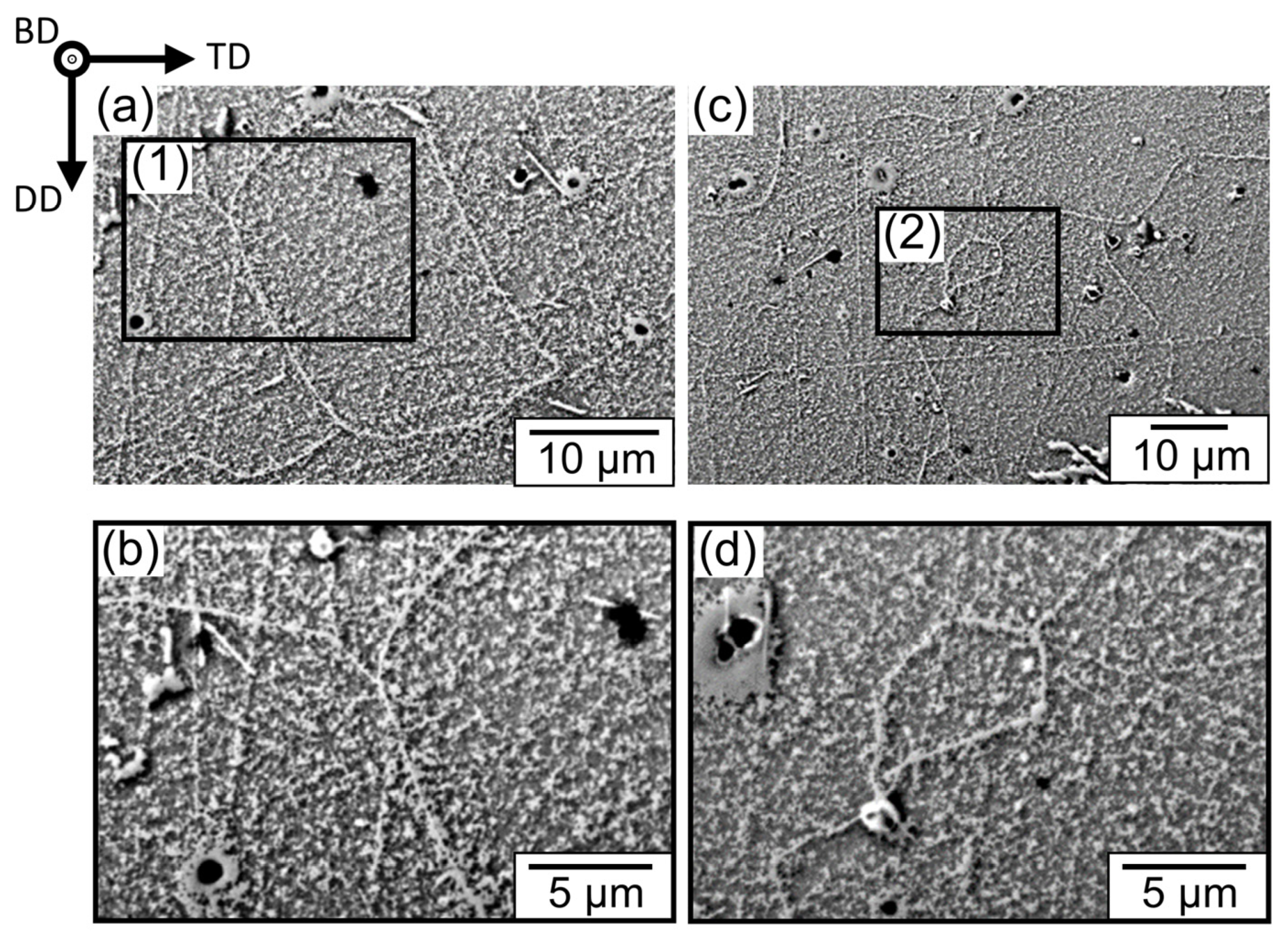
When the DD-TD section was investigated by SEM (Figure 6), subgrain structures could be identified. The subgrain structures indicate minor misorientations of the crystal lattice, resulting in the formation of small angle grain boundaries. Figure 6a shows a subgrain with a major axis of approx. 32 µm. Several grain boundary triple junctions originate from the subgrain, and one is shown in Figure 6b in detail. In addition to the large subgrains (Figure 6a), isolated smaller subgrains (overview in Figure 6c, enlargement in Figure 6d) with a major axis of 7–9 µm are also present in the grain interior. No dependence between the subgrain size and the size of the parent grain or the position in the parent grain were detected. The subgrain boundaries are characterized by a small γ phase seam. No enhanced growth of the γ phase, starting from the grain boundary inside the α grain, took place. Although the martensitic γ′ needles and the γ phase seam both appear in SEM to contrast with the same intensity and show morphologically a similar lateral spread, they differ significantly in their longitudinal expression. While the γ phase seams show irregular structures and the grain boundary angles do not follow any obvious regularity, the γ′ needles are characterized by their typical formation along lattice planes predetermined by the α matrix. Therefore, subgrain boundaries can be distinguished from martensitic γ′ needles.
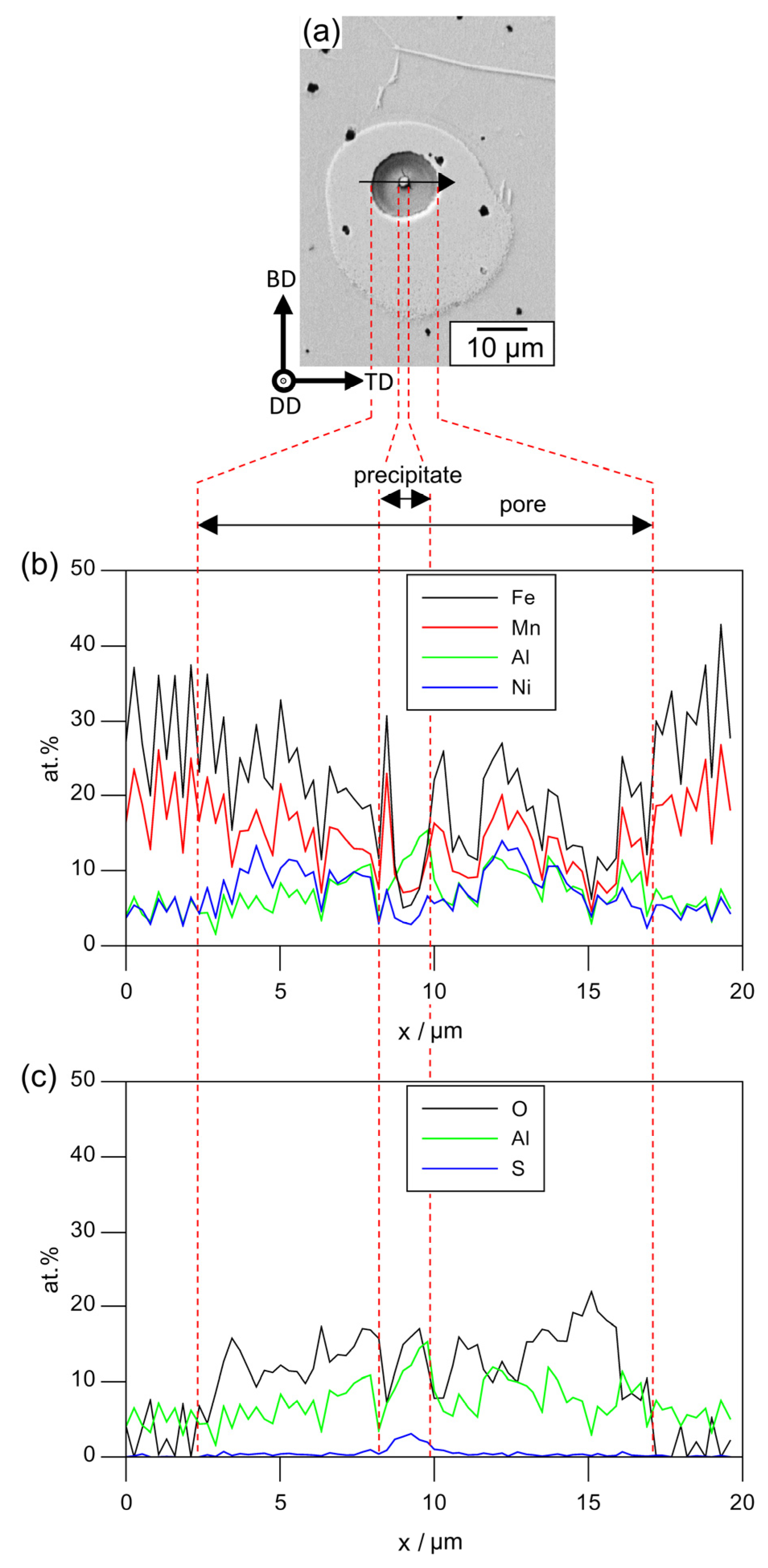
In both the OM and SEM images, precipitates can be identified within the α grains, which simultaneously lead to pore formation. In order to analyze the composition of the precipitates, EDS line scans were performed. Despite the absolute error of 2–5%, EDS data typically have much accuracy when relative changes are compared. Figure 7a shows a precipitated particle within a pore. The black arrow indicates the length and orientation of the EDS line scans. In Figure 7b, the change in concentration of the main alloying elements is plotted. While the Fe and Mn content decreases inside the pore, an increase in Al and Ni can be observed. The precipitation is characterized by an increase in Al content, while the amount of the other three main alloying elements decreases. When the minor elements O and S are taken into account (Figure 7c), an increase in content is also evident for oxygen at the pore. Sulphur, on the other hand, is only detected in the precipitate. The simultaneous increase in the Al and S content in the precipitate indicate that aluminium sulfide had formed. At the same time, an increased oxide formation in the pore becomes apparent. The influence of the pores and precipitates formed by segregation on the shape memory properties should be investigated in more detail, as these can suppress the reversible α→γ′→α transformation and act as pinning sites of the γ′ martensite.
3.3. X-ray Diffraction
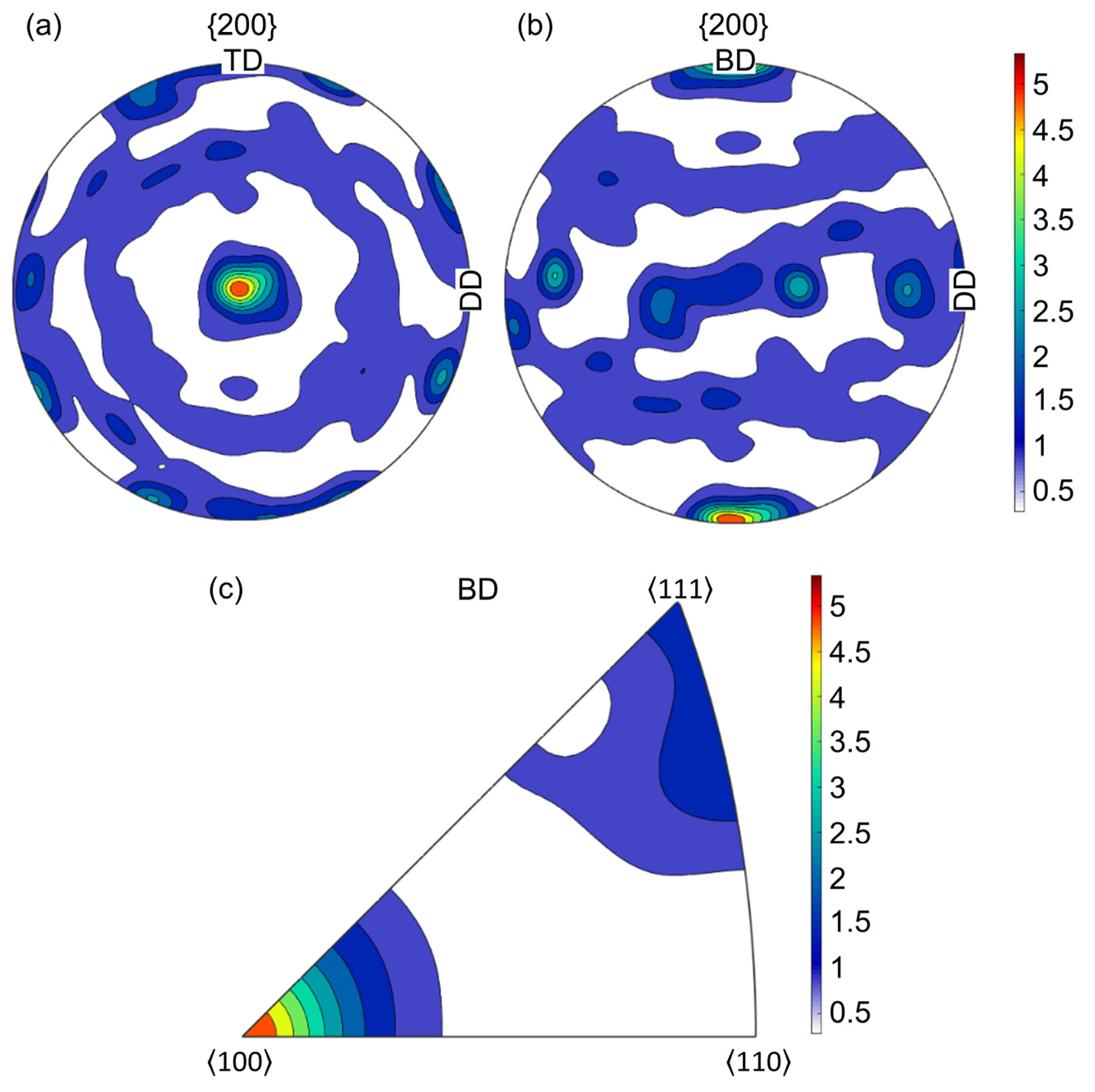
Since it was confirmed by OM that AM of FeMnAlNi by TIG-WAAM results in a preferred crystal growth in BD, texture measurements using XRD were carried out. When the DD-TD section was investigated, the smaller grain diameter compared to the grain diameter of the BD-TD section led to an increase in simultaneously observable grain orientations. By subsequently rotating the measured and recalculated pole figure, the frequently used viewing direction in TD was obtained. Figure 8 shows the recalculated pole figures of the {200} planes in BD (a) and TD (b) as well as the inverse pole figure in BD (c). When the pole figure of the {200} planes in BD is considered (Figure 8a), a preferred orientation of the crystals with respect to BD with only slight misorientations becomes apparent. The theoretically predominant 〈100〉 easy growth direction in bcc primarily solidifying alloys is only slightly tilted with respect to the BD. The preferred orientation, equivalent to the orientation with the maximum intensity when the ODF is considered, is defined by the Euler angles φ1 = 232°, Φ= 5° and φ2 = 14° (triclinic specimen symmetry). The bidirectional approach has thus led to a parallel alignment of the 〈100〉 and the BD. While in BD the {200} shows a clear maximum, in TD a significantly higher variance of the orientations occurs (Figure 8b). This is in agreement with the previously made assumption that the 〈100〉 in BD grows preferentially against the heat flux. Since no pronounced temperature gradient occurs in the DD-TD plane, no preferred growth direction can be observed. The competitive growth of individual grains therefore leads to the formation of high angle grain boundaries when grains with high misorientations collide. Already in [36,37], a strong dependence of the sample geometry and the texture formation was reported. While in [37] a loss of texture with increasing sample volume was observed, the TIG-WAAM process employed in the present study still shows a clear columnar texture despite the comparatively high sample volume. Due to the change in the manufacturing process, the significant increase in sample volume does not lead to a random orientation of the grains. Tseng et al. [23,24] have already shown that the crystallographic orientation regarding the load direction is decisive for the magnitude of the SME. According to theoretical calculations, for both the twinned and detwinned states, the transformation strain is highest in 〈100〉 and similar directions. So, a high transformation strain in BD can be predicted for crystallographic orientation of the TIG-WAAM fabricated FeMnAlNi sample. On the one hand, the grains show a low misorientation in BD, as shown by the concentrated maximum in Figure 8a, and on the other hand, preferential directions with high transformation strains are present in BD. The influence of the grain boundaries, which also run in BD, and the resulting intercrystalline stresses must be addressed in future investigations.
3.4. Thermomagnetization
The normalized electrical susceptibility in the temperature range from 125 K to 450 K is plotted in Figure 9. Different from the measurements of Omori et al. [12], a unique , , and cannot be determined for the TIG-WAAM fabricated FeMnAlNi alloy, nor is a clear hysteresis of magnetization formed. The low α/γ ratio of the specimen (as discussed previously) curtails the formation of a pronounced MT. Nevertheless, the decrease in the χ/χmax susceptibility indicates a thermally induced α→γ′ transformation, as the susceptibility decreases with the formation of the weak magnetic to antiferromagnetic γ′ phase at low temperatures. A Curie temperature of = 435 K was determined at the maximum of the susceptibility change |Δ(χ/χmax)/ΔT|, which deviates significantly from the values reported by Omori et al. for the solution treated state of polycrystalline Fe43.5Mn34Al15Ni7.5 ( = 390 K) and the aged state ( = 397 K) [12]. By ICP-OES, a decrease in the Mn content of the as-built state of approx. 5.3 at.% (cf. Table 1) was determined. is significantly affected by the Mn content and increases with decreasing content, as shown in [12]. Thus, Mn loss during the manufacturing process leads to an increase in . In addition to the loss of manganese, a loss of aluminium of 1.5 at.% was also observed after AM. While the Mn content significantly influences the , only a minor influence of Al on is reported in [12]. The loss of Mn and Al during TIG-WAAM could be counteracted by using higher alloyed filler material.
4. Conclusions
Industrially produced FeMn34Al15Ni7.5 was processed by additive manufacturing using TIG-WAAM. The microstructure, texture and thermomagnetization were investigated. The main results can be summarized as follows:
(1) A columnar texture with a grain length of up to 8 mm in BD was established. When the top layer is considered, a seam of γ phase had formed around the individual α grains along the grain boundaries. No large-scale γ precipitates occurred in the grain interior.
(2) An α→γ phase transformation occurred in the previously welded layers when a new layer was welded on top and a pronounced HAZ was formed. This led to a loss of the α fraction in the sample and to an unfavorable α/γ ratio for the SME. Nevertheless, the grain boundaries remained visible beyond several layers.
(3) When the DD-TD section at the level of the top layer is considered, areas with grains occupying a small average diameter of 65 µm and those with a larger average diameter of 1.2 mm were obtained. Grains with a larger diameter formed preferentially at the center of the specimens.
(4) Within the grains in the DD-TD section, subgrain structures can be observed surrounded by a fine γ phase seam. The subgrain structures indicate minor misorientations of the crystal lattice, resulting in the formation of small angle grain boundaries.
(5) Primarily formed γ grains can be distinguished from secondarily formed grains by their angular position regarding the BD, indicating diverging temperature–time paths and temperature gradients during the α→γ transformation.
(6) Due to conventional fabrication, impurities occur in the alloy, leading to the precipitation of aluminium sulfides.
(7) The 〈100〉 direction is near parallel to the BD (φ1 = 232°, Φ = 5°, φ2 = 14°). No clear preferred orientation occurs in TD and DD. According to [23,24], the preferred orientations in BD are likely to exhibit high transformation strain, both in twinned and detwinned states.
(8) No hysteresis was observed during the measurement of thermomagnetization, and the Curie temperature of = 435 K is higher than the Curie temperature determined by [12]. This is caused by the unfavorable α/γ ratio. Nevertheless, a decrease in χ/χmax due to the α→γ′ transformation occurred with falling temperature.
Processing the FeMnAlNi alloy by TIG-WAAM offers a promising route to achieving an anisotropic and textured polycrystalline material for use in civil engineering. Especially large-scale components with a pronounced texture are attainable. In future studies, the mechanical as well as the shape memory properties will be investigated.
Author Contributions
Conceptualization, V.F.V.; investigation, V.F.V.; writing—original draft preparation, V.F.V.; writing—review and editing, T.H. and H.J.M.; visualization, V.F.V.; supervision, H.J.M.; project administration, T.H.; funding acquisition, T.H. and H.J.M. All authors have read and agreed to the published version of the manuscript.
Funding
This research was funded by DEUTSCHE FORSCHUNGSGEMEINSCHAFT, grant number 401738767.
Data Availability Statement
Data are available from the corresponding author on reasonable request.
Acknowledgments
The material was processed by thyssenkrupp Steel Europe AG (Duisburg, Germany). The APC was funded by Open Access Fund of Leibniz Universität Hannover.
Conflicts of Interest
The authors declare no conflict of interest.
References
- Buehler, W.J.; Gilfrich, J.V.; Wiley, R.C. Effect of Low-Temperature Phase Changes on the Mechanical Properties of Alloys near Composition TiNi. J. Appl. Phys. 1963, 34, 1475–1477. [Google Scholar] [CrossRef]
- Miyazaki, S.; Ohmi, Y.; Otsuka, K.; Suzuki, Y. Characteristics of Deformation and Transformation Pseudoelasticity in Ti-Ni Alloys. Le J. Phys. Colloq. 1982, 43, 255–260. [Google Scholar] [CrossRef]
- Miyazaki, S.; Kimura, S.; Takei, F.; Miura, T.; Otsuka, K.; Suzuki, Y. Shape Memory Effect and Pseudoelasticity in a Ti-Ni Single Crystal. Scr. Metall. 1983, 17, 1057–1062. [Google Scholar] [CrossRef]
- Sehitoglu, H.; Jun, J.; Zhang, X.; Karaman, I.; Chumlyakov, Y.; Maier, H.J.; Gall, K. Shape memory and pseudoelastic behavior of 51.5% Ni–Ti single crystals in solutionized and overaged state. Acta Mater. 2001, 49, 3609–3620. [Google Scholar] [CrossRef]
- Hodgson, D.E.; Wu, M.H.; Biermann, R.J. Shape Memory Alloys. ASM Handb. 1990, 2, 897–902. [Google Scholar]
- Liu, Y.; Mahmud, A.; Kursawe, F.; Nam, T.H. Effect of pseudoelastic cycling on the Clausius—Clapeyron relation for stress-induced martensitic transformation in NiTi. J. Alloys Compd. 2008, 449, 82–87. [Google Scholar] [CrossRef]
- Liu, Y.; Yang, H. Strain dependence of the Clausius–Clapeyron relation for thermoelastic martensitic transformations in NiTi. Smart Mater. Struct. 2007, 16, 22–27. [Google Scholar] [CrossRef]
- Mohd Jani, J.; Leary, M.; Subic, A.; Gibson, M.A. A review of shape memory alloy research, applications and opportunities. Mater. Des. 2014, 56, 1078–1113. [Google Scholar] [CrossRef]
- Sato, A.; Chishima, E.; Soma, K.; Mori, T. Shape memory effect in γ⇄ϵ transformation in Fe-30Mn-1Si alloy single crystals. Acta Metall. 1982, 30, 1177–1183. [Google Scholar] [CrossRef]
- Wan, J.; Chen, S. Martensitic transformation and shape memory effect in Fe–Mn–Si based alloys. Curr. Opin. Solid State Mater. Sci. 2005, 9, 303–312. [Google Scholar] [CrossRef]
- Tanaka, Y.; Himuro, Y.; Kainuma, R.; Sutou, Y.; Omori, T.; Ishida, K. Ferrous Polycrystalline Shape-Memory Alloy Showing Huge Superelasticity. Science 2010, 327, 1488–1490. [Google Scholar] [CrossRef] [PubMed]
- Omori, T.; Ando, K.; Okano, M.; Xu, X.; Tanaka, Y.; Ohnuma, I.; Kainuma, R.; Ishida, K. Superelastic Effect in Polycrystalline Ferrous Alloys. Science 2011, 333, 68–71. [Google Scholar] [CrossRef] [PubMed]
- Ishida, K.; Shibuya, K.; Nishizawa, T. γ-Loops in Fe-Mn-V, Fe-Mn-Mo and Fe-Mn-Si Systems. J. Jpn. Inst. Met. 1973, 37, 1305–1313. [Google Scholar] [CrossRef] [Green Version]
- Ueland, S.M.; Chen, Y.; Schuh, C.A. Oligocrystalline Shape Memory Alloys. Adv. Funct. Mater. 2012, 22, 2094–2099. [Google Scholar] [CrossRef]
- Ueland, S.M.; Schuh, C.A. Superelasticity and fatigue in oligocrystalline shape memory alloy microwires. Acta Mater. 2012, 60, 282–292. [Google Scholar] [CrossRef]
- Ueland, S.M.; Schuh, C.A. Grain boundary and triple junction constraints during martensitic transformation in shape memory alloys. J. Appl. Phys. 2013, 114, 53503. [Google Scholar] [CrossRef]
- Xie, J.X.; Liu, J.L.; Huang, H.Y. Structure design of high-performance Cu based shape memory alloys. Rare Met. 2015, 34, 607–624. [Google Scholar] [CrossRef]
- Tseng, L.W. Microstructure and Superelastic Response of Iron based Shape Memory Alloy. Ph.D. Thesis, Texas A&M University: College Station, TX, USA, May 2015. [Google Scholar]
- Vollmer, M.; Segel, C.; Krooß, P.; Günther, J.; Tseng, L.W.; Karaman, I.; Weidner, A.; Biermann, H.; Niendorf, T. On the effect of gamma phase formation on the pseudoelastic performance of polycrystalline Fe-Mn-Al-Ni shape memory alloys. Scr. Mater. 2015, 108, 23–26. [Google Scholar] [CrossRef]
- Omori, T.; Okano, M.; Kainuma, R. Effect of grain size on superelasticity in Fe-Mn-Al-Ni shape memory alloy wire. APL Mater. 2013, 1, 032103. [Google Scholar] [CrossRef]
- Omori, T.; Iwaizako, H.; Kainuma, R. Abnormal grain growth induced by cyclic heat treatment in Fe-Mn-Al-Ni superelastic alloy. Mater. Des. 2016, 101, 263–269. [Google Scholar] [CrossRef]
- Tseng, L.W.; Ma, J.; Wang, S.J.; Karaman, I.; Kaya, M.; Luo, Z.P.; Chumlyakov, Y.I. Superelastic response of a single crystalline FeMnAlNi shape memory alloy under tension and compression. Acta Mater. 2015, 89, 374–383. [Google Scholar] [CrossRef]
- Tseng, L.W.; Ma, J.; Wang, S.J.; Karaman, I.; Chumlyakov, Y.I. Effects of crystallographic orientation on the superelastic response of FeMnAlNi single crystals. Scr. Mater. 2016, 116, 147–151. [Google Scholar] [CrossRef] [Green Version]
- Tseng, L.W.; Ma, J.; Chumlyakov, Y.I.; Karaman, I. Orientation dependence of superelasticity in FeMnAlNi single crystals under compression. Scr. Mater. 2019, 166, 48–52. [Google Scholar] [CrossRef]
- Ball, J.M.; James, R.D. Fine phase mixtures as minimizers of energy. Arch. Ration. Mech. Anal. 1987, 100, 13–52. [Google Scholar] [CrossRef]
- Saburi, T.; Nenno, S. The shape memory effect and related phenomena. Solid Solid Phase Transf. 1981, 1455–1479. [Google Scholar]
- DebRoy, T.; Wei, H.L.; Zuback, J.S.; Mukherjee, T.; Elmer, J.W.; Milewski, J.O.; Beese, A.M.; Wilson Heid, A.; De, A.; Zhang, W. Additive manufacturing of metallic components—Process, structure and properties. Prog. Mater. Sci. 2018, 92, 112–224. [Google Scholar] [CrossRef]
- Zhang, H.; Huang, J.; Liu, C.; Ma, Y.; Han, Y.; Xu, T.; Lu, J.; Fang, H. Fabricating Pyramidal Lattice Structures of 304 L Stainless Steel by Wire Arc Additive Manufacturing. Materials 2020, 13, 3482. [Google Scholar] [CrossRef] [PubMed]
- Costabile, G.; Fera, M.; Fruggiero, F.; Lambiase, A.; Pham, D. Cost models of additive manufacturing: A literature review. Int. J. Ind. Eng. Comput. 2017, 8, 263–283. [Google Scholar] [CrossRef]
- Thomas, D.S.; Gilbert, S.W. Costs and cost effectiveness of additive manufacturing. NIST Spec. Publ. 2014, 1176, 12. [Google Scholar]
- Hassel, T.; Carstensen, T. Properties and anisotropy behaviour of a nickel base alloy material produced by robot-based wire and arc additive manufacturing. Weld. World 2020, 64, 1921–1931. [Google Scholar] [CrossRef]
- Gokhale, N.P.; Kala, P.; Sharma, V. Thin-walled metal deposition with GTAW welding-based additive manufacturing process. J. Braz. Soc. Mech. Sci. Eng. 2019, 41, 569. [Google Scholar] [CrossRef]
- Gokhale, N.P.; Kala, P. Thermal analysis of TIG-WAAM based metal deposition process using finite element method. Mater. Today: Proc. 2021, 44, 453–459. [Google Scholar] [CrossRef]
- Helmer, H.; Bauereiß, A.; Singer, R.F.; Körner, C. Grain structure evolution in Inconel 718 during selective electron beam melting. Mater. Sci. Eng. A 2016, 668, 180–187. [Google Scholar] [CrossRef]
- Niendorf, T.; Brenne, F.; Schaper, M.; Riemer, A.; Leuders, S.; Reimche, W.; Schwarze, D.; Maier, H.J. Labelling additively manufactured parts by microstructural gradation-advanced copy-proof design. Rapid Prototyp. J. 2016, 22, 630–635. [Google Scholar] [CrossRef]
- Ewald, F.C.; Brenne, F.; Gustmann, T.; Vollmer, M.; Krooß, P.; Niendorf, T. Laser Powder Bed Fusion Processing of Fe-Mn-Al-Ni Shape Memory Alloy—On the Effect of Elevated Platform Temperatures. Metals 2021, 11, 185. [Google Scholar] [CrossRef]
- Niendorf, T.; Brenne, F.; Krooß, P.; Vollmer, M.; Günther, J.; Schwarze, D.; Biermann, H. Microstructural Evolution and Functional Properties of Fe-Mn-Al-Ni Shape Memory Alloy Processed by Selective Laser Melting. Met. Mater. Trans. A 2016, 47, 2569–2573. [Google Scholar] [CrossRef]
- Sun, S.H.; Koizumi, Y.; Saito, T.; Yamanaka, K.; Li, Y.P.; Cui, Y.; Chiba, A. Electron beam additive manufacturing of Inconel 718 alloy rods: Impact of build direction on microstructure and high-temperature tensile properties. Addit. Manuf. 2018, 23, 457–470. [Google Scholar] [CrossRef]
- Flemings, M.C. Solidification processing. Metall. Mater. Trans. B 1974, 5, 2121–2134. [Google Scholar] [CrossRef]
- Kurz, W.; Fisher, D.J. Fundamentals of Solidification, 4th ed.; Trans Tech Publications, Ltd.: Zurich, Switzerland, 1998. [Google Scholar]
- David, S.A.; Babu, S.S.; Vitek, J.M. Welding: Solidification and Microstructure. JOM 2003, 55, 14–20. [Google Scholar] [CrossRef]
- Schulze, G. Die Metallurgie des Schweißens: Eisenwerkstoffe-nichteisenmetallische Werkstoffe; Springer: Heidelberg, Germany; New York, NY, USA, 2010. [Google Scholar]
- Dinda, G.P.; Dasgupta, A.K.; Mazumder, J. Texture control during laser deposition of nickel based superalloy. Scr. Mater. 2012, 67, 503–506. [Google Scholar] [CrossRef]
Figure 1.
Grain orientation of the α-bcc phase as a function of the temperature gradient grad T (white arrow) and the welding direction WD (black arrow) for (a) unidirectional welding and (b) bidirectional welding; the structure is defined by the coordinate system containing building direction (BD), deposition direction (DD) and transverse direction (TD), respectively.

Figure 2.
OM images obtained of the polished and etched BD-TD section; (a) overview of the cross-section; magnifications of the top layer (1), middle section (2) and first layer (3) are shown in (b), (c,d), respectively; the sample coordinate system is defined by the building direction (BD), deposition direction (DD) and transverse direction (TD).

Figure 3.
OM images obtained from the polished and etched BD-DD section; (a) overview of the cross-section; (b) BD-DD cross-section with highlighted grains (red) and beginning of the HAZ (white) in several layers; the sample coordinate system is defined by the building direction (BD), deposition direction (DD) and transverse direction (TD).

Figure 4.
OM images obtained of the polished and etched DD-TD section; (a) overview of the cross-section; higher magnification detail of the area with small diameter grains (1) of approx. 65–180 µm is shown in (b) and of the larger diameter grains (2) up to 1.2 mm in (c); the sample coordinate system is defined by the building direction (BD), deposition direction (DD) and transverse direction (TD).

Figure 5.
SEM image of the polished and etched BD-TD section; (a) showing an overview of the transition to the HAZ and an adjacent grain boundary (GB); (b) interface between the primarily formed γ grains along the grain boundary and the secondarily formed γ grains in the grain interior; (c) higher magnification detail of (1) showing the interface between primarily and secondarily γ grains; (d) angles between the primarily γ grains (dashed lines indicate the orientation of the major axis) and the BD (ω1) and between the primarily and secondarily γ grains (ω2) are dotted; the sample coordinate system is defined by the building direction (BD), deposition direction (DD) and transverse direction (TD).

Figure 6.
SEM image of the polished and etched DD-TD section; (a) showing an overview of a subgrain (approx. 32 µm diameter) inside a large α grain and in (b) magnification of area (1) showing the triple junction grain boundary of the subgrain; (c) shows the grain interior of another large α grain with a small subgrain (7–9 µm diameter) and in (d) the subgrain from area (2) is shown; the sample coordinate system is defined by the building direction (BD), deposition direction (DD) and transverse direction (TD).

Figure 7.
Analysis of a pore and precipitate using EDS line scans; (a) SEM image of the pore and precipitate (black arrow indicating the length and orientation of the EDS line scans); (b,c) showing the distribution of the main alloying elements Fe, Mn, Al and Ni and selected minor elements (i.e., O, S).

Figure 8.
XRD texture analysis of the specimen prepared in the DD-TD plane; (a) showing the recalculated pole figure of the measured texture of the α-bcc {200} plane in BD; (b) recalculated and rotated pole figure of the measured α bcc {200}; (c) invers pole figure showing the preferred directions in BD.

Figure 9.
Normalized electrical susceptibility measured in the range from 125 K to 450 K.


Table 1.
Mean chemical composition of the filler material and the as-built state measured using ICP-OES.
Table 1.
Mean chemical composition of the filler material and the as-built state measured using ICP-OES.
| Specimen | Composition (at.%) | |||
|---|---|---|---|---|
| Mn | Al | Ni | Fe | |
| Filler material | 32.3 | 13.9 | 7.5 | balance |
| As-built | 28.7 | 13.5 | 7.3 | balance |
| Nominal | 34 | 15 | 7.5 | balance |
| Literature [12] | 34 | 15 | 7.5 | 43.5 |
Publisher’s Note: MDPI stays neutral with regard to jurisdictional claims in published maps and institutional affiliations. |
© 2022 by the authors. Licensee MDPI, Basel, Switzerland. This article is an open access article distributed under the terms and conditions of the Creative Commons Attribution (CC BY) license (https://creativecommons.org/licenses/by/4.0/).
Share and Cite
MDPI and ACS Style
Viebranz, V.F.; Hassel, T.; Maier, H.J. Microstructural Investigation of a FeMnAlNi Shape Memory Alloy Processed by Tungsten Inert Gas Wire and Arc Additive Manufacturing. Metals 2022, 12, 1731. https://doi.org/10.3390/met12101731
AMA Style
Viebranz VF, Hassel T, Maier HJ. Microstructural Investigation of a FeMnAlNi Shape Memory Alloy Processed by Tungsten Inert Gas Wire and Arc Additive Manufacturing. Metals. 2022; 12(10):1731. https://doi.org/10.3390/met12101731
Chicago/Turabian StyleViebranz, Vincent Fabian, Thomas Hassel, and Hans Jürgen Maier. 2022. "Microstructural Investigation of a FeMnAlNi Shape Memory Alloy Processed by Tungsten Inert Gas Wire and Arc Additive Manufacturing" Metals 12, no. 10: 1731. https://doi.org/10.3390/met12101731
Note that from the first issue of 2016, this journal uses article numbers instead of page numbers. See further details here.