Tuning the Morphology and Properties of Nanostructured Cu-ZnO Thin Films Using a Two-Step Sputtering Technique


1
Department of Chemistry, Konkuk University, Seoul 143-701, Korea
2
Department of Advanced Technology Fusion, Konkuk University, Seoul 143-701, Korea
*
Author to whom correspondence should be addressed.
Metals 2020, 10(4), 437; https://doi.org/10.3390/met10040437
Submission received: 10 February 2020
/
Revised: 18 March 2020
/
Accepted: 25 March 2020
/
Published: 27 March 2020
Abstract
:Zinc oxide (ZnO) is a wide-band-gap semiconductor that is promising for use as a transparent conductive oxide film. To date, to improve their optoelectrical properties, pristine ZnO films have been doped with metals using various techniques. In this study, nanostructured Cu-ZnO thin films were synthesized using a modified two-step radio frequency magnetron sputtering technique with separate ZnO and metallic Cu targets. Controlling the timing of the Cu/ZnO co-sputtering and ZnO-only sputtering steps afforded a significant change in the resulting nanostructures, such as uniform Cu-ZnO and broccoli-structured Cu-ZnO thin films. Using various measurement techniques, the influence of Cu doping was analyzed in detail. Furthermore, a crystal growth model for the formation of the broccoli-like clusters was suggested. The Cu-ZnO thin films synthesized using this technique demonstrate a highly improved conductivity with some loss in optical transmittance.
1. Introduction
Zinc oxide (ZnO) is considered a promising material for optoelectronics and laser applications owing to its wide band gap (3.1–3.3 eV) and high exciton binding energy (60 meV) [1,2,3]. In addition, its long-term stability, low cost, nontoxicity, and excellent optical and electrical properties make ZnO a promising candidate for photovoltaic applications [3,4]. The resistivity of intrinsic ZnO thin films is generally very high, up to ~105 Ωm [5] and >1011 Ωm [6] in the directions perpendicular and parallel to the substrate, respectively. Recently, this high resistivity has been applied in fields such as radiation detection [7,8], but to use ZnO in practical photovoltaic applications, the resistivity should be reduced by either creating intrinsic defects, such as oxygen vacancies or metal interstitials, or by introducing extrinsic dopants. ZnO thin films prepared by the former technique may become deoxidized, resulting in a higher resistivity; hence, the latter technique is more desirable for high-temperature applications [6,9].
Many groups have reported the influence on ZnO thin films of metal dopants, including In [10], Al [11,12,13,14], Fe [12,15], Mn [16], Mg [17], and Ga [12,18], to replace indium-doped tin oxide or fluorine-doped tin oxide [1,3]. One promising dopant is Cu, which has been reported to show enhanced properties such as higher conductivity [19], diluted magnetic properties [15], and improved crystal quality [20]. To achieve uniform, high-quality Cu-doped ZnO films, sputtering has been highlighted as one of the most promising techniques. Various sputtering sources have been tested including Cu-attached Zn metal [19,21,22,23], two separate metals [24], ZnO and metallic Cu [25,26], and pre-synthesized Cu-doped ZnO [27]. In radio frequency (RF)/direct current (DC) co-sputtering and/or sequential sputtering, the use of two separate sources has been proven to be effective [25,28]. This approach has resulted in a decrease in crystal orientation [22], shrinkage of lattice constants [22,27], reduction in band gap [23,28], and broadening of Raman peaks [23,24]. In these previous reports, however, the diverse processing parameters were not controlled; only the sputtering ratio of the two sources has been considered using single-step sputtering.
Here, we report the properties of Cu-doped ZnO thin films synthesized by a modified two-step RF magnetron sputtering technique. By using both Cu and ZnO sources, the films were sputtered through a two-step process: co-sputtering of both Cu and ZnO sources and sputtering of ZnO alone. Although this method deviates from the standard technique, no such attempts have been reported, and the technique is particularly useful for evaluating the solubility limit of Cu and adjusting the nanostructure. By controlling the time ratios between the two steps, the Cu contents in the resulting Cu-ZnO thin films could be controlled effectively to yield a uniform Cu-ZnO thin film as well as a unique broccoli-like nanostructured film. A suitable model is suggested to describe the origin of this unique broccoli-like structure. Furthermore, to explain the properties of the sputtered Cu-ZnO thin films and the unique growth mechanism, various optical, structural, and electrical observations were performed.
2. Materials and Methods
Soda lime glass 5 cm × 5 cm in size (iTASCO, Seoul, Korea) was used as a substrate for ZnO sputtering. The substrates were washed with a soap solution followed by ultrasonic cleaning in acetone, isopropyl alcohol, and deionized water. Finally, they were dried with nitrogen gas. ZnO (99.99%) and Cu (99.999%) targets with diameters of 5.08 cm (2 in.) and thicknesses of 0.635 cm (0.25 in.) (iTASCO, Seoul, Korea) served as the RF magnetron sputtering sources and were loaded separately. The base and working pressure were maintained at 9 × 10⁻⁷ mbar and 5 × 10⁻⁴ mbar, respectively. The targets were pre-sputtered with argon plasma for 10 min to remove surface contamination and maintain the system stability. With the two separate sources (2 in. targets) of ZnO and Cu metal, we terminated the Cu sputtering step after a specific period of co-sputtering, while ZnO sputtering was maintained throughout. During this process, the Ar flow was maintained at 4.55 sccm, and the substrate temperature was set to 150 °C. The substrates were rotated at a speed of 15 rpm to ensure thickness uniformity. The RF power for the ZnO and Cu sources was maintained at 50 W (13.6 MHz) throughout the entire deposition process. The sputter system and the processing parameters are indicated in Figure S1. The total deposition time was kept at 40 min, and the Cu sputtering power turned off at 1, 2, 5, or 10 min. Accordingly, the Cu-ZnO films obtained with different Cu sputtering periods are referred to hereafter as Cx, where x denotes the Cu power shut-off time (x = 0, 1, 2, 5, and 10 min) during the co-sputtering of Cu and ZnO; i.e., C0 and C1 denote ZnO films with no co-sputtering period (ZnO-only sputtering) and co-sputtering for 1 min, respectively. The deposited samples were then annealed in air at 400 °C for 1 h. The heating and cooling rates were maintained at 12 °C/min to avoid cracking of the films.
The thickness of the samples was measured using a stylus thickness profilometer, and the crystal structure of each film was measured using an X-ray diffraction (XRD) (RINT 2500, Rigaku, Tokyo, Japan) using the CuKα radiation. Optical measurements of the samples were carried out using a UV-vis-NIR spectrophotometer (Cary 500, Varian, Markham. ON, Canada), and surface morphology and compositional analyses were carried out using a scanning electron microscope (SEM) and energy-dispersive X-ray (EDX) system (JSM 700F, JEOL, Tokyo, Japan). The Raman spectra of each sample were obtained at room temperature using a Raman micro-spectroscopy system (Nanofinder 30, Tokyo Instruments, Tokyo, Japan) with a 633 nm He-Ne laser vertically irradiated onto the sample surface. Conductivity measurements were carried out with the four-point probe method.
3. Results and Discussion
3.1. XRD Analysis
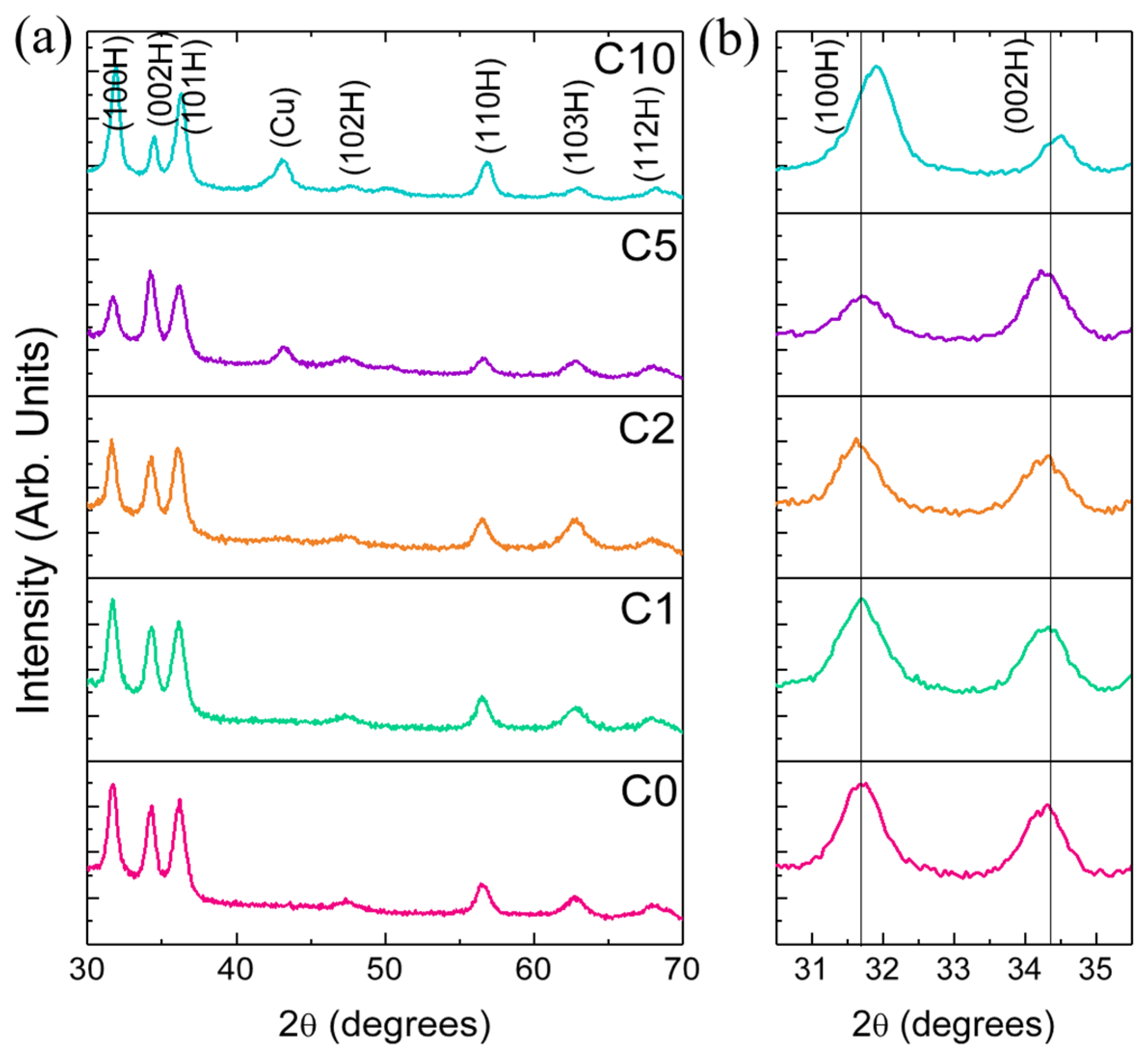
The XRD patterns of the Cx thin films after air annealing are shown in Figure 1. The crystal structure of the thin films was indexed to the hexagonal structure (JCPDS No. 79-0208). Both the C0 (ZnO-only sputtering) and C1 (1 min co-sputtering) thin films exhibited only pure ZnO phases. In the C2 pattern, a trace of an additional Cu-metal peak at 2θ of 43.23° was observed, which increased in intensity in the C5 and C10 patterns. Among the Cu compounds, the diffraction of the (111) planes of cubic Cu metal at 43.23° was a good match (JCPDS No. 04-0836). This means Cu atoms in the high-x films (C5 and C10) not only acted as dopants but also formed embedded Cu clusters, which agrees well with previous work [23]. It should be noted that a noticeable shift to higher diffraction angles occurred for both the (100H) and (002H) peaks in the C10 pattern; this indicates a smaller lattice constant, which induced a different internal strain in C10 than in the other thin films.
3.2. SEM/EDX Analysis
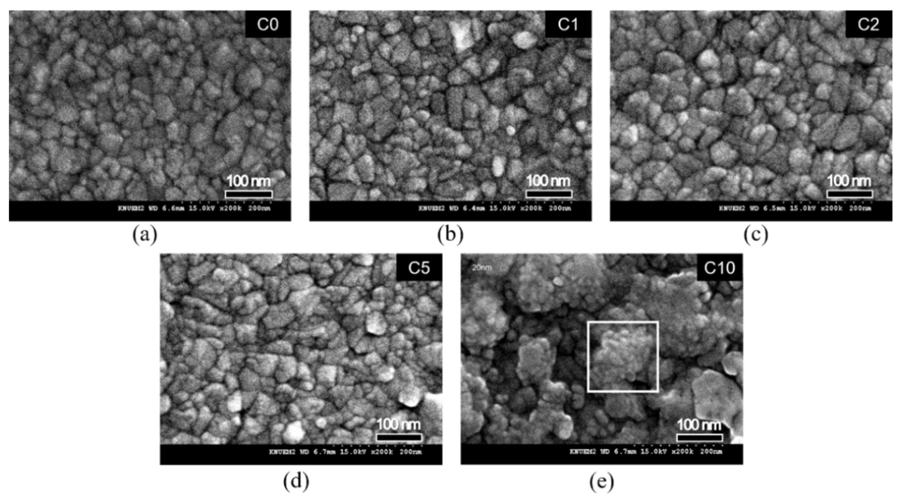
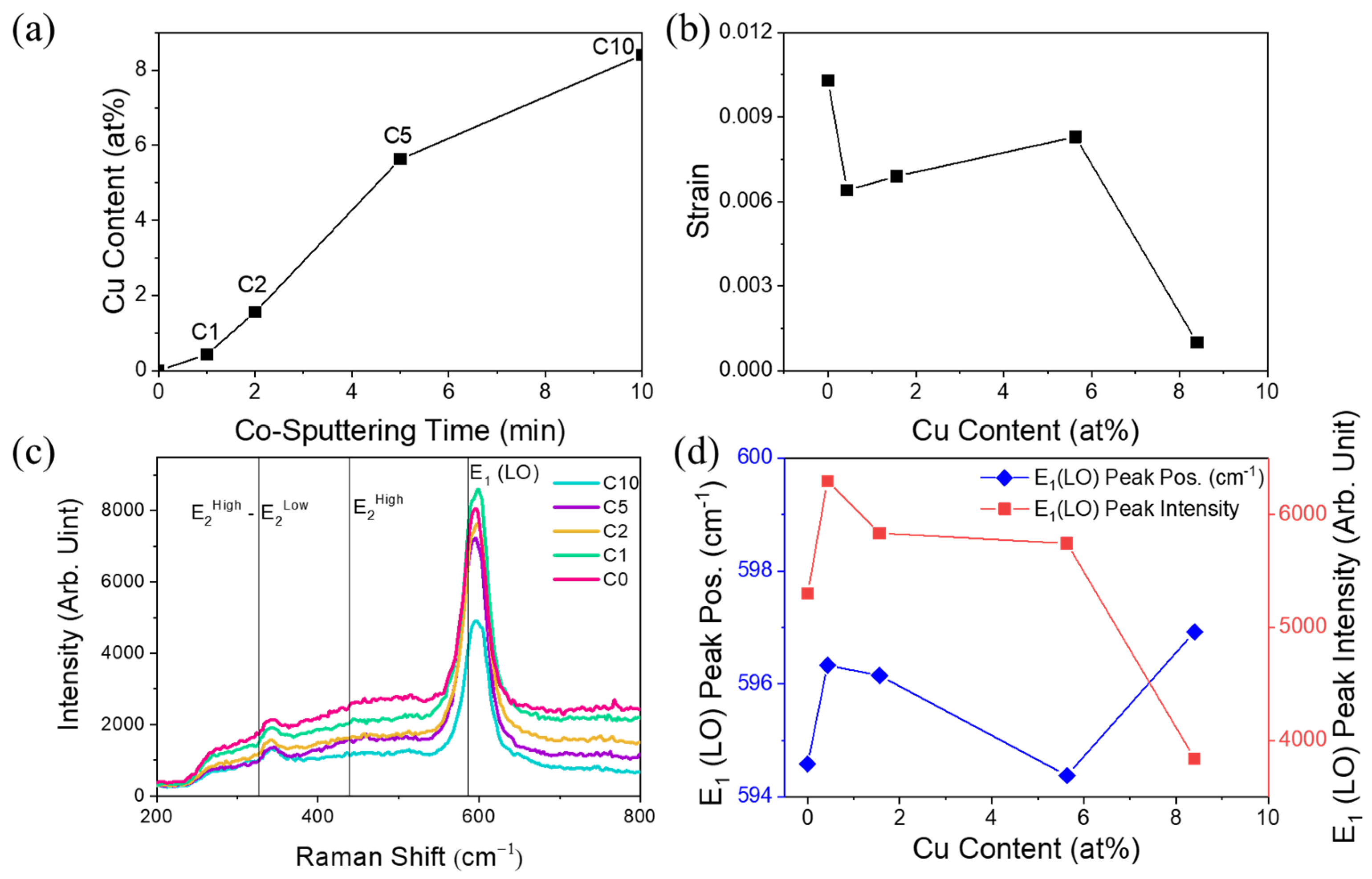
The field emission SEM micrographs of each sample are shown in Figure 2. In the C0 and low-x films (C1 and C2), comparatively homogeneous grains were observed. In the high-x films (C5 and C10), however, small primary grains were assembled to form large clusters. Particularly, in C10, broccoli-like clusters were found, meaning that different grain growth kinetics were involved in the high-x films. In general, morphologies showing broccoli-like clusters have been found in washed Ag-doped ZnO [29] and solution-processed La-doped ZnO [30]. Thus, it is interesting that C10 showed a similar morphology despite being synthesized from a completely different deposition process. Meanwhile, a similar nanostructure was reported when ZnO was sputtered onto Cu metal [31], suggesting that the formation of broccoli-like clusters was closely related to the internally isolated Cu present in the high-x films. The presence of Cu in the high-x films was confirmed by the above-discussed XRD analysis. To characterize the Cu content in each Cx film, EDX measurements were carried out. As no double layers were detected in the cross-sectional SEM images shown in Figure S2, the atomic ratio of Cu atoms could be determined from the EDX spectra. The results are shown in Figure 3a. The EDX spectra showed a nearly linear dependence of Cu content on time, where approximately 0.8% Cu was mixed into the ZnO matrix for each minute of Cu co-sputtering.
3.3. Williamson-Hall Analysis
To calculate the internal strain of each film from the XRD spectra, Williamson-Hall (W-H) analysis was performed [32,33]. The strain in the Cx films can be calculated from the full-width at half-maximum (FWHM) of each XRD peak using the following equations:
Here, βTotal is the FWHM of each XRD peak, λ; is the incident X-ray wavelength (Cu-Kα, 1.54 Å), θ is the diffraction angle, t is the crystal size, and ε is the strain corresponding to the target peak. The strain can be obtained from the slope of the linear-fitted plot of βcosθ versus 4sinθ. Seven XRD peaks of ZnO, as indicated in Figure 1a, were selected for this analysis. Linear fitting was performed using the least squares method, from which the strain of each film was obtained. These plots are shown in Figure S3, and the corresponding strain values are presented in Figure 3b. A high strain was calculated for pristine ZnO (C0). In general, strain in such films is mainly due to either a lattice mismatch between the film and substrate or the internal film structure. Because the glass substrate is an amorphous phase, strain arising from a lattice mismatch can be ignored. Thus, the initially high strain in the pristine ZnO film might be attributable to the internal structure of ZnO films, which will be discussed later. In general, Cu dopant atoms/ions can deform (relax) the crystal by substituting parent atoms (sitting in grain boundaries), which causes the formation (relaxation) of strain. In the C10 film with the highest Cu content, the lattice strain decreased significantly compared with that in C5. Therefore, this phenomenon could be explained by the presence of excess Cu dopants located at grain boundaries in C10, which may relax the increased strain.
3.4. Raman Analysis
To study their structural properties in greater detail, Raman analysis was performed on the ZnO thin films in the region of 200–800 cm−1 to observe the primary modes. The Raman-active spectra of each sample are depicted in Figure 3c. All samples showed two distinct peaks: the E2High−E2Low mode at approximately 344 cm−1 and the E1 (LO) mode at approximately 596 cm−1, which are similar to previous reports [34,35]. As the doping rate changed, the intensity and position of the E1 (LO) peak changed slightly. Though many previous studies have found that the E2High mode is the major peak in hexagonal ZnO [12,16,19,34,35,36,37,38], we could only observe its trace in the E2High−E2Low mode. In würtzite ZnO, the E2High peak is related to the vibration of O atoms, whereas E1 (LO), the most intense peak in our measured spectra, is related to the vibration of Zn atoms [39]. This means that the C0 (pristine ZnO) film has severe oxygen deficiency, which causes compressive deformation. This manifests as a substantial blue-shift in both the E2High−E2Low and E1 (LO) peaks, which are centered at approximately 330–340 cm−1 and 580–590 cm−1, respectively, compared with those observed in other studies. These oxygen vacancies intensify the E1 (LO) peak [35,40], and thus the intensity will decrease with fewer oxygen vacancies.
To obtain quantitative data, the E1 (LO) peak position and intensity were analyzed and are depicted in Figure 3d, where the background signal was eliminated using the asymmetric least squares smoothing method. By doing so, the trace of E2High was removed from the E1 (LO) peak to obtain the relative intensities of the E2High and E1 (LO) peaks, which are related to the oxygen vacancies [35,40]. The peak position, which shifts according to compressive strain, was slightly different from the strain calculated by the W-H method, but these differences were insignificant compared with the massive blue-shift observed in the E1 (LO) peak of all samples. The C5 peak had a similar intensity to that of C2, while C10 had the lowest intensity. This implies that Cu-ZnO films with higher Cu contents have fewer oxygen vacancies, which might cause the lower compressive strain indicated by the W-H plots.
3.5. UV-Vis Analysis
The optical absorbance and transmission spectra of each sample are shown in Figure 4a. C0 and C1 showed absorbances of less than 0.2 in the visible and UV range, which increased significantly with co-sputtering time. Finally, the absorbance of C10 is over 0.5 for the entire visible light spectrum.
The band gap of each thin film was calculated from the optical absorbance measurements using
where is the absorption coefficient, is the incident photon energy, Eg is the optical band gap, A is a constant, and n is 1/2 or 2 for direct or indirect allowed bands, respectively. Crystalline ZnO is known to be a direct band gap material, and so n = ½ was used. The band gap can be determined by extending the linear portion of the versus ()2 plot, called the Tauc plot, to the x-axis [41,42].
The absorption coefficient was calculated using the measured thickness of each sample shown in Table S1. The optical band gaps of the different samples are shown in Figure 4b. Pristine ZnO (C0), showed a bandgap of 3.26 eV and had no other absorption edge. In contrast, in the co-sputtered samples, there was another absorption edge located at 1–2 eV. This Cu-related edge in the high-x films was observed in some previous works but was not analyzed [23]. Considering its position, the Cu-related edge corresponds to CuO crystals, which have a band gap of approximately 1.2 eV [43] but were not detected by XRD due to their low content. In addition, as the Cu content increased, the background absorption across the entire region increased. This may arise from the metallic Cu observed in the XRD measurements, which blocked most visible light.
3.6. Electrical Conductivity Analysis
The electrical conductivities of all samples were measured with the four-point method and are shown in Table 1. The conductivity of the pristine ZnO thin film, C0, is 8.8 × 10⁻⁵ Ω−1cm−1, which decreased to 1.9 × 10⁻³ Ω−1cm−1 for C1 and 3.3 × 10⁻⁵ Ω−1cm−1 for C2, then increased by 100 times for C5 and C10. In co-sputtered ZnO, theoretically, Zni0, Vo0, VZn2−, Zni+, and the 3d state of Cu2+ are known to be donor centers, and VZn2−, Vo+, and the h state of Cu+ are acceptor centers [44]. It is commonly believed that divalent Cu ions enter the crystal structure by substituting Zn [45]. At low doping profiles, Cu may occupy the Vzn2− vacancies, which behave as donor centers, resulting in a decreased conductivity. At higher doping concentrations, the conductivity increased slightly, suggesting an increase in donor centers. C10, which had excess Cu, was shown in previous sections to have much fewer oxygen vacancies, which are donor centers. Thus, only the 3d state of doped Cu2+ ions could explain this increase. In addition, metallic Cu at the grain boundary could change the electron transport mechanism, increasing conductivity [46]. Based on the XRD data, there was a significant increase in the intensity of the Cu-related peak for ZnO films with higher Cu doping contents. This may explain why C5 and C10 had much higher conductivities than C1 and C2, which had lower Cu contents.
3.7. Crystal Growth Mechanism
From the analyses discussed in previous sections, the crystal growth dynamics of Cu co-sputtered ZnO could be suggested. The Raman spectra indicated a massive amount of defects, especially oxygen vacancies, and the conductivity data suggested interactions between Cu and defects in the ZnO matrix. The XRD spectra indicated that, at short co-sputtering times, all the doped Cu was located within the ZnO lattice to form solid solutions (C1 and C2), while at longer co-sputtering times, Cu formed isolated metallic Cu at grain boundaries (C5 and C10). It should be noted that because ZnO and Cu targets were used as sputtering sources, the supplied oxygen was insufficient to oxidize all metal atoms, resulting in unoxidized Cu. The ionization energy of Cu is lower than that of Zn, and thus the formation of ZnO and metallic Cu is more likely than the formation of CuO and metallic Zn during annealing in air. Furthermore, according to Wang et al., ZnO cannot be uniformly sputtered onto a Cu metal surface as it instead forms heterogeneous clusters [31]. This strongly suggests that the oxidization preference for ZnO in this study was high enough to induce clustered ZnO formation around isolated Cu surfaces.
Figure 5 illustrates the proposed model for the crystal growth of Cu-ZnO films and formation of broccoli-like nanostructures. If co-sputtering ceased after a short Cu sputtering period, further ZnO-only sputtering induced uniform Cu-ZnO microstructures. With longer co-sputtering periods, on the other hand, isolated metallic Cu clusters formed due to preferential oxidization, which partially covered the ZnO films. Such Cu clusters induced heterogeneous nucleation along grain boundaries, forming smaller, disoriented secondary ZnO crystals. Depending on the co-sputtering period, this effect could occur repeatedly on the boundary area of each crystal, causing these small grains to grow during the ZnO-only sputtering stage. This model explains the origin of the broccoli-like nanostructures.
4. Conclusions
In this study, using a modified two-step RF magnetron sputtering approach, Cu-ZnO thin films with various Cu contents were prepared using separate Cu metal and ZnO targets. SEM analysis showed that the pristine ZnO film had a homogeneous microstructure, whereas the highly Cu-doped ZnO film had a nanocrystalline broccoli-like morphology, which was explained by a crystal growth model. The XRD measurements revealed that the ZnO films were in a hexagonal phase, and the peaks shifted to higher diffraction angles with increasing Cu content. Using the W-H method, the relationship between strain and Cu doping was discussed, and interesting properties such as high conductivity improvement, reduced strains, changes in Raman responses, and band gap shifts were analyzed. Optical absorption studies showed that the transmission of the samples decreased considerably upon increasing the Cu content, and there was also a considerable reduction in the band gap. Finally, a crystal growth mechanism for the co-sputtered Cu-ZnO films was proposed that agreed with the observed properties. Cu-ZnO thin films synthesized using the proposed modified two-step sputtering technique exhibit a highly improved conductivity with some loss in optical transmittance.
Supplementary Materials
The following are available online at https://www.mdpi.com/2075-4701/10/4/437/s1. Figure S1: Detail illustration about dual-source RF magnetron sputtering system. Figure S2: Cross sectional SEM images of (a) C0, (b) C1, (c) C2, (d) C5, and (e) C10. There is no double layer detected in every thin film. Figure S3: Williamson-Hall plot of each sample. Seven XRD peaks of C0 (a), C1 (b), (c) C2, (d) C5, and (e) C10 were picked and linear-fitted using the least-square method. Table S1: Layer thickness measured using the stylus surface profilometer.
Author Contributions
Conceptualization and writing—original draft preparation, J.-H.L. and M.-J.L.; methodology, J.-H.L. and M.-J.L.; validation, M.-J.L.; formal analysis, J.-H.L., K.C.W., and M.-J.L.; investigation, M.-J.L.; resources, J.-H.L. and M.-J.L.; data curation, J.-H.L., K.O., and K.J.; writing—original draft preparation, J.-H.L. and M.-J.L.; writing—review and editing, M.-J.L. All authors have read and agreed to the published version of the manuscript.
Funding
This study was funded by Konkuk University.
Acknowledgments
This study was supported by Konkuk University in 2016.
Conflicts of Interest
The authors declare no conflict of interest.
References
- Tan, S.T.; Sun, X.W.; Zhang, X.H.; Chua, S.J.; Chen, B.J.; Teo, C.C. Cluster coarsening in zinc oxide thin films by postgrowth annealing. J. Appl. Phys. 2006, 100, 033502. [Google Scholar] [CrossRef]
- Chen, M.; Pei, Z.L.; Sun, C.; Wen, L.S.; Wang, X. Formation of Al-doped ZnO films by dc magnetron reactive sputtering. Mater. Lett. 2001, 48, 194–198. [Google Scholar] [CrossRef]
- Özgür, Ü.; Alivov, Y.I.; Liu, C.; Teke, A.; Reshchikov, M.A.; Doǧan, S.; Avrutin, V.; Cho, S.J.; Morko̧, H. A comprehensive review of ZnO materials and devices. J. Appl. Phys. 2005, 98, 11. [Google Scholar] [CrossRef] [Green Version]
- Gupta, K.M.; Gupta, N. Recent Advances in Semiconducting Materials and Devices; Springer: Cham, Switzerland, 2015; Volume 80, pp. 531–562. [Google Scholar]
- Chen, J.J.; Gao, Y.; Zeng, F.; Li, D.M.; Pan, F. Effect of sputtering oxygen partial pressures on structure and physical properties of high resistivity ZnO films. Appl. Surf. Sci. 2004, 223, 318–329. [Google Scholar] [CrossRef]
- Blom, F.R.; van de Pol, F.C.M.; Bauhuis, G.; Popma, T.J.A. RF planar magnetron sputtered ZnO films II: Electrical properties. Thin Solid Films 1991, 204, 365–376. [Google Scholar] [CrossRef] [Green Version]
- Zhou, L.; Huang, Z.; Zhao, X.; He, Y.; Chen, L.; Xu, M.; Zhao, K.; Zhang, S.; Ouyang, X. A High-Resistivity ZnO Film-Based Photoconductive X-Ray Detector. IEEE Photonics Technol. Lett. 2019, 31, 365–368. [Google Scholar] [CrossRef]
- Zhao, X.; Chen, L.; He, Y.; Liu, J.; Peng, W.; Huang, Z.; Qi, X.; Pan, Z.; Zhang, W.; Zhang, Z.; et al. Nanosecond X-ray detector based on high resistivity ZnO single crystal semiconductor. Appl. Phys. Lett. 2016, 108, 171103. [Google Scholar] [CrossRef]
- Ellmer, K. Resistivity of polycrystalline zinc oxide films: Current status and physical limit. J. Phys. D. Appl. Phys. 2001, 34, 3097–3108. [Google Scholar] [CrossRef]
- Jeong, J.A.; Choi, K.H.; Bae, J.H.; Moon, J.M.; Jeong, S.W.; Kim, I.; Kim, H.K.; Yi, M.S. Electrical, optical, and structural properties of ITO co-sputtered IZO films by dual target magnetron sputtering. J. Electroceramics 2009, 23, 361–366. [Google Scholar] [CrossRef]
- Kim, Y.S.; Tai, W.P. Electrical and optical properties of Al-doped ZnO thin films by sol-gel process. Appl. Surf. Sci. 2007, 253, 4911–4916. [Google Scholar] [CrossRef]
- Bundesmann, C.; Ashkenov, N.; Schubert, M.; Spemann, D.; Butz, T.; Kaidashev, E.M.; Lorenz, M.; Grundmann, M. Raman scattering in ZnO thin films doped with Fe, Sb, Al, Ga, and Li. Appl. Phys. Lett. 2003, 83, 1974–1976. [Google Scholar] [CrossRef]
- Meza, D.; Cruz, A.; Morales-Vilches, A.B.; Korte, L.; Stannowski, B. Aluminum-doped zinc oxide as front electrode for rear emitter silicon heterojunction solar cells with high efficiency. Appl. Sci. 2019, 9, 862. [Google Scholar] [CrossRef] [Green Version]
- Ji, X.; Song, J.; Wu, T.; Tian, Y.; Han, B.; Liu, X.; Wang, H.; Gui, Y.; Ding, Y.; Wang, Y. Solar Energy Materials and Solar Cells Fabrication of high-performance F and Al co-doped ZnO transparent conductive fi lms for use in perovskite solar cells. Sol. Energy Mater. Sol. Cells 2019, 190, 6–11. [Google Scholar] [CrossRef]
- Zhang, H.W.; Wei, Z.R.; Li, Z.Q.; Dong, G.Y. Room-temperature ferromagnetism in Fe-doped, Fe- and Cu-codoped ZnO diluted magnetic semiconductor. Mater. Lett. 2007, 61, 3605–3607. [Google Scholar] [CrossRef]
- Yang, L.W.; Wu, X.L.; Huang, G.S.; Qiu, T.; Yang, Y.M. In situ synthesis of Mn-doped ZnO multileg nanostructures and Mn-related Raman vibration. J. Appl. Phys. 2005, 97, 1–4. [Google Scholar] [CrossRef]
- Loeza-Poot, M.; Mis-Fernández, R.; Rimmaudo, I.; Camacho-Espinosa, E.; Peña, J.L. Novel sputtering method to obtain wide band gap and low resistivity in as-deposited magnesium doped zinc oxide films. Mater. Sci. Semicond. Process. 2019, 104, 104646. [Google Scholar] [CrossRef]
- Chen, H.; Du Pasquier, A.; Saraf, G.; Zhong, J.; Lu, Y. Dye-sensitized solar cells using ZnO nanotips and Ga-doped ZnO films. Semicond. Sci. Technol. 2008, 23, 045004. [Google Scholar] [CrossRef]
- Wang, X.B.; Song, C.; Geng, K.W.; Zeng, F.; Pan, F. Photoluminescence and Raman scattering of Cu-doped ZnO films prepared by magnetron sputtering. Appl. Surf. Sci. 2007, 253, 6905–6909. [Google Scholar] [CrossRef]
- Al-Khanbashi, H.A.; Shirbeeny, W.; Al-Ghamdi, A.A.; Bronstein, L.M.; Mahmoud, W.E. Development of highly conductive and transparent copper doped zinc oxide thin films via 2-methoxyethanol modified sol-gel dip-coating technique. Ceram. Int. 2014, 40, 1927–1932. [Google Scholar] [CrossRef]
- Ma, L.; Ma, S.; Chen, H.; Ai, X.; Huang, X. Microstructures and optical properties of Cu-doped ZnO films prepared by radio frequency reactive magnetron sputtering. Appl. Surf. Sci. 2011, 257, 10036–10041. [Google Scholar] [CrossRef]
- Peng, X.; Xu, J.; Zang, H.; Wang, B.; Wang, Z. Structural and PL properties of Cu-doped ZnO films. J. Lumin. 2008, 128, 297–300. [Google Scholar] [CrossRef]
- Agarwal, D.C.; Singh, U.B.; Gupta, S.; Singhal, R.; Kulriya, P.K.; Singh, F.; Tripathi, A.; Singh, J.; Joshi, U.S.; Avasthi, D.K. Enhanced room temperature ferromagnetism and green photoluminescence in Cu doped ZnO thin film synthesised by neutral beam sputtering. Sci. Rep. 2019, 9, 1–12. [Google Scholar] [CrossRef] [PubMed] [Green Version]
- Sudakar, C.; Thakur, J.S.; Lawes, G.; Naik, R.; Naik, V.M. Ferromagnetism induced by planar nanoscale CuO inclusions in Cu-doped ZnO thin films. Phys. Rev. B Condens. Matter Mater. Phys. 2007, 75, 1–6. [Google Scholar] [CrossRef]
- Liu, Y.; Liu, H.; Yu, Y.; Wang, Q.; Li, Y.; Wang, Z. Structural and optical properties of ZnO thin films with heavy Cu-doping prepared by magnetron co-sputtering. Mater. Lett. 2015, 143, 319–321. [Google Scholar] [CrossRef]
- Jilani, A.; Othman, M.H.D.; Ansari, M.O.; Oves, M.; Hussain, S.Z.; Khan, I.U.; Abdel-wahab, M.S. Structural and optical characteristics, and bacterial decolonization studies on non-reactive RF sputtered Cu–ZnO@ graphene based nanoparticles thin films. J. Mater. Sci. 2019, 54, 6515–6529. [Google Scholar] [CrossRef]
- Sung, N.E.; Kang, S.W.; Shin, H.J.; Lee, H.K.; Lee, I.J. Cu doping effects on the electronic and optical properties of Cu-doped ZnO thin films fabricated by radio frequency sputtering. Thin Solid Films 2013, 547, 285–288. [Google Scholar] [CrossRef]
- Sreedhar, A.; Kwon, J.H.; Yi, J.; Kim, J.S.; Gwag, J.S. Enhanced photoluminescence properties of Cu-doped ZnO thin films deposited by simultaneous RF and DC magnetron sputtering. Mater. Sci. Semicond. Process. 2016, 49, 8–14. [Google Scholar] [CrossRef]
- Abd, H. 3D hyperbranched heterostructures of Ag nanocrystals-decorated ZnO nanopillars: Controlled growth and characterization of the optical properties. CrystEngComm 2017, 19, 5591–5603. [Google Scholar]
- Jagtap, R.M.; Kshirsagar, D.R.; Khire, V.H.; Pardeshi, S.K. Facile fabrication of porous La doped ZnO granular nanocrystallites and their catalytic evaluation towards thermal decomposition of ammonium perchlorate. J. Solid State Chem. 2019, 276, 194–204. [Google Scholar] [CrossRef]
- Wang, Y.P.; Lu, J.G.; Bie, X.; Ye, Z.Z.; Li, X.; Song, D.; Zhao, X.Y.; Ye, W.Y. Transparent conductive and near-infrared reflective Cu-based Al-doped ZnO multilayer films grown by magnetron sputtering at room temperature. Appl. Surf. Sci. 2011, 257, 5966–5971. [Google Scholar] [CrossRef]
- Prabhu, Y.; Rao, K.; Kumar, V.; Kumari, B. X-Ray Analysis by Williamson-Hall and Size-Strain Plot Methods of ZnO Nanoparticles with Fuel Variation. World J. Nano Sci. Eng. 2014, 4, 21–28. [Google Scholar] [CrossRef]
- Thandavan, T.M.K.; Gani, S.M.A.; Wong, C.S.; Nor, R.M. Evaluation of Williamson–Hall Strain and Stress Distribution in ZnO Nanowires Prepared Using Aliphatic Alcohol. J. Nondestruct. Eval. 2015, 34, 1–9. [Google Scholar] [CrossRef]
- Dobrozhan, O.; Opanasyuk, A.; Kolesnyk, M.; Demydenko, M.; Cheong, H. Substructural investigations, Raman, and FTIR spectroscopies of nanocrystalline ZnO films deposited by pulsed spray pyrolysis. Phys. Status Solidi Appl. Mater. Sci. 2015, 212, 2915–2921. [Google Scholar] [CrossRef] [Green Version]
- Šćepanović, M.; Grujić-Brojčin, M.; Vojisavljević, K.; Bernikc, S.; Srećković, T. Raman study of structural disorder in ZnO nanopowders. J. Raman Spectrosc. 2010, 41, 914–921. [Google Scholar] [CrossRef]
- Bergman, L.; Chen, X.B.; Huso, J.; Morrison, J.L.; Hoeck, H. Raman scattering of polar modes of ZnO crystallites. J. Appl. Phys. 2005, 98, 4–7. [Google Scholar] [CrossRef]
- Alim, K.A.; Fonoberov, V.A.; Shamsa, M.; Balandin, A.A. Micro-Raman investigation of optical phonons in ZnO nanocrystals. J. Appl. Phys. 2005, 97, 124313. [Google Scholar] [CrossRef] [Green Version]
- Das, J.; Pradhan, S.K.; Sahu, D.R.; Mishra, D.K.; Sarangi, S.N.; Nayak, B.B.; Verma, S.; Roul, B.K. Micro-Raman and XPS studies of pure ZnO ceramics. Phys. B Condens. Matter 2010, 405, 2492–2497. [Google Scholar] [CrossRef]
- Xu, X.L.; Lau, S.P.; Chen, J.S.; Chen, G.Y.; Tay, B.K. Polycrystalline ZnO thin films on Si (1 0 0) deposited by filtered cathodic vacuum arc. J. Cryst. Growth 2001, 223, 201–205. [Google Scholar] [CrossRef]
- Exarhos, G.J.; Sharma, S.K. Influence of processing variables on the structure and properties of ZnO films. Thin Solid Films 1995, 270, 27–32. [Google Scholar] [CrossRef] [Green Version]
- Hassanien, A.S.; Akl, A.A. Influence of composition on optical and dispersion parameters of thermally evaporated non-crystalline Cd50S50-xSex thin films. J. Alloys Compd. 2015, 648, 280–290. [Google Scholar] [CrossRef]
- Srinivasulu, T.; Saritha, K.; Reddy, K.T.R. Synthesis and characterization of Fe-doped ZnO thin films deposited by chemical spray pyrolysis. Mod. Electron. Mater. 2017, 3, 76–85. [Google Scholar] [CrossRef]
- Lim, Y.F.; Chua, C.S.; Lee, C.J.J.; Chi, D. Sol-gel deposited Cu2O and CuO thin films for photocatalytic water splitting. Phys. Chem. Chem. Phys. 2014, 16, 25928–25934. [Google Scholar] [CrossRef] [PubMed]
- Xu, C.X.; Sun, X.W.; Zhang, X.H.; Ke, L.; Chua, S.J. Photoluminescent properties of copper-doped zinc oxide nanowires. Nanotechnology 2004, 15, 856–861. [Google Scholar] [CrossRef]
- Dietz, R.E.; Kamimura, H.; Sturge, M.D.; Yariv, A. Electronic structure of copper impurities in ZnO. Phys. Rev. 1963, 132, 1559–1569. [Google Scholar] [CrossRef] [Green Version]
- Huang, P.S.; Qin, F.; Lee, J.K. Role of the Interface between Ag and ZnO in the Electric Conductivity of Ag Nanoparticle-Embedded ZnO. ACS Appl. Mater. Interfaces 2020, 12, 4715–4721. [Google Scholar] [CrossRef]
Figure 1.
(a) XRD spectra of pristine ZnO (C0) and co-sputtered Cu-ZnO thin films (Cx). (b) Enlarged XRD peaks for (100H) and (002H). The reference peak positions, (100H) at 31.6° and (002H) at 34.3°, are indicated as vertical lines.
Figure 1.
(a) XRD spectra of pristine ZnO (C0) and co-sputtered Cu-ZnO thin films (Cx). (b) Enlarged XRD peaks for (100H) and (002H). The reference peak positions, (100H) at 31.6° and (002H) at 34.3°, are indicated as vertical lines.

Figure 2.
Surface field emission scanning electron microscopy (FE-SEM) images of (a) C0, (b) C1, (c) C2, (d) C5, and (e) C10. A broccoli-like cluster in C10 is highlighted with a white square.
Figure 2.
Surface field emission scanning electron microscopy (FE-SEM) images of (a) C0, (b) C1, (c) C2, (d) C5, and (e) C10. A broccoli-like cluster in C10 is highlighted with a white square.

Figure 3.
(a) Cu contents as a function of Cu co-sputtering time. (b) Crystal strain of each thin films obtained using Williamson-Hall method. (c) Raman spectra of each sample. Three reference Raman peaks, at 331 nm, at 438 nm, and at 590 nm, are indicated as vertical lines. (d) Peak position (blue) and intensity (red) of peak for each sample.

Figure 4.
(a) UV-vis absorbance spectra and (b) Tauc plots of the Cu-ZnO thin films. Each absorption edge is highlighted with red dotted lines. The absorption edge of C0 is plotted separately (inset).
Figure 4.
(a) UV-vis absorbance spectra and (b) Tauc plots of the Cu-ZnO thin films. Each absorption edge is highlighted with red dotted lines. The absorption edge of C0 is plotted separately (inset).

Figure 5.
Crystal growth of co-sputtered Cu-ZnO thin films synthesized with (a–d) short and (e–h) long co-sputtering periods. With a short co-sputtering period, (a) no separate Cu structure forms, (b) ZnO particles are attached, and (c) internal diffusion occurs during the ZnO-only sputtering step. Finally, (d) a uniform Cu-ZnO crystal grows. With a longer co-sputtering period, (e) a Cu-ZnO film forms, and (f) a separate Cu structure grows and covers the surface during the co-sputtering stage. Additional ZnO (g) prefers to attach to surfaces without Cu structures, (h) finally resulting in the formation of broccoli-like structures.


Table 1.
Electrical conductivity of each sample measured with the four-point probe method.
| Samples | C0 | C1 | C2 | C5 | C10 |
| Conductivity (Ω−1cm−1) | 8.8 × 10⁻⁵ | 1.9 × 10⁻⁵ | 3.3 × 10⁻⁵ | 5.8 × 10⁻³ | 4.0 × 10⁻³ |
© 2020 by the authors. Licensee MDPI, Basel, Switzerland. This article is an open access article distributed under the terms and conditions of the Creative Commons Attribution (CC BY) license (http://creativecommons.org/licenses/by/4.0/).
Share and Cite
MDPI and ACS Style
Lee, J.-H.; Oh, K.; Jung, K.; Wilson, K.C.; Lee, M.-J. Tuning the Morphology and Properties of Nanostructured Cu-ZnO Thin Films Using a Two-Step Sputtering Technique. Metals 2020, 10, 437. https://doi.org/10.3390/met10040437
AMA Style
Lee J-H, Oh K, Jung K, Wilson KC, Lee M-J. Tuning the Morphology and Properties of Nanostructured Cu-ZnO Thin Films Using a Two-Step Sputtering Technique. Metals. 2020; 10(4):437. https://doi.org/10.3390/met10040437
Chicago/Turabian StyleLee, Jae-Ho, Kwonwoo Oh, Kyungeun Jung, K.C. Wilson, and Man-Jong Lee. 2020. "Tuning the Morphology and Properties of Nanostructured Cu-ZnO Thin Films Using a Two-Step Sputtering Technique" Metals 10, no. 4: 437. https://doi.org/10.3390/met10040437
Note that from the first issue of 2016, this journal uses article numbers instead of page numbers. See further details here.