
Direct Writing of Functional Layer by Selective Laser Sintering of Nanoparticles for Emerging Applications: A Review

Department of Mechanical Engineering, BK21 FOUR ERICA-ACE Center, Hanyang University, 55 Hanyangdaehak-ro, Sangnok-gu, Ansan 15588, Korea
*
Author to whom correspondence should be addressed.
Materials 2022, 15(17), 6006; https://doi.org/10.3390/ma15176006
Submission received: 10 August 2022
/
Revised: 24 August 2022
/
Accepted: 28 August 2022
/
Published: 31 August 2022
(This article belongs to the Special Issue Feature Paper in Section Smart Materials)
Abstract
:Selective laser sintering of nanoparticles enables the direct and rapid formation of a functional layer even on heat-sensitive flexible and stretchable substrates, and is rising as a pioneering fabrication technology for future-oriented applications. To date, laser sintering has been successfully applied to various target nanomaterials including a wide range of metal and metal-oxide nanoparticles, and extensive investigation of relevant experimental schemes have not only reduced the minimum feature size but also have further expanded the scalability of the process. In the beginning, the selective laser sintering process was regarded as an alternative method to conventional manufacturing processes, but recent studies have shown that the unique characteristics of the laser-sintered layer may improve device performance or even enable novel functionalities which were not achievable using conventional fabrication techniques. In this regard, we summarize the current developmental status of the selective laser sintering technique for nanoparticles, affording special attention to recent emerging applications that adopt the laser sintering scheme.
1. Introduction
Emerging applications such as renewable energy devices [1], flexible/stretchable/wearable electronics [2] and soft robotics [3] are still at their development stages, and discovery of functional smart materials relevant to each application has played a critical role in the advancement of these fields. Introduction of new materials requires concurrent evolution of appropriate processing methods [4,5], discernable from conventional techniques, since the existing technologies are generally designed and optimized for a specific material, i.e., photolithography for silicon wafer, and therefore, are often not compatible with other materials such as chemically synthesized low-dimensional nanomaterials and polymer-based substrates [6]. Among a wide range of processing schemes, the direct writing method, which enables maskless and rapid prototyping, holds great promise, seeing that applications at developmental stages commonly require frequent design changes [7].
Selective laser sintering of functional nanoparticles (NPs) is a representative direct writing method. In a typical selective laser sintering process, a focused laser is utilized as a localized heat source to selectively transform raw material in powder form into a continuous functional layer [8]. An arbitrary patterning is readily accomplished through a scanning procedure, and the feature size can easily reach several microns, allowing high-resolution patterns on-demand. Once the target material is at nanoscale, additional advantages are endorsed from the perspective of material processing. Melting temperature depression observed in ultrasmall sized nanomaterial [9] enables significant suppression of the overall processing temperature. At the same time, the optical properties of the target NP can be fine-tuned [10] with the aim to maximize the absorbance at the wavelength of the laser in use. The combination of these two effects permits energy-efficient sintering of a target NP with minimized heat damage to the underlying substrate, which is important for applications on non-rigid substrates, such as heat-vulnerable plastics and elastomers.
Aided by its strengths, selective laser sintering of NPs has been actively studied in the last two decades, and significant progress has been achieved in terms of the applicable materials and relevant experimental schemes. Based on these advancements, selective laser sintering of NPs has advanced to the rank of mature technologies and is now actively being applied to emerging applications as a supplementary processing method and as a core, indispensable technology. In this review, we briefly summarize the developmental status of selective laser sintering of NPs in terms of applicable materials and experimental schemes, affording special attention to the relevant emerging applications enabled by the selective laser sintering process to discuss the directions of future developments.
2. Materials
Due to the unique physical and chemical properties arising from a high surface area and confined size at nanoscale, NPs have been investigated extensively over wide range of scientific areas [11,12]. In this section, we focus on a few types of NPs that draw special attention for selective laser sintering purposes [13,14,15,16] (Figure 1).
2.1. Noble Metals
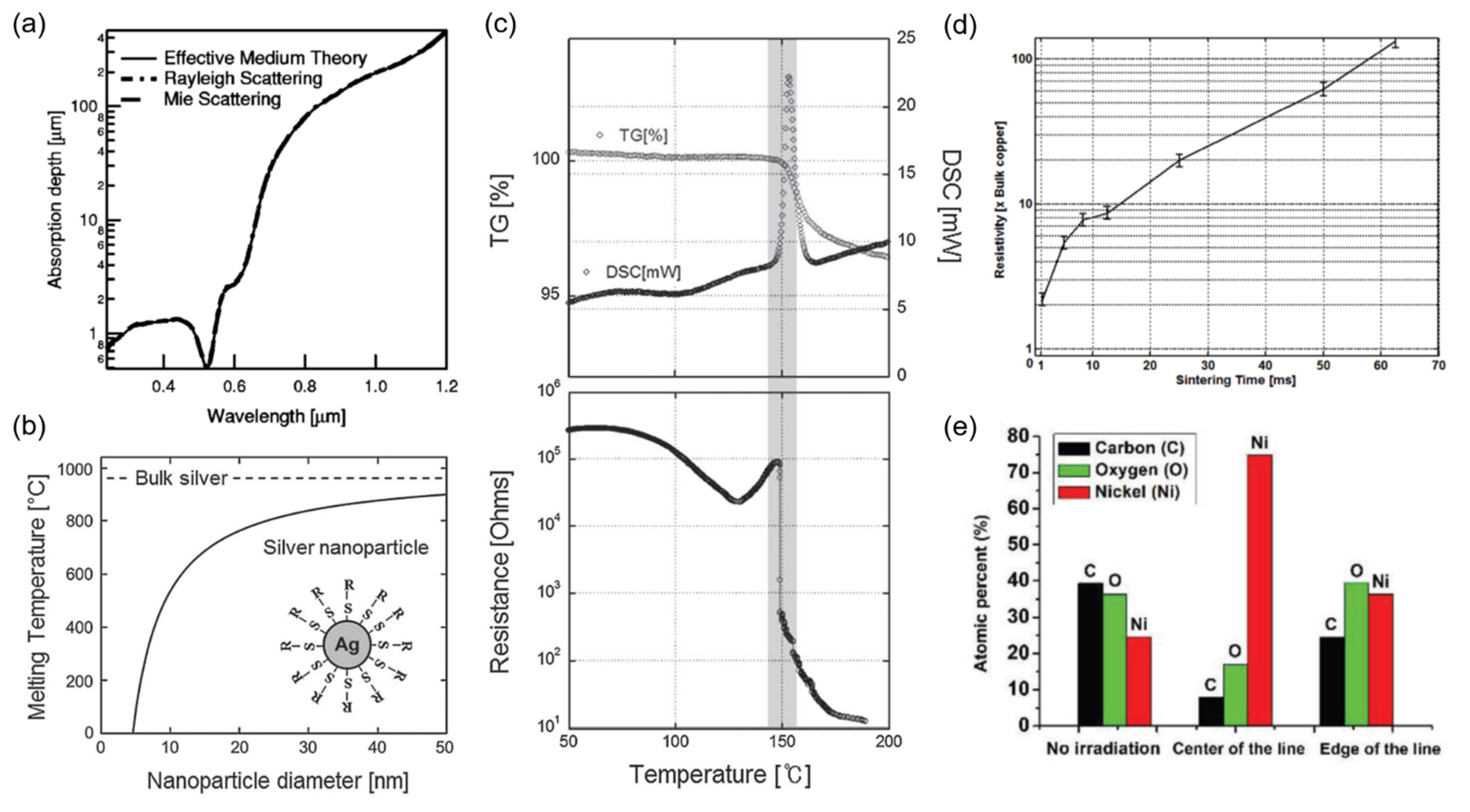
Noble metals, despite their scarcity, have been core materials of interest owing to the excellent stability in ambient conditions and high electrical conductivity. Gold (Au) [17,18,19] has been studied extensively in the early stages in both experimental and theoretical aspects. Absorption depths calculated through different scattering theories [13] suggest that the laser can be utilized as an efficient heating source once the size of the target Au NP is precisely controlled according to laser wavelength. (Figure 1a) Combined with the melting temperature depression phenomenon (Figure 1b), selective laser sintering of Au NP becomes feasible even on heat-sensitive flexible substrates [20]. Analogous ideas have been later applied to different NPs, availing a wide range of materials to laser sintering for flexible and stretchable applications. Early outcomes from laser sintering often show voids at the center of the scanning path [13,21] or an unintended rim [17,22] at the edge due to the thermocapillary force induced by the huge temperature gradient, but such problems can be largely suppressed by controlling solvent evaporation [23]. The excessive thermocapillary force, however, has recently enabled the concept of subtractive laser sintering [24] for highly dense metallic patterns. Molecular dynamic (MD) simulations and experimental studies on lithographically defined Au NPs suggests that the common coalescence time can be in the order of ns after the initial neck growth [25,26,27], yet the characteristic time can be considerably longer given that the number of NP subject to the sintering is much greater in general [28]. The MD simulation also elucidates that other details of the sintering process, which are often difficult to clarify experimentally, e.g., the resultant neck width at different heating rates [26], can be predicted.
As synthesis routes for various silver (Ag) NPs at large quantities have been developed [29], selective laser sintering with Ag NPs has become more common than that of other noble metals [14,30,31]. An Ag NP ink at an average diameter of ~5 nm shows that the melting temperature can be reduced down to ~150 °C as confirmed through thermogravimetric analysis (TGA) and differential scanning calorimeter (DSC) measurements as shown in Figure 1c [14]. Once coupled with low thermal conductivity exhibited by Ag NP compared to its bulk counterpart [32], heat damage can be effectively prevented even on heat-vulnerable substrates [30,33,34] while the resultant electrode exhibits modest robustness against mechanical disturbances [35]. Instead of using presynthesized Ag NP, Ag ion precursor [36,37] or organometallic ink [38] can be employed to achieve laser synthesis and patterning simultaneously. Platinum (Pt), compared to Au and Ag, is not extensively studied [39,40] due to the absence of effective synthesis methods for Pt NP [41]. Recent studies, however, suggest that a Pt layer can be deposited in a precursor liquid environment by laser irradiation to yield outcomes similar to NP sintering [42].
2.2. Copper
Among non-noble metals, copper (Cu) [15,43] receives special attention due to its high electrical conductivity compared to that of noble metals, together with superior cost-effectiveness. A critical issue, however, is that Cu is easily oxidized in ambient conditions. As a result, laser scanning speed, which is directly connected to the local heating time, should be carefully optimized [44,45] along with other laser parameters [46], in order to suppress oxidation. More in-depth experiments have revealed that the effect from oxidation becomes significant once the local heating time exceeds ~1 ms as shown in Figure 1d [15]. For a longer heating time, inert gases such as Nitrogen or Argon [47,48] should be introduced during the sintering process to create a highly conductive metallic layer. At optimum conditions, the properties of the resultant Cu layer surpass those created by thermal annealing [49] as confirmed from XRD and XPS analysis [50]. Instead of reducing the local heating time, acid-assisted laser sintering has been developed [51] to remove the oxide layer, and different types of Cu inks [52] are also under investigation for further improvements.
2.3. Oxides and Others
There are two different approaches for using metal-oxide NPs in the laser sintering technique, either as the oxide material itself or as a precursor for a conductive layer through a reductive sintering process. ZnO and TiO2 are two common oxides that are investigated for sintering processes due to the multiple applications enabled by these materials as functional layers [53,54,55]. Since these oxides possess large band gaps and relatively high melting temperatures, pulsed UV lasers including excimer lasers are widely implemented for efficient sintering, although a CW laser is also a possible option [56]. Upon laser irradiation, the discrete NPs undergo melting and subsequent resolidification steps to change their crystalline structure [53] or phase, which is important for specific applications such as solar cells [54,57]. Direct application of the laser sintering scheme has been also successful with other oxides such as ITO [58], WO3 [59], and more complex oxides [60].
As mentioned, a number of metals suffer from oxidation problems, which become more severe when the material is in NP form that has higher surface-to-volume ratio. Therefore, it is preferable to store an NP in its oxide form and transform it back to its metallic state when needed. A laser-induced photothermochemical reaction enables such reductive sintering of various metal-oxide NPs including CuO [61,62,63,64] and NiO [65,66,67] into their metallic counterparts. (Figure 1e) Through time-resolved normal reflectance measurements, it is suggested that the reductive sintering consists of several steps including densification, reduction and sintering [68]. During the reductive sintering process, slight oxidation can happen at the same time, while a number of intermediate states also can exist [59]. A solvent [61] and capping agent such as polyvinylpyrrolidone (PVP) [16] also play critical role for the corresponding process, acting as both a dispersant and reducing agent.
It should be noted that the range of NPs that is compatible with a laser sintering scheme is continuously growing. Among metals, laser sintering is utilized as a post-process for Al NP slurries to increase the performance of batteries [69]. On the other hand, Zinc (Zn) has been successfully printed and sintered on a bioresorbable polymer substrate through an evaporation–condensation-mediated sintering process [70]. For the improvement of the resultant electrode, nanomaterials with different dimensionality can be mixed with NPs, e.g., Ag nanowire (NW) with Ag NP [71], to create more mechanically robust electrodes, borrowing the idea from steel-wire reinforced concrete. Recent studies include more diverse materials such as liquid metal NP [72], alloy NP [73,74], and coreshell NPs [75] to expand the applications enabled by laser sintering.
3. Experimental Schemes
3.1. Material Deposition
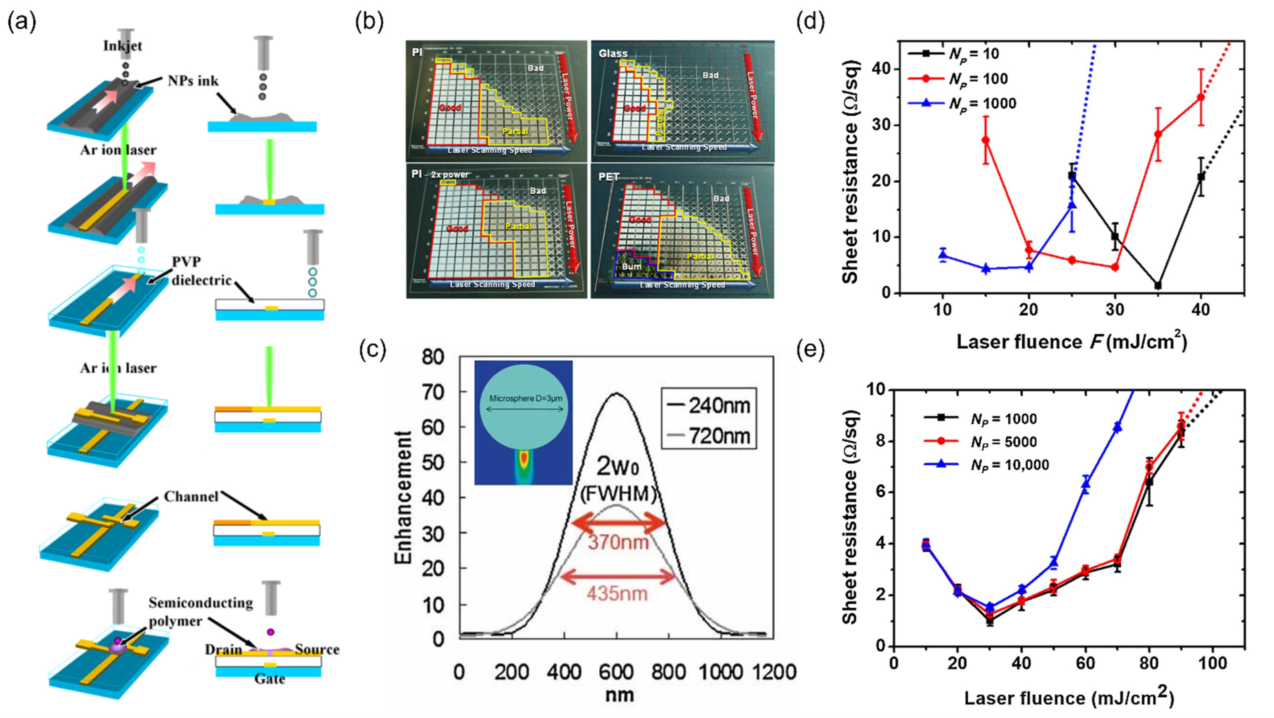
In a typical experiment, a target NP is deposited either uniformly or selectively on the substrate. For uniform deposition of the target NP as a nanoscale thin film, spin-coating is commonly used for a lab-scale experiment [30], however, since the unsintered NPs remain on the substrate, the sample generally undergoes an additional cleaning step after laser irradiation using the solvent of the original NP ink. The unsintered NPs can be recycled after the cleaning step, but for minimum use of the NP from the beginning, the NP is deposited only at the designated position using on-demand printing techniques [18,76] as shown in Figure 2a. The initial feature size immediately after the printing process can be as large as ~100 μm [22], but can be reduced down to several microns by using a tightly focused laser beam as the sintering method [28]. Additional templates such as crack-mediated random networks [77] can be implemented to deposit NP ink partially, but where site-selectivity is not important for the target application, target NPs may be provided by different schemes such as aerosol printing [54,78]. To ensure further scalability of the laser sintering scheme, continuous sintering on roll-to-roll-printed Ag NP has been also demonstrated [79,80].
For specific substrates such as polydimethylsiloxane (PDMS), uniform deposition of NP ink is difficult due to their surface properties, and large differences in the mechanical properties between the substrate and the sintered layer also act as obstacles for efficient processing. As a consequence, different experimental configurations including capillary-assisted [83] and shear-assisted [42,84] laser direct writing have been proposed to overcome such limitation. It is further confirmed that a similar scheme is compatible with a wider polymer substrates [85]. On the other hand, NP can be selectively transferred from the donor substrate to the acceptor substrate using a pulsed laser [86,87,88], which is applicable even to arbitrary 3D structures [89]. It has also been shown recently that ultrafast laser heating enables direct 3D assembly and fusion of nanoparticles to create metallic 3D structure at submicron features through ligand transformation [90].
3.2. Beam Focusing and Scanning Strategies
A laser beam is often focused and scanned at the same time in laser sintering to create an arbitrary pattern with small feature size. The beam spot size created by a focusing lens is directly related to the size of the laser-induced photothermal reaction [91], and the smallest feature size achievable by a high numerical aperture (NA) lens is in the submicron regime [14]. Scanning can be achieved by moving either the sample by a motorized stage [24] or the galvanomirror combined with f-theta telecentric lens [30] which is compatible with continuous production of conductive film by enabling rapid scanning at meters per second [79] (Figure 2b). On the other hand, throughput can be enhanced by creating a number of beamlets using a microlens array (MLA) [92] or a line beam focus using a cylindrical lens [58]. An MLA can be substituted by a self-assembled microsphere array, which also enables submicron feature size by harnessing near-field characteristics as shown in Figure 2c [81]. For an areal pattern, hatch scanning is inevitable with a spherical or a cylindrical lens, yet a digital micromirror device (DMD) can be implemented as an on-demand digital mask to create a designated pattern instantly, analogous to an ‘optical stamp’ [89,93]. Together with the rapid development of laser sources [94], these studies suggest that the laser sintering scheme has strong potential to be a competent processing technique that enables high-resolution patterning over a large area.
3.3. Laser Parameters
Since the physical properties including optical absorbance and thermal characteristics of the target NP are vastly different according to material [95], size [13], and even capping agent [96], selection of adequate laser parameter is a priority [97]. To date, a wide range of lasers at different wavelengths and pulse widths has been successfully implemented as sintering sources, while the details of the resultants may vary. (Figure 2d,e) Since laser sintering is a very complex process that includes a multiphysics problem and various feedbacks between different mechanisms, the optimum laser condition is often found through an experimental parametric study [28,50]. Although it is difficult to understand the exact mechanism behind the sintering process [98], the effects from changing the laser parameters have been investigated in the previous studies. Due to the variation in optical penetration depths, the surface morphologies of the resultant sintered lines as well as the minimum electrical resistivities are different according to the laser wavelength [38,99]. While on the other hand the effect from pulse width is more complex [100]. In terms of processing window, the use of CW laser can be beneficial [101], yet an ultrashort pulsed laser may provide higher conductivity as well as enhanced mechanical properties [82].
4. Applications
Until today, it has been confirmed that the laser sintering process can be applied to a myriad of applications that span from common electronic components to unconventional future-oriented devices. In this review, we focus on three different application categories that have recently achieved notable development by adopting the laser sintering scheme.
4.1. Electrical Interconnections
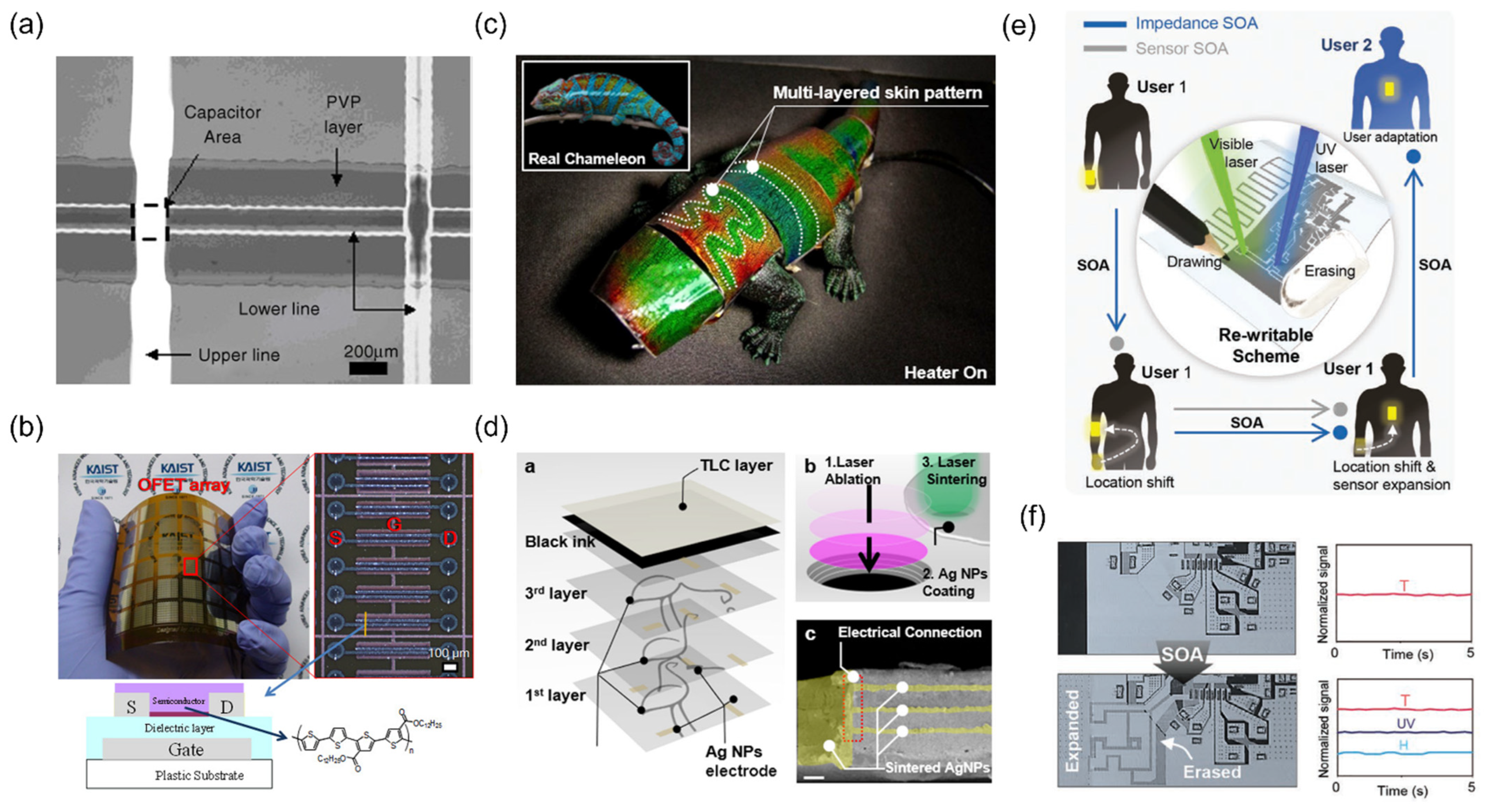
Selective laser sintering is most intensively studied to create a conductive layer, i.e., electrical interconnections on various substrates, which is crucial for both passive and active electronics. As a fine metallic patterns can be immediately created by the selective laser sintering scheme, photolithographically defined conductive lines can be substituted by the laser-sintered conductive lines. For instance, two parallel metallic microlines created on a highly doped silicon wafer can act as the source and the drain of a transistor [18]. Once a semiconductor material such as air-stable carboxylate-functionalized polythiophene is deposited, it is confirmed that the final device with the laser-sintered lines shows similar performance to the one fabricated with lithographical methods. The corresponding discussion, owing to the highly confined heat-affected zone created by the laser sintering process, can be readily extended to multilayer structures even on flexible substrates. When accompanied by laser ablation process that utilizes large difference in ablation thresholds between sintered and unsintered metal NPs, sharply defined multilayer structure is created without any observable damage on the underlying pattern [102]. Multilayer fabrication capability enables the fabrication of other passive electrical components such as a capacitor (Figure 3a) [76], whereas the reliability of the laser-sintered multilayer has further confirmed in the previous study through the production of 11,520 organic field effect transistor (OFET) on 4-inch wafer size flexible substrate as shown in Figure 3b [28].
While on the other hand, we would like to emphasize that the electrical interconnections created by the selective laser sintering have been applied in two novel applications recently. Firstly, laser-sintered metallic electrode is applied to thermochromic liquid crystal (TLC) based artificial chameleon skin (ATACS) [103] to control multiple heaters separately, which is directly associated to the color and the pattern that the device exhibit. The ATACS is composed of a multilayer structure of colorless polyimide (cPI), Ag NW heater and TLC layer (Figure 3c), and the number of layers increases according to the number of target habitats to blend. In previous studies, laser sintering has been applied only to relatively simple multilayer structures, e.g., transistor that requires two distinct layers with metallic electrodes with an insulating layer in between, but the laser sintering can be applied consecutively to realize a more complex multilayer structure. In this regard, the laser sintering steps are repeated more than three times for the fabrication of ATACS, accompanied by laser ablation process to create via holes, to enable complete electrical interconnections for the final multilayer structure as shown in Figure 3d. The resultant ATACS not only shows clear patterns according to the activation of each heater, but also superior stability towards mechanical disturbances.
Secondly, laser-sintered metallic electrode enables a new concept of evolvable skin electronics, of which system’s impedance and functions can be altered during the operation [104]. The objective of a wearable electronics can be diverse, yet the one of the primary concerns is to measure various physiological data from the body to acquire the current state of the wearer, especially for healthcare purpose. Given that only a single device is used, the conventional wearable device can face the following problems: necessity of new functionality and mismatch of system impedance once the system is altered. The research demonstrates that the combination of laser sintering and ablation of metallic NP using CW laser and pulsed laser (Figure 3e) enables in-situ and in-operando adaptation (SOA) for active, customized wearable devices. By connecting new electronic element via laser sintering, additional measurements, e.g., UV and humidity sensors, become available for the original device (Figure 3f), and it is also confirmed that the system impedance can be optimized according to the body parts, e.g., hand, wrist, chest, where the device is attached. These reports present that the laser sintering scheme is now at a mature technological level and compatible to a complex multilayer structure, while more advanced device concept is realizable, e.g., reprogrammability, once it is combined with other supplementary processes.
4.2. Sensors
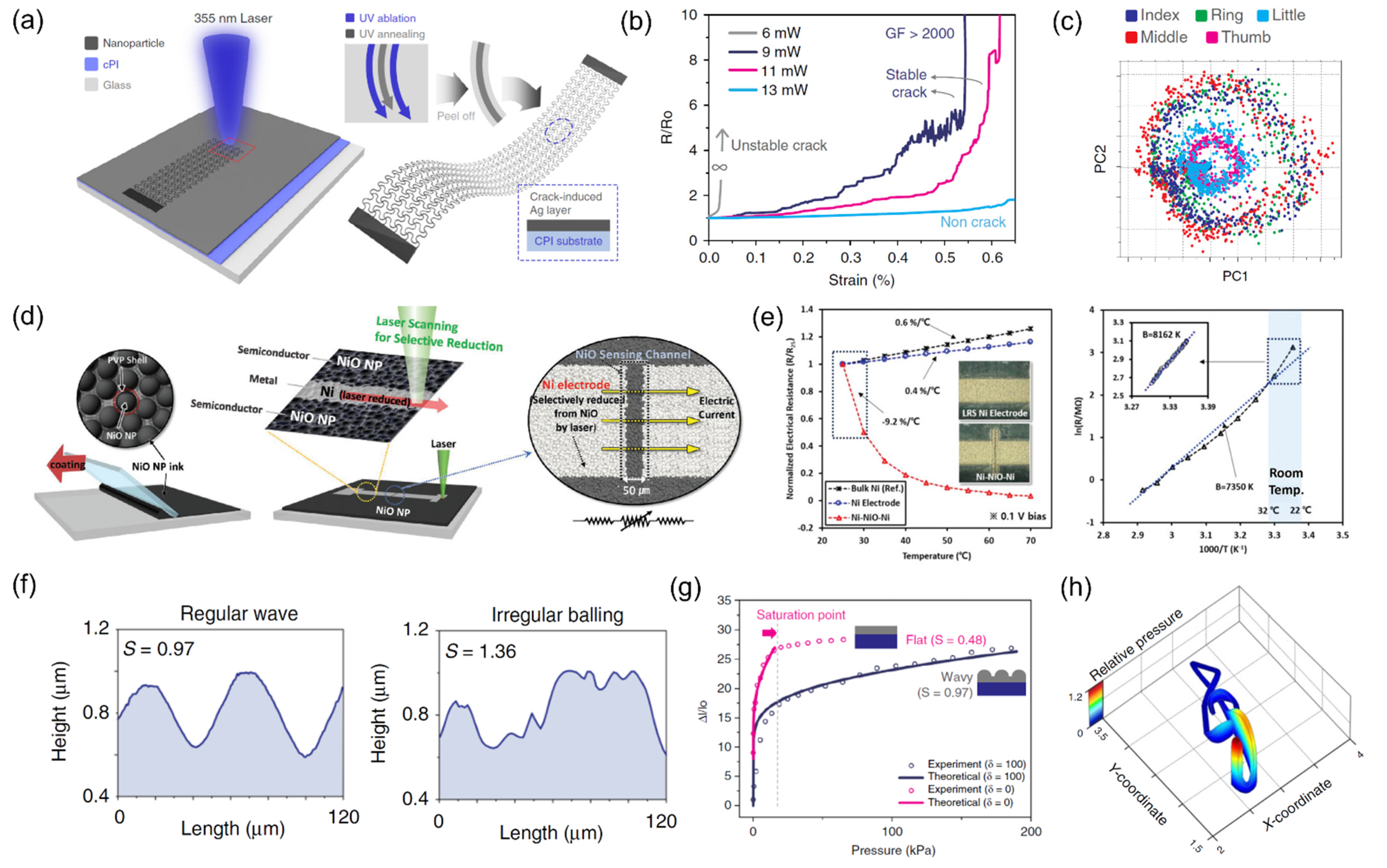
Among diverse sensors, a strain-gauge is often the simplest sensor that consists of metallic strips of known electrical properties under the applied strain. Similar to the aforementioned electrical interconnections, the strain-dependent metallic strip can be directly substituted by the laser-sintered metallic layers [105]. The laser-printed metallic strain gauge responses well to the applied stretch or deflection [70] which is predictable from any other strain sensor. Recent skin sensor demonstrated by Kim et al. [106], on the other hand, proves that the laser sintering possesses great potential to be an efficient manufacturing technique for a next-generation motion sensor that has not been reported before. In this study, Ag NP coated cPI is exposed to UV pulsed laser to complete two different tasks: ablation of cPI and sintering of Ag NP. The resultant is composed of underlying serpentine structure and a crack-induced Ag NP layer. (Figure 4a) The serpentine structure ensures a conformal contact of the sensor with the epidermis accompanied with high stability towards the overall strain, while the cracked layer acts as a highly sensitive strain sensor whose gauge factor can be as large as 2000 (Figure 4b) comparable to other crack-based sensors [107]. Due to its high sensitivity and excellent conformality to the skin, the laser-produced sensor captures previously undetectable signals, which can be decoded to classify various human movements. In particular, the device successfully distinguishes five motions from each finger by attaching a single sensor at the wrist by the aid of a deep neural network, potentiating that the number of sensors required to detect the human motion can be reduced greatly by the simultaneous use of ultrasensitive sensor and machine learning scheme (Figure 4c).
Along with the interests in human-attached sensors to obtain the motion of the wearer, the acquisition of physiological sensor is gaining rapid attention as well due to the rise in the importance of remote healthcare devices for an upcoming aging society. Similar to the discussion above, a change in certain physiological data can be monitored once the physical properties of the sensor are known in advance, but the sensitivity of the sensor is often a problem: a very subtle changes, e.g., temperature variation from exhalation and inhalation of human breathing [108], are often undetectable due to the limited sensitivity. In this regard, Shin et al. proposed an interesting approach to create an ultrasensitive temperature sensor on a flexible substrate monolithically based on the reductive laser sintering scheme [109]. In a typical reductive sintering process, metal oxide nanoparticle is transformed into a continuous metallic layer by scanning the focused laser line by line at a fixed hatch distance. In their study, several scanning lines are skipped intentionally to leave a thin native oxide layer (Figure 4d). The remaining oxide layer, which is NiO in their study, acts as a transition metal oxide channel that shows the characteristics of negative temperature coefficient (NTC) thermistor within the resultant Ni-NiO-Ni heterostructure. Interestingly, the TCR of the resultant temperature sensor is measured to be −9.2%/°C, which yields an extremely high B-value of 8162 K (Figure 4e). It is suggested that such high sensitivity is closely related to various vacancies introduced by the confined photothermal heating.
A touch screen panel is another sensing element that has drawn great attention since the last decade due to rapid increase in the use of portable devices that requires a human–machine interface including mobile phones and tablet PCs. A transparent conductor is a crucial component for the creation of the touch screen panel either for a resistive [30] or a capacitive [111] type, and laser sintering of metal nanoparticle provides an efficient substitute to the conventional ITO-based transparent conductor by forming a regular [30] or a quasi-random [112] metallic grid that is practically invisible to bare human eye. From such simple replacement, huge advancement has been achieved by the recent work by Kim et al. [110]. In their study, the researchers focus on the spontaneous balling effect created upon the laser sintering process, which is often regarded as a metallurgical defect that should be avoided. At a certain laser condition, it is confirmed that regular corrugated structure can be formed (Figure 4f) once the speed of the laser-induced circulating Marangoni flow matches the solidification rate, denoted as a dimensionless number called the surface shaping number. By having well-defined, multiscale metallic structure, the contact area and therefore the electrical pathway changes upon the application of pressure (Figure 4g), which is analyzed to enable the acquisition of pressure information while reading the lateral position as well (Figure 4h).
4.3. Heaters
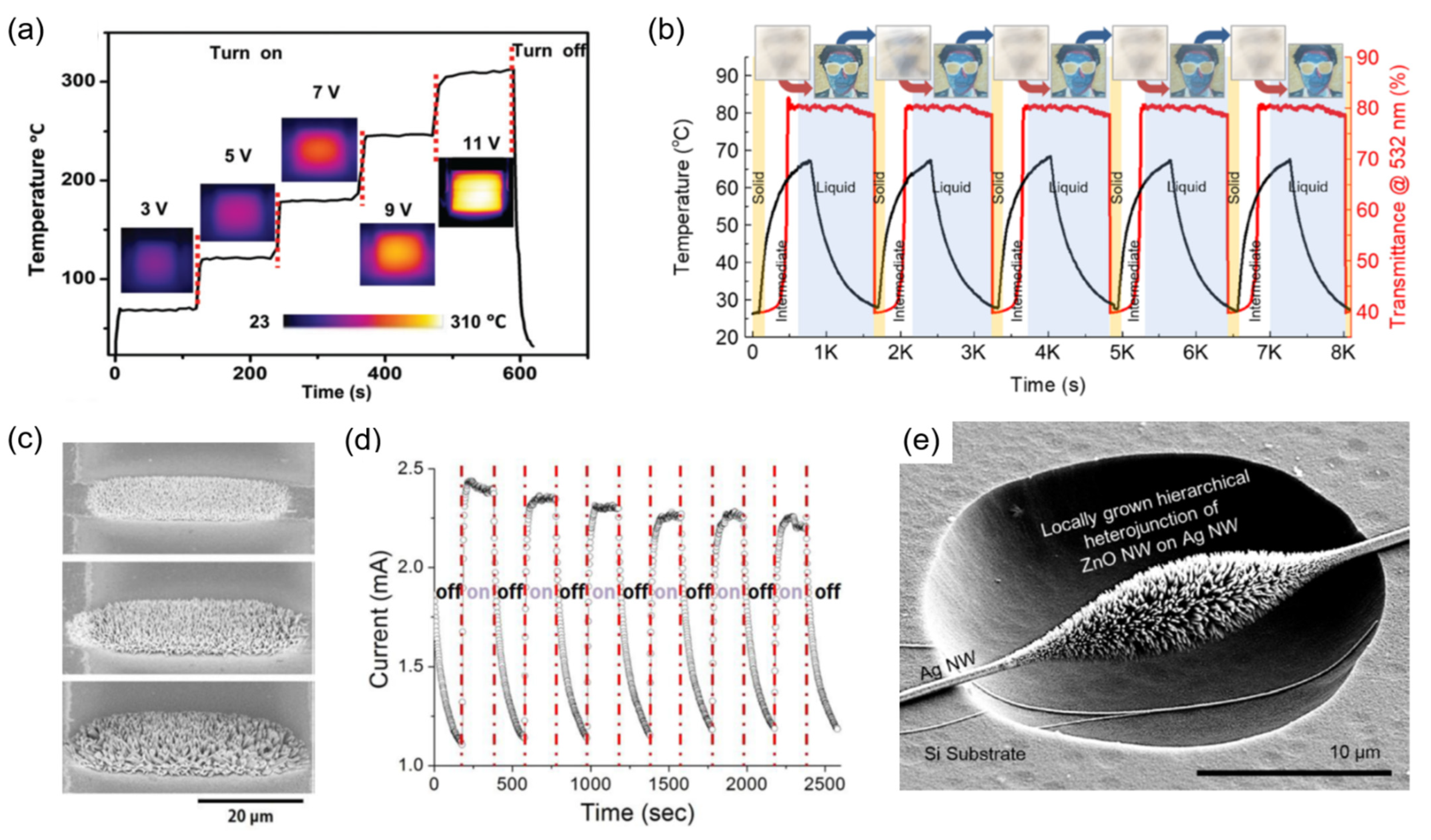
A heater based on the resistive Joule heating is a component that typically operates under a harsh condition. As a consequence, the robustness of the heater including the stability of the heating electrode at high current and its adhesion to the substrate becomes more important compared to other applications. The laser-sintered metallic layer has been studied extensively especially in the form of a transparent heater [51,112], and special attention has been made to the ones based on a laser-sintered Ni electrode [113] due to its superior thermal stability compared to other non-noble metals. In particular, Nam et al. creates a transparent Ni-based heater on cPI substrate to realize a flexible and transparent heater that aims for high temperature applications. Owing to the outstanding thermal stabilities of both electrode (Ni) and substrate (cPI), the resultant heater operates constantly up to 310 °C while exhibiting rapid heating and cooling characteristics together with excellent mechanical properties. (Figure 5a) As the heaters based on the laser-sintered electrodes become more reliable, they are increasingly applied to proof-of-concept devices such as the recent mechano-thermo-chromic (MTC) device [114] that requires rapid prototyping (Figure 5b).
A more common demonstration coupled to the laser-sintered heater is defrosting or defogging [112], yet the resultant laser-sintered heaters can withstand direct contact to the liquid surrounding. In this regard, the heater based on the laser-sintered electrode has been further applied as the heating source to induce hydrothermal growth at the corresponding electrode to create heterogeneous nanostructure, especially aimed for the synthesis of functional metal-oxide NWs. These attempts can be classified into two categories: in the first, NWs are directly synthesized hydrothermally on the laser-sintered electrode acting as a heating source [115]. It is demonstrated that dense Zinc Oxide (ZnO) NW can be synthesized locally on the laser-sintered electrodes by utilizing them as microscopic heaters (Figure 5c). These NWs expand the functionality of the electrode as shown in the demonstration of a UV sensor composed of two adjacent laser-sintered electrodes which are connected by the hydrothermally synthesized ZnO NW arrays (Figure 5d). On the other hand, laser sintering can be employed to capture another conductive NW, e.g., Ag NW, since the entire sintering process can be easily monitored and controlled at high precision. The captured Ag NW then acts as the template for secondary growth by the aid of electrothermal [117] or photothermal [116] heating (Figure 5e). Through this scheme, the area subject to the NW growth can be reduced down to sub-diffraction regime to enable nanoscale devices.
5. Conclusions and Perspective
Selective laser sintering of functional nanoparticles, which has been actively studied in the last two decades, has opened a new route towards facile creation of functional layers. As summarized in this review, major advances have been achieved in every aspect. Starting from noble metals, wide ranges of materials including non-noble metals, metal-oxides and even alloys are now compatible with the laser sintering scheme, enabling the creation of not only simple electrical connections but also active components in ambient condition for more sophisticated, smart devices. The minimum feature size can be reduced even beyond the diffraction limit, whereas continuous efforts are made to increase the overall production throughput by scrutinizing diverse optical schemes, assisted by rapid development in high power laser sources. The laser sintering scheme was first started as a facile substitution for other conventional fabrication techniques, but a number of recent studies reveal that unique morphological and physical characteristics of the resultant often enable rather unexpected breakthroughs to the existing concepts as representatively shown in the examples of the 3D touch screen sensor and the ultrasensitive temperature sensor.
Along with active use of the laser sintering scheme, we predict several future development directions regarding the relevant emerging applications. First, a selective laser process is actively investigated for efficient utilization of other nanomaterials as well, including NWs and 2D materials in particular [118]. A laser is proven to be a useful tool for direct and facile processing of these materials, and a wide range of techniques have been developed, e.g., positioning [119,120], ablation [111], nano-welding [121], pyrolysis [122], modification [123], thinning [124], etc. As a result, the materials which are in the spotlight for next-generation applications are largely compatible with laser processes. Recent studies on the laser process of PI and PDMS, which are common substrates for flexible/stretchable electronics and healthcare devices, further confirm that high-quality micromachining [7,125] as well as adhesive-free bonding [126] between these two substrates are realizable through the laser-induced photothermal reaction. These developmental aspects suggest that laser processes can be among the core fabrication technique for emerging applications, heading towards all-laser fabrication of a device [127,128] up to a system level. We also expect that the laser process will become more valuable as the global semiconductor shortage continues.
Selective laser sintering of nanoparticles can be regarded as a laser additive manufacturing technique, an area that has seen major advancements over the past few years [129,130,131]. As a consequence, the research trends as well as scientific challenges and issues are analogous. Major advantages of additive manufacturing are flexible design and rapid prototyping, and as a result, mechanical metamaterials such as auxetic structures with a negative Poisson ratio [132,133,134,135,136,137,138,139,140,141] can be readily produced and tested by the corresponding technique. Laser-assisted sintering is a highly non-equilibrium process that incorporates a very complicated multiphysics problem with various feedbacks. As a result, in-situ sensing and monitoring of the laser-assisted process [142] are currently subjects of active study, especially to recognize different types of defects in real time. Data-driven optimization of selective laser sintering, e.g., the deep learning approach for tool paths [143], is also becoming popular, and we expect that similar approaches will be investigated for the industrialization of laser sintering processes for nanoparticles.
Author Contributions
Conceptualization, S.H.; investigation, E.H. and J.H.; writing—original draft preparation, E.H.; writing—review and editing, S.H.; visualization, J.H.; supervision, J.Y. and S.H.; project administration, S.H.; funding acquisition, J.Y. and S.H. All authors have read and agreed to the published version of the manuscript.
Funding
This work was supported by the Basic Research Program through the National Research Foundation of Korea (NRF) funded by the MSIT (grant number: 2022R1A4A3031263). Also, this work was supported by the research fund of Hanyang University (HY-2020-2470).
Institutional Review Board Statement
Not applicable.
Informed Consent Statement
Not applicable.
Data Availability Statement
Data sharing is not applicable.
Acknowledgments
E.H. acknowledges a fellowship from the Hyundai Motor Chung Mong-Koo Foundation.
Conflicts of Interest
The authors declare no conflict of interest.
References
- Kim, H.; Pyun, K.R.; Lee, M.T.; Lee, H.B.; Ko, S.H. Recent Advances in Sustainable Wearable Energy Devices with Nanoscale Materials and Macroscale Structures. Adv. Funct. Mater. 2022, 32, 2110535. [Google Scholar] [CrossRef]
- Kim, K.K.; Choi, J.; Ko, S.H. Energy harvesting untethered soft electronic devices. Adv. Healthc. Mater. 2021, 10, 2002286. [Google Scholar] [CrossRef]
- Won, P.; Kim, K.K.; Kim, H.; Park, J.J.; Ha, I.; Shin, J.; Jung, J.; Cho, H.; Kwon, J.; Lee, H. Transparent soft actuators/sensors and camouflage skins for imperceptible soft robotics. Adv. Mater. 2021, 33, 2002397. [Google Scholar] [CrossRef] [PubMed]
- Huang, Q.; Zhu, Y. Printing conductive nanomaterials for flexible and stretchable electronics: A review of materials, processes, and applications. Adv. Mater. Technol. 2019, 4, 1800546. [Google Scholar] [CrossRef]
- Jung, D.; Lim, C.; Shim, H.J.; Kim, Y.; Park, C.; Jung, J.; Han, S.I.; Sunwoo, S.-H.; Cho, K.W.; Cha, G.D. Highly conductive and elastic nanomembrane for skin electronics. Science 2021, 373, 1022–1026. [Google Scholar] [CrossRef]
- May, G.S.; Spanos, C.J. Fundamentals of Semiconductor Manufacturing and Process Control; John Wiley & Sons: Hoboken, NJ, USA, 2006. [Google Scholar]
- Shin, J.; Ko, J.; Jeong, S.; Won, P.; Lee, Y.; Kim, J.; Hong, S.; Jeon, N.L.; Ko, S.H. Monolithic digital patterning of polydimethylsiloxane with successive laser pyrolysis. Nat. Mater. 2021, 20, 100–107. [Google Scholar] [CrossRef] [PubMed]
- Shishkovsky, I. Sintering of Functional Materials; BoD–Books on Demand: Norderstedt, Germany, 2018. [Google Scholar]
- Buffat, P.; Borel, J.P. Size effect on the melting temperature of gold particles. Phys. Rev. A 1976, 13, 2287. [Google Scholar] [CrossRef]
- Huang, X.; El-Sayed, M.A. Gold nanoparticles: Optical properties and implementations in cancer diagnosis and photothermal therapy. J. Adv. Res. 2010, 1, 13–28. [Google Scholar] [CrossRef]
- Heiligtag, F.J.; Niederberger, M. The fascinating world of nanoparticle research. Mater. Today 2013, 16, 262–271. [Google Scholar] [CrossRef]
- Khan, I.; Saeed, K.; Khan, I. Nanoparticles: Properties, applications and toxicities. Arab. J. Chem. 2019, 12, 908–931. [Google Scholar] [CrossRef]
- Bieri, N.R.; Chung, J.; Haferl, S.E.; Poulikakos, D.; Grigoropoulos, C.P. Microstructuring by printing and laser curing of nanoparticle solutions. Appl. Phys. Lett. 2003, 82, 3529–3531. [Google Scholar] [CrossRef]
- Son, Y.; Yeo, J.; Moon, H.; Lim, T.W.; Hong, S.; Nam, K.H.; Yoo, S.; Grigoropoulos, C.P.; Yang, D.-Y.; Ko, S.H. Nanoscale Electronics: Digital Fabrication by Direct Femtosecond Laser Processing of Metal Nanoparticles. Adv. Mater. 2011, 23, 3176–3181. [Google Scholar] [CrossRef] [PubMed]
- Zenou, M.; Ermak, O.; Saar, A.; Kotler, Z. Laser sintering of copper nanoparticles. J. Phys. D Appl. Phys. 2013, 47, 025501. [Google Scholar] [CrossRef]
- Nam, V.B.; Shin, J.; Yoon, Y.; Giang, T.T.; Kwon, J.; Suh, Y.D.; Yeo, J.; Hong, S.; Ko, S.H.; Lee, D. Highly Stable Ni-Based Flexible Transparent Conducting Panels Fabricated by Laser Digital Patterning. Adv. Funct. Mater. 2019, 29, 1806895. [Google Scholar] [CrossRef]
- Chung, J.; Ko, S.; Bieri, N.R.; Grigoropoulos, C.P.; Poulikakos, D. Conductor microstructures by laser curing of printed gold nanoparticle ink. Appl. Phys. Lett. 2004, 84, 801–803. [Google Scholar] [CrossRef]
- Ko, S.H.; Pan, H.; Grigoropoulos, C.P.; Luscombe, C.K.; Fréchet, J.M.J.; Poulikakos, D. Air stable high resolution organic transistors by selective laser sintering of ink-jet printed metal nanoparticles. Appl. Phys. Lett. 2007, 90, 141103. [Google Scholar] [CrossRef]
- Yamaguchi, M.; Araga, S.; Mita, M.; Yamasaki, K.; Maekawa, K. On-demand infrared laser sintering of gold nanoparticle paste for electrical contacts. IEEE Trans. Compon. Packag. Manuf. Technol. 2015, 5, 1160–1168. [Google Scholar] [CrossRef]
- Ko, S.H.; Pan, H.; Grigoropoulos, C.P.; Luscombe, C.K.; Fréchet, J.M.J.; Poulikakos, D. All-inkjet-printed flexible electronics fabrication on a polymer substrate by low-temperature high-resolution selective laser sintering of metal nanoparticles. Nanotechnology 2007, 18, 345202. [Google Scholar] [CrossRef]
- Lim, J.; Ham, J.; Lee, W.; Hwang, E.; Lee, W.C.; Hong, S. A Transformative Gold Patterning through Selective Laser Refining of Cyanide. Nanomaterials 2021, 11, 1921. [Google Scholar] [CrossRef]
- Chung, J.; Bieri, N.R.; Ko, S.; Grigoropoulos, C.P.; Poulikakos, D. In-tandem deposition and sintering of printed gold nanoparticle inks induced by continuous Gaussian laser irradiation. Appl. Phys. A 2004, 79, 1259–1261. [Google Scholar] [CrossRef]
- Chung, J.; Ko, S.; Grigoropoulos, C.P.; Bieri, N.R.; Dockendorf, C.; Poulikakos, D. Damage-Free Low Temperature Pulsed Laser Printing of Gold Nanoinks On Polymers. J. Heat Transf. 2005, 127, 724–732. [Google Scholar] [CrossRef]
- Park, S.; Kwon, J.; Lim, J.; Shin, W.; Lee, Y.; Lee, H.; Kim, H.-J.; Han, S.; Yeo, J.; Ko, S.H. Micropatterning of metal nanoparticle ink by laser-induced thermocapillary flow. Nanomaterials 2018, 8, 645. [Google Scholar] [CrossRef] [PubMed]
- Pan, H.; Ko, S.H.; Grigoropoulos, C.P. The Solid-State Neck Growth Mechanisms in Low Energy Laser Sintering of Gold Nanoparticles: A Molecular Dynamics Simulation Study. J. Heat Transf. 2008, 130, 092404. [Google Scholar] [CrossRef]
- Yang, L.; Gan, Y.; Zhang, Y.; Chen, J.K. Molecular dynamics simulation of neck growth in laser sintering of different-sized gold nanoparticles under different heating rates. Appl. Phys. A 2012, 106, 725–735. [Google Scholar] [CrossRef]
- Pan, H.; Ko, S.H.; Grigoropoulos, C.P. The coalescence of supported gold nanoparticles induced by nanosecond laser irradiation. Appl. Phys. A 2008, 90, 247–253. [Google Scholar] [CrossRef]
- Yeo, J.; Hong, S.; Lee, D.; Hotz, N.; Lee, M.-T.; Grigoropoulos, C.P.; Ko, S.H. Next Generation Non-Vacuum, Maskless, Low Temperature Nanoparticle Ink Laser Digital Direct Metal Patterning for a Large Area Flexible Electronics. PLoS ONE 2012, 7, e42315. [Google Scholar] [CrossRef]
- Wani, I.A.; Khatoon, S.; Ganguly, A.; Ahmed, J.; Ganguli, A.K.; Ahmad, T. Silver nanoparticles: Large scale solvothermal synthesis and optical properties. Mater. Res. Bull. 2010, 45, 1033–1038. [Google Scholar] [CrossRef]
- Hong, S.; Yeo, J.; Kim, G.; Kim, D.; Lee, H.; Kwon, J.; Lee, H.; Lee, P.; Ko, S.H. Nonvacuum, Maskless Fabrication of a Flexible Metal Grid Transparent Conductor by Low-Temperature Selective Laser Sintering of Nanoparticle Ink. ACS Nano 2013, 7, 5024–5031. [Google Scholar] [CrossRef]
- Kurnoothala, R.; Vishnubhatla, K.C. Facile fabrication of integrated microfluidic SERS substrate by femtosecond laser sintering of silver nano particles. Opt. Mater. 2021, 111, 110518. [Google Scholar] [CrossRef]
- Son, Y.; Yeo, J.; Ha, C.W.; Lee, J.; Hong, S.; Nam, K.H.; Yang, D.-Y.; Ko, S.H. Application of the specific thermal properties of Ag nanoparticles to high-resolution metal patterning. Thermochim. Acta 2012, 542, 52–56. [Google Scholar] [CrossRef]
- Yang, Y.; Li, Z.; Yang, S.; Li, Y.; Huang, J. Multiscale simulation study of laser sintering of inkjet-printed silver nanoparticle inks. Int. J. Heat Mass Transf. 2020, 159, 120110. [Google Scholar] [CrossRef]
- Ko, S.H.; Pan, H.; Ryu, S.G.; Misra, N.; Grigoropoulos, C.P.; Park, H.K. Nanomaterial enabled laser transfer for organic light emitting material direct writing. Appl. Phys. Lett. 2008, 93, 151110. [Google Scholar] [CrossRef]
- Yang, M.; Chon, M.-W.; Kim, J.-H.; Lee, S.-H.; Jo, J.; Yeo, J.; Ko, S.H.; Choa, S.-H. Mechanical and environmental durability of roll-to-roll printed silver nanoparticle film using a rapid laser annealing process for flexible electronics. Microelectron. Reliab. 2014, 54, 2871–2880. [Google Scholar] [CrossRef]
- Liu, Y.-K.; Lee, M.-T. Laser Direct Synthesis and Patterning of Silver Nano/Microstructures on a Polymer Substrate. ACS Appl. Mater. Interfaces 2014, 6, 14576–14582. [Google Scholar] [CrossRef] [PubMed]
- Tsai, S.-L.; Liu, Y.-K.; Pan, H.; Liu, C.-H.; Lee, M.-T. The coupled photothermal reaction and transport in a laser additive metal nanolayer simultaneous synthesis and pattering for flexible electronics. Nanomaterials 2016, 6, 12. [Google Scholar] [CrossRef]
- Kang, B.; Ko, S.; Kim, J.; Yang, M. Microelectrode fabrication by laser direct curing of tiny nanoparticle self-generated from organometallic ink. Opt. Express 2011, 19, 2573–2579. [Google Scholar] [CrossRef] [PubMed]
- Cai, Z.X.; Zeng, X.Y.; Duan, J. Fabrication of platinum microheater on alumina substrate by micro-pen and laser sintering. Thin Solid Film. 2011, 519, 3893–3896. [Google Scholar] [CrossRef]
- Kang, T.Y.; Yoo, K.; Lee, J.A.; Lee, W.; Kim, K.; Lee, D.-K.; Kim, H.; Ko, M.J. A facile and rapid process to fabricate platinum counter electrode in dye-sensitized solar cell using nanosecond pulsed laser sintering at room temperature. J. Nanosci. Nanotechnol. 2014, 14, 5309–5312. [Google Scholar] [CrossRef] [PubMed]
- Tsuji, T.; Suzuki, Y.; Sakaki, S.; Ishikawa, Y.; Koshizaki, N. Preparation of binder-free spherical submicron-sized platinum particles using laser melting in liquids. Electron. Commun. Jpn. 2021, 104, e12330. [Google Scholar] [CrossRef]
- Edri, E.; Armon, N.; Greenberg, E.; Moshe-Tsurel, S.; Lubotzky, D.; Salzillo, T.; Perelshtein, I.; Tkachev, M.; Girshevitz, O.; Shpaisman, H. Laser printing of multilayered alternately conducting and insulating microstructures. ACS Appl. Mater. Interfaces 2021, 13, 36416–36425. [Google Scholar] [CrossRef]
- Hayati-Roodbari, N.; Wheeldon, A.; Hendler, C.; Fian, A.; Trattnig, R. Ohmic contact formation for inkjet-printed nanoparticle copper inks on highly doped GaAs. Nanotechnology 2021, 32, 225205. [Google Scholar] [CrossRef] [PubMed]
- Halonen, E.; Heinonen, E.; Mäntysalo, M. The Effect of Laser Sintering Process Parameters on Cu Nanoparticle Ink in Room Conditions. Opt. Photonics J. 2013, 3, 5. [Google Scholar] [CrossRef]
- Soltani, A.; Vahed, B.K.; Mardoukhi, A.; Mäntysalo, M. Laser sintering of copper nanoparticles on top of silicon substrates. Nanotechnology 2015, 27, 035203. [Google Scholar] [CrossRef]
- Yang, G.; Xu, G.; Li, Q.; Zeng, Y.; Zhang, Y.; Hao, M.; Cui, C. Understanding the sintering and heat dissipation behaviours of Cu nanoparticles during low-temperature selective laser sintering process on flexible substrates. J. Phys. D Appl. Phys. 2021, 54, 375304. [Google Scholar] [CrossRef]
- Joo, M.; Lee, B.; Jeong, S.; Lee, M. Laser sintering of Cu paste film printed on polyimide substrate. Appl. Surf. Sci. 2011, 258, 521–524. [Google Scholar] [CrossRef]
- Joo, M.; Lee, B.; Jeong, S.; Lee, M. Comparative studies on thermal and laser sintering for highly conductive Cu films printable on plastic substrate. Thin Solid Film. 2012, 520, 2878–2883. [Google Scholar] [CrossRef]
- Yu, J.H.; Kang, K.-T.; Hwang, J.Y.; Lee, S.-H.; Kang, H. Rapid sintering of copper nano ink using a laser in air. Int. J. Precis. Eng. Manuf. 2014, 15, 1051–1054. [Google Scholar] [CrossRef]
- Kwon, J.; Cho, H.; Eom, H.; Lee, H.; Suh, Y.D.; Moon, H.; Shin, J.; Hong, S.; Ko, S.H. Low-temperature oxidation-free selective laser sintering of Cu nanoparticle paste on a polymer substrate for the flexible touch panel applications. ACS Appl. Mater. Interfaces 2016, 8, 11575–11582. [Google Scholar] [CrossRef]
- Kwon, J.; Cho, H.; Suh, Y.D.; Lee, J.; Lee, H.; Jung, J.; Kim, D.; Lee, D.; Hong, S.; Ko, S.H. Flexible and transparent cu electronics by low-temperature acid-assisted laser processing of Cu nanoparticles. Adv. Mater. Technol. 2017, 2, 1600222. [Google Scholar] [CrossRef]
- Min, H.; Lee, B.; Jeong, S.; Lee, M. Fabrication of 10 µm-scale conductive Cu patterns by selective laser sintering of Cu complex ink. Opt. Laser Technol. 2017, 88, 128–133. [Google Scholar] [CrossRef]
- Pan, H.; Misra, N.; Ko, S.H.; Grigoropoulos, C.P.; Miller, N.; Haller, E.E.; Dubon, O. Melt-mediated coalescence of solution-deposited ZnO nanoparticles by excimer laser annealing for thin-film transistor fabrication. Appl. Phys. A 2009, 94, 111–115. [Google Scholar] [CrossRef]
- Pan, H.; Ko, S.H.; Misra, N.; Grigoropoulos, C.P. Laser annealed composite titanium dioxide electrodes for dye-sensitized solar cells on glass and plastics. Appl. Phys. Lett. 2009, 94, 071117. [Google Scholar] [CrossRef]
- Lee, D.; Pan, H.; Ko, S.H.; Park, H.K.; Kim, E.; Grigoropoulos, C.P. Non-vacuum, single-step conductive transparent ZnO patterning by ultra-short pulsed laser annealing of solution-deposited nanoparticles. Appl. Phys. A 2012, 107, 161–171. [Google Scholar] [CrossRef]
- Sandmann, A.; Notthoff, C.; Winterer, M. Continuous wave ultraviolet-laser sintering of ZnO and TiO2 nanoparticle thin films at low laser powers. J. Appl. Phys. 2013, 113, 044310. [Google Scholar] [CrossRef]
- Ming, L.; Yang, H.; Zhang, W.; Zeng, X.; Xiong, D.; Xu, Z.; Wang, H.; Chen, W.; Xu, X.; Wang, M. Selective laser sintering of TiO2 nanoparticle film on plastic conductive substrate for highly efficient flexible dye-sensitized solar cell application. J. Mater. Chem. A 2014, 2, 4566–4573. [Google Scholar] [CrossRef]
- Pan, H.; Lee, D.; Ko, S.H.; Grigoropoulos, C.P.; Park, H.K.; Hoult, T. Fiber laser annealing of indium-tin-oxide nanoparticles for large area transparent conductive layers and optical film characterization. Appl. Phys. A 2011, 104, 29–38. [Google Scholar] [CrossRef]
- Cho, H.; Min, J.; Won, D.; Kwon, J.; Ko, S.H. Selective photo-thermal conversion of tungsten oxide sol precursor for electrochromic smart window applications. Acta Mater. 2020, 201, 528–534. [Google Scholar] [CrossRef]
- Wang, J.; Lisco, F.; Hutt, D.A.; Jones, L.C.; Bowers, J.W.; Isherwood, P.J.; Zhou, Z.; Conway, P.P. Laser sintering and patterning of gallium-doped zinc oxide/indium-tin oxide nanoparticle films with tailorable electrical and optical properties. Mater. Des. 2020, 194, 108865. [Google Scholar] [CrossRef]
- Kang, B.; Han, S.; Kim, J.; Ko, S.; Yang, M. One-Step Fabrication of Copper Electrode by Laser-Induced Direct Local Reduction and Agglomeration of Copper Oxide Nanoparticle. J. Phys. Chem. C 2011, 115, 23664–23670. [Google Scholar] [CrossRef]
- Rahman, M.K.; Lu, Z.; Kwon, K.-S. Green laser sintering of copper oxide (CuO) nano particle (NP) film to form Cu conductive lines. AIP Adv. 2018, 8, 095008. [Google Scholar] [CrossRef] [Green Version]
- Nam, V.B.; Giang, T.T.; Lee, D. Laser digital patterning of finely-structured flexible copper electrodes using copper oxide nanoparticle ink produced by a scalable synthesis method. Appl. Surf. Sci. 2021, 570, 151179. [Google Scholar]
- Liu, H.; Liu, Y.; Guo, W.; Zhou, X.; Lin, L.; Peng, P. Laser assisted ink-printing of copper oxide nanoplates for memory device. Mater. Lett. 2020, 261, 127097. [Google Scholar] [CrossRef]
- Lee, D.; Paeng, D.; Park, H.K.; Grigoropoulos, C.P. Vacuum-Free, Maskless Patterning of Ni Electrodes by Laser Reductive Sintering of NiO Nanoparticle Ink and Its Application to Transparent Conductors. ACS Nano 2014, 8, 9807–9814. [Google Scholar] [CrossRef] [PubMed]
- Rho, Y.; Kang, K.-T.; Lee, D. Highly crystalline Ni/NiO hybrid electrodes processed by inkjet printing and laser-induced reductive sintering under ambient conditions. Nanoscale 2016, 8, 8976–8985. [Google Scholar] [CrossRef] [PubMed]
- Nam, V.B.; Lee, D. Evaluation of Ni-based flexible resistance temperature detectors fabricated by laser digital pattering. Nanomaterials 2021, 11, 576. [Google Scholar] [CrossRef] [PubMed]
- Paeng, D.; Lee, D.; Yeo, J.; Yoo, J.-H.; Allen, F.I.; Kim, E.; So, H.; Park, H.K.; Minor, A.M.; Grigoropoulos, C.P. Laser-induced reductive sintering of nickel oxide nanoparticles under ambient conditions. J. Phys. Chem. C 2015, 119, 6363–6372. [Google Scholar] [CrossRef]
- Yu, Y.; Chen, M.; Wang, S.; Hill, C.; Joshi, P.; Kuruganti, T.; Hu, A. Laser sintering of printed anodes for al-air batteries. J. Electrochem. Soc. 2018, 165, A584. [Google Scholar] [CrossRef]
- Shou, W.; Mahajan, B.K.; Ludwig, B.; Yu, X.; Staggs, J.; Huang, X.; Pan, H. Low-Cost Manufacturing of Bioresorbable Conductors by Evaporation–Condensation-Mediated Laser Printing and Sintering of Zn Nanoparticles. Adv. Mater. 2017, 29, 1700172. [Google Scholar] [CrossRef]
- Suh, Y.D.; Jung, J.; Lee, H.; Yeo, J.; Hong, S.; Lee, P.; Lee, D.; Ko, S.H. Nanowire reinforced nanoparticle nanocomposite for highly flexible transparent electrodes: Borrowing ideas from macrocomposites in steel-wire reinforced concrete. J. Mater. Chem. C 2017, 5, 791–798. [Google Scholar] [CrossRef]
- Liu, S.; Yuen, M.C.; White, E.L.; Boley, J.W.; Deng, B.; Cheng, G.J.; Kramer-Bottiglio, R. Laser sintering of liquid metal nanoparticles for scalable manufacturing of soft and flexible electronics. ACS Appl. Mater. Interfaces 2018, 10, 28232–28241. [Google Scholar] [CrossRef]
- Xie, K.; Mork, K.; Held, J.T.; Mkhoyan, K.A.; Kortshagen, U.; Gupta, M.C. Quasi continuous wave laser sintering of Si-Ge nanoparticles for thermoelectrics. J. Appl. Phys. 2018, 123, 094301. [Google Scholar] [CrossRef] [Green Version]
- Xie, K.; Gupta, M.C. Thermoelectric properties of SiGe thin films prepared by laser sintering of nanograin powders. J. Alloy. Compd. 2020, 820, 153182. [Google Scholar] [CrossRef]
- Titkov, A.I.; Logutenko, O.A.; Vorobyev, A.M.; Borisenko, T.A.; Bulina, N.V.; Ulihin, A.S.; Baev, S.G.; Bessmeltsev, V.P.; Lyakhov, N.Z. Laser sintering of Cu@ Ag core-shell nanoparticles for printed electronics applications. Mater. Today Proc. 2020, 25, 447–450. [Google Scholar] [CrossRef]
- Ko, S.H.; Chung, J.; Pan, H.; Grigoropoulos, C.P.; Poulikakos, D. Fabrication of multilayer passive and active electric components on polymer using inkjet printing and low temperature laser processing. Sens. Actuators A Phys. 2007, 134, 161–168. [Google Scholar] [CrossRef]
- Suh, Y.D.; Kwon, J.; Lee, J.; Lee, H.; Jeong, S.; Kim, D.; Cho, H.; Yeo, J.; Ko, S.H. Maskless fabrication of highly robust, flexible transparent Cu conductor by random crack network assisted Cu nanoparticle patterning and laser sintering. Adv. Electron. Mater. 2016, 2, 1600277. [Google Scholar] [CrossRef]
- Khabarov, K.; Kornyushin, D.; Masnaviev, B.; Tuzhilin, D.; Efimov, A.; Saprykin, D.; Ivanov, V. Laser sintering of silver nanoparticles deposited by dry aerosol printing. J. Phys. 2019, 1410, 012217. [Google Scholar] [CrossRef]
- Yeo, J.; Kim, G.; Hong, S.; Kim, M.S.; Kim, D.; Lee, J.; Lee, H.B.; Kwon, J.; Suh, Y.D.; Kang, H.W. Flexible supercapacitor fabrication by room temperature rapid laser processing of roll-to-roll printed metal nanoparticle ink for wearable electronics application. J. Power Sources 2014, 246, 562–568. [Google Scholar] [CrossRef]
- Lee, H.; Hong, S.; Kwon, J.; Suh, Y.D.; Lee, J.; Moon, H.; Yeo, J.; Ko, S.H. All-solid-state flexible supercapacitors by fast laser annealing of printed metal nanoparticle layers. J. Mater. Chem. A 2015, 3, 8339–8345. [Google Scholar] [CrossRef]
- Pan, H.; Hwang, D.J.; Ko, S.H.; Clem, T.A.; Fréchet, J.M.J.; Bäuerle, D.; Grigoropoulos, C.P. High-Throughput Near-Field Optical Nanoprocessing of Solution-Deposited Nanoparticles. Small 2010, 6, 1812–1821. [Google Scholar] [CrossRef]
- Noh, J.; Ha, J.; Kim, D. Femtosecond and nanosecond laser sintering of silver nanoparticles on a flexible substrate. Appl. Surf. Sci. 2020, 511, 145574. [Google Scholar] [CrossRef]
- Lee, M.-T.; Lee, D.; Sherry, A.; Grigoropoulos, C.P. Rapid selective metal patterning on polydimethylsiloxane (PDMS) fabricated by capillarity-assisted laser direct write. J. Micromech. Microeng. 2011, 21, 095018. [Google Scholar] [CrossRef]
- Shin, W.; Lim, J.; Lee, Y.; Park, S.; Kim, H.; Cho, H.; Shin, J.; Yoon, Y.; Lee, H.; Kim, H.-J. Shear-assisted laser transfer of metal nanoparticle ink to an elastomer substrate. Materials 2018, 11, 2511. [Google Scholar] [CrossRef] [PubMed]
- Lim, J.; Kim, Y.; Shin, J.; Lee, Y.; Shin, W.; Qu, W.; Hwang, E.; Park, S.; Hong, S. Continuous-Wave Laser-Induced Transfer of Metal Nanoparticles to Arbitrary Polymer Substrates. Nanomaterials 2020, 10, 701. [Google Scholar] [CrossRef]
- Zacharatos, F.; Theodorakos, I.; Karvounis, P.; Tuohy, S.; Braz, N.; Melamed, S.; Kabla, A.; De la Vega, F.; Andritsos, K.; Hatziapostolou, A. Selective laser sintering of laser printed Ag nanoparticle micropatterns at high repetition rates. Materials 2018, 11, 2142. [Google Scholar] [CrossRef] [PubMed]
- Koritsoglou, O.; Theodorakos, I.; Zacharatos, F.; Makrygianni, M.; Kariyapperuma, D.; Price, R.; Cobb, B.; Melamed, S.; Kabla, A.; de la Vega, F. Copper micro-electrode fabrication using laser printing and laser sintering processes for on-chip antennas on flexible integrated circuits. Opt. Mater. Express 2019, 9, 3046–3058. [Google Scholar] [CrossRef]
- Liu, Q.; Xu, B.; Zhang, Y.; Wang, X.; Mei, X.; Wang, X. Picosecond laser sintering of silver paste printed by laser induced forward transfer. Opt. Laser Technol. 2021, 135, 106712. [Google Scholar] [CrossRef]
- Breckenfeld, E.; Kim, H.; Auyeung, R.C.; Piqué, A. Laser-induced forward transfer of Ag nanopaste. JoVE 2016, 109, e53728. [Google Scholar] [CrossRef]
- Podder, C.; Gong, X.; Yu, X.; Shou, W.; Pan, H. Submicron Metal 3D Printing by Ultrafast Laser Heating and Induced Ligand Transformation of Nanocrystals. ACS Appl. Mater. Interfaces 2021, 13, 42154–42163. [Google Scholar] [CrossRef]
- Bäuerle, D. Laser Processing and Chemistry; Springer Science & Business Media: Berlin/Heidelberg, Germany, 2013. [Google Scholar]
- Lee, H.; Kwon, J.; Shin, W.S.; Kim, H.R.; Shin, J.; Cho, H.; Han, S.; Yeo, J.; Hong, S. Large-area compatible laser sintering schemes with a spatially extended focused beam. Micromachines 2017, 8, 153. [Google Scholar] [CrossRef]
- An, K.; Hong, S.; Han, S.; Lee, H.; Yeo, J.; Ko, S.H. Selective Sintering of Metal Nanoparticle Ink for Maskless Fabrication of an Electrode Micropattern Using a Spatially Modulated Laser Beam by a Digital Micromirror Device. ACS Appl. Mater. Interfaces 2014, 6, 2786–2790. [Google Scholar] [CrossRef]
- Park, H.; Oh, Y.; Park, E.; Park, J.; Jeong, H.; Kim, J. High-power ytterbium-doped fibre master-oscillator power-amplifier at 1018 nm. Laser Phys. 2022, 32, 025103. [Google Scholar] [CrossRef]
- Lee, C.; Hahn, J.W. Calculating the threshold energy of the pulsed laser sintering of silver and copper nanoparticles. J. Opt. Soc. Korea 2016, 20, 601–606. [Google Scholar] [CrossRef]
- Lee, H.; Yang, M. Effect of solvent and PVP on electrode conductivity in laser-induced reduction process. Appl. Phys. A 2015, 119, 317–323. [Google Scholar] [CrossRef]
- Hernandez-Castaneda, J.C.; Lok, B.K.; Zheng, H. Laser sintering of Cu nanoparticles on PET polymer substrate for printed electronics at different wavelengths and process conditions. Front. Mech. Eng. 2020, 15, 303–318. [Google Scholar] [CrossRef]
- Paeng, D.; Lee, D.; Grigoropoulos, C.P. Characteristic time scales of coalescence of silver nanocomposite and nanoparticle films induced by continuous wave laser irradiation. Appl. Phys. Lett. 2014, 105, 073110. [Google Scholar] [CrossRef]
- Paeng, D.; Yeo, J.; Lee, D.; Moon, S.-J.; Grigoropoulos, C.P. Laser wavelength effect on laser-induced photo-thermal sintering of silver nanoparticles. Appl. Phys. A 2015, 120, 1229–1240. [Google Scholar] [CrossRef]
- Cheng, C.-W.; Chen, J. Femtosecond laser sintering of copper nanoparticles. Appl. Phys. A 2016, 122, 289. [Google Scholar] [CrossRef]
- Roy, N.K.; Dibua, O.G.; Jou, W.; He, F.; Jeong, J.; Wang, Y.; Cullinan, M.A. A comprehensive study of the sintering of copper nanoparticles using femtosecond, nanosecond, and continuous wave lasers. J. Micro Nano-Manuf. 2018, 6, 10903. [Google Scholar] [CrossRef]
- Ko, S.H.; Pan, H.; Hwang, D.J.; Chung, J.; Ryu, S.; Grigoropoulos, C.P.; Poulikakos, D. High resolution selective multilayer laser processing by nanosecond laser ablation of metal nanoparticle films. J. Appl. Phys. 2007, 102, 093102. [Google Scholar] [CrossRef]
- Kim, H.; Choi, J.; Kim, K.K.; Won, P.; Hong, S.; Ko, S.H. Biomimetic chameleon soft robot with artificial crypsis and disruptive coloration skin. Nat. Commun. 2021, 12, 4658. [Google Scholar] [CrossRef]
- Kim, K.K.; Choi, J.; Kim, J.H.; Nam, S.; Ko, S.H. Evolvable skin electronics by in situ and in operando adaptation. Adv. Funct. Mater. 2022, 32, 2106329. [Google Scholar] [CrossRef]
- Kim, H.; Shin, J.; Hong, S.; Ko, S.H. Ag Electrode Strain Sensor Fabrication Using Laser Direct Writing Process. J. Sens. Sci. Technol. 2015, 24, 215–218. [Google Scholar] [CrossRef]
- Kim, K.K.; Ha, I.; Kim, M.; Choi, J.; Won, P.; Jo, S.; Ko, S.H. A deep-learned skin sensor decoding the epicentral human motions. Nat. Commun. 2020, 11, 2149. [Google Scholar] [CrossRef]
- Kang, D.; Pikhitsa, P.V.; Choi, Y.W.; Lee, C.; Shin, S.S.; Piao, L.; Park, B.; Suh, K.-Y.; Kim, T.-I.; Choi, M. Ultrasensitive mechanical crack-based sensor inspired by the spider sensory system. Nature 2014, 516, 222–226. [Google Scholar] [CrossRef]
- Ho, L.D.-A.; Nam, V.B.; Lee, D. Flexible Ni/NiOx-Based Sensor for Human Breath Detection. Materials 2021, 15, 47. [Google Scholar] [CrossRef] [PubMed]
- Shin, J.; Jeong, B.; Kim, J.; Nam, V.B.; Yoon, Y.; Jung, J.; Hong, S.; Lee, H.; Eom, H.; Yeo, J. Sensitive wearable temperature sensor with seamless monolithic integration. Adv. Mater. 2020, 32, 1905527. [Google Scholar] [CrossRef]
- Kim, K.K.; Ha, I.; Won, P.; Seo, D.-G.; Cho, K.-J.; Ko, S.H. Transparent wearable three-dimensional touch by self-generated multiscale structure. Nat. Commun. 2019, 10, 2582. [Google Scholar] [CrossRef]
- Hong, S.; Yeo, J.; Lee, J.; Lee, H.; Lee, P.; Lee, S.S.; Ko, S.H. Selective laser direct patterning of silver nanowire percolation network transparent conductor for capacitive touch panel. J. Nanosci. Nanotechnol. 2015, 15, 2317–2323. [Google Scholar] [CrossRef]
- Jung, J.; Cho, H.; Choi, S.H.; Kim, D.; Kwon, J.; Shin, J.; Hong, S.; Kim, H.; Yoon, Y.; Lee, J. Moiré-free imperceptible and flexible random metal grid electrodes with large figure-of-merit by photonic sintering control of copper nanoparticles. ACS Appl. Mater. Interfaces 2019, 11, 15773–15780. [Google Scholar] [CrossRef]
- Nam, V.B.; Shin, J.; Choi, A.; Choi, H.; Ko, S.H.; Lee, D. High-temperature, thin, flexible and transparent Ni-based heaters patterned by laser-induced reductive sintering on colorless polyimide. J. Mater. Chem. C 2021, 9, 5652–5661. [Google Scholar] [CrossRef]
- Cho, H.; Kwon, J.; Ha, I.; Jung, J.; Rho, Y.; Lee, H.; Han, S.; Hong, S.; Grigoropoulos, C.P.; Ko, S.H. Mechano-thermo-chromic device with supersaturated salt hydrate crystal phase change. Sci. Adv. 2019, 5, eaav4916. [Google Scholar] [CrossRef] [PubMed] [Green Version]
- Kwon, J.; Hong, S.; Kim, G.; Suh, Y.D.; Lee, H.; Choo, S.-Y.; Lee, D.; Kong, H.; Yeo, J.; Ko, S.H. Digitally patterned resistive micro heater as a platform for zinc oxide nanowire based micro sensor. Appl. Surf. Sci. 2018, 447, 1–7. [Google Scholar] [CrossRef]
- Lee, H.; Manorotkul, W.; Lee, J.; Kwon, J.; Suh, Y.D.; Paeng, D.; Grigoropoulos, C.P.; Han, S.; Hong, S.; Yeo, J. Nanowire-on-nanowire: All-nanowire electronics by on-demand selective integration of hierarchical heterogeneous nanowires. ACS Nano 2017, 11, 12311–12317. [Google Scholar] [CrossRef]
- Yeo, J.; Kim, G.; Hong, S.; Lee, J.; Kwon, J.; Lee, H.; Park, H.; Manoroktul, W.; Lee, M.T.; Lee, B.J. Single Nanowire Resistive Nano-heater for Highly Localized Thermo-Chemical Reactions: Localized Hierarchical Heterojunction Nanowire Growth. Small 2014, 10, 5015–5022. [Google Scholar] [CrossRef] [PubMed]
- Hong, S.; Lee, H.; Yeo, J.; Ko, S.H. Digital selective laser methods for nanomaterials: From synthesis to processing. Nano Today 2016, 11, 547–564. [Google Scholar] [CrossRef]
- Eliceiri, M.; Grigoropoulos, C.P. Optical Trapping and Positioning of Silicon Nanowires via Photonic Nozzling. Nano Lett. 2022, 22, 3777–3783. [Google Scholar] [CrossRef]
- Kang, M.; Lee, H.; Hong, S.; Choi, J. Molecular mechanics of Ag nanowire transfer process subjected to contact loadings by PDMS substrate. Nanoscale Horiz. 2022, 7, 1073–1081. [Google Scholar] [CrossRef]
- Han, S.; Hong, S.; Ham, J.; Yeo, J.; Lee, J.; Kang, B.; Lee, P.; Kwon, J.; Lee, S.S.; Yang, M.Y. Fast plasmonic laser nanowelding for a Cu-nanowire percolation network for flexible transparent conductors and stretchable electronics. Adv. Mater. 2014, 26, 5808–5814. [Google Scholar] [CrossRef]
- Chyan, Y.; Ye, R.; Li, Y.; Singh, S.P.; Arnusch, C.J.; Tour, J.M. Laser-induced graphene by multiple lasing: Toward electronics on cloth, paper, and food. ACS Nano 2018, 12, 2176–2183. [Google Scholar] [CrossRef]
- Austin, D.; Gliebe, K.; Muratore, C.; Boyer, B.; Fisher, T.S.; Beagle, L.K.; Benton, A.; Look, P.; Moore, D.; Ringe, E. Laser writing of electronic circuitry in thin film molybdenum disulfide: A transformative manufacturing approach. Mater. Today 2021, 43, 17–26. [Google Scholar] [CrossRef]
- Rho, Y.; Kim, H.; Javey, A.; Grigoropoulos, C.P. Laser-Assisted Thermomechanical Thinning of MoTe2 in Nanoscale Lateral Resolution. Adv. Mater. Interfaces 2022, 9, 2200634. [Google Scholar] [CrossRef]
- Lim, J.; Park, S.; Cho, H.; Lee, Y.; Ha, I.; Kim, Y.; Hwang, E.; Lee, H.; Shin, J.; Kwon, J. Monolithic digital patterning of polyimide by laser-induced pyrolytic jetting. Chem. Eng. J. 2022, 428, 131050. [Google Scholar] [CrossRef]
- Lim, J.; Goh, B.; Qu, W.; Kim, Y.; Choi, J.; Hong, S. Adhesive-free bonding of PI/PDMS interface by site-selective photothermal reactions. Appl. Surf. Sci. 2022, 571, 151123. [Google Scholar] [CrossRef]
- Yang, Y.; Song, Y.; Bo, X.; Min, J.; Pak, O.S.; Zhu, L.; Wang, M.; Tu, J.; Kogan, A.; Zhang, H. A laser-engraved wearable sensor for sensitive detection of uric acid and tyrosine in sweat. Nat. Biotechnol. 2020, 38, 217–224. [Google Scholar] [CrossRef]
- Zhou, H.; Lee, J.; Kang, M.; Kim, H.; Lee, H.; In, J.B. All Laser-Based Fabrication of Microchannel Heat Sink. Mater. Des. 2022, 221, 110968. [Google Scholar] [CrossRef]
- Wang, Y.M.; Voisin, T.; McKeown, J.T.; Ye, J.; Calta, N.P.; Li, Z.; Zeng, Z.; Zhang, Y.; Chen, W.; Roehling, T.T. Additively manufactured hierarchical stainless steels with high strength and ductility. Nat. Mater. 2018, 17, 63–71. [Google Scholar] [CrossRef] [PubMed]
- Gu, D.; Shi, X.; Poprawe, R.; Bourell, D.L.; Setchi, R.; Zhu, J. Material-structure-performance integrated laser-metal additive manufacturing. Science 2021, 372, eabg1487. [Google Scholar] [CrossRef]
- Carlotti, M.; Mattoli, V. Functional Materials for Two-Photon Polymerization in Microfabrication. Small 2019, 15, 1902687. [Google Scholar] [CrossRef]
- Robert, F. An isotropic three-dimensional structure with Poisson’s ratio =− 1. J. Elast 1985, 15, 427–430. [Google Scholar]
- Wojciechowski, K. Two-dimensional isotropic system with a negative Poisson ratio. Phys. Lett. A 1989, 137, 60–64. [Google Scholar] [CrossRef]
- Lakes, R. Deformation mechanisms in negative Poisson’s ratio materials: Structural aspects. J. Mater. Sci. 1991, 26, 2287–2292. [Google Scholar] [CrossRef]
- Milton, G.W. Composite materials with Poisson’s ratios close to—1. J. Mech. Phys. Solids 1992, 40, 1105–1137. [Google Scholar] [CrossRef]
- Grima, J.N.; Evans, K.E. Auxetic Behavior from Rotating Squares; Springer: Berlin/Heidelberg, Germany, 2000; Volume 19, pp. 1563–1565. [Google Scholar]
- Ishibashi, Y.; Iwata, M. A microscopic model of a negative Poisson’s ratio in some crystals. J. Phys. Soc. Jpn. 2000, 69, 2702–2703. [Google Scholar] [CrossRef]
- Wojciechowski, K. Non-chiral, molecular model of negative Poisson ratio in two dimensions. J. Phys. A Math. Gen. 2003, 36, 11765. [Google Scholar] [CrossRef]
- Lakes, R.; Wojciechowski, K. Negative compressibility, negative Poisson’s ratio, and stability. Phys. Status Solidi 2008, 245, 545–551. [Google Scholar] [CrossRef]
- Kolken, H.M.; Zadpoor, A. Auxetic mechanical metamaterials. RSC Adv. 2017, 7, 5111–5129. [Google Scholar] [CrossRef]
- Mazur, E.; Shishkovsky, I. Additively Manufactured Hierarchical Auxetic Mechanical Metamaterials. Materials 2022, 15, 5600. [Google Scholar] [CrossRef]
- McCann, R.; Obeidi, M.A.; Hughes, C.; McCarthy, É.; Egan, D.S.; Vijayaraghavan, R.K.; Joshi, A.M.; Garzon, V.A.; Dowling, D.P.; McNally, P.J. In-situ sensing, process monitoring and machine control in Laser Powder Bed Fusion: A review. Addit. Manuf. 2021, 45, 102058. [Google Scholar] [CrossRef]
- Kim, D.; Zohdi, T. Tool path optimization of selective laser sintering processes using deep learning. Comput. Mech. 2022, 69, 383–401. [Google Scholar] [CrossRef]
Figure 1.
(a) Theoretical absorption depth of Au NPs at 5-nm diameter. Reprinted with permission from Ref. [13]; 2003 American Institute of Physics; (b) Melting temperature of Ag NP according to diameter calculated from the Gibbs-Thomson equation. (c) TGA and DSC measurements of the Ag NP ink at ~5 nm diameter. Reprinted with permission from Ref. [14]; 2011 Wiley-VCH Verlag GmbH & Co. KGaA, Weinheim, Germany; (d) Minimum resistivity of laser-sintered Cu electrodes depending on the sintering time. Reprinted with permission from Ref. [15]; 2014 IOP Publishing Ltd., Bristol, UK; (e) Chemical composition of NiO NP layer before and after the laser reductive sintering. Reprinted with permission from Ref. [16]; 2019 Wiley-VCH Verlag GmbH & Co. KGaA, Weinheim, Germany.

Figure 2.
(a) Schematic illustration of applying inkjet printing for selective deposition of NP ink, followed by subsequent laser sintering scheme. Reprinted with permission from Ref. [20]. 2007 IOP Publishing Ltd., Bristol, UK; (b) Combinatorial study on laser power and scanning speed to find the optimum sintering condition by using galvanomirror scanner. Reprinted with permission from Ref. [28]. (c) Submicron focal size created by a microsphere at different gaps. Reprinted with permission from Ref. [81]. 2010 Wiley-VCH Verlag GmbH & Co. KGaA, Weinheim, Germany; Sheet resistance of the laser-sintered Ag NP film by (d) nanosecond laser and (e) femtosecond laser. Reprinted with permission from Ref. [82]; 2020 Elsevier, Amsterdam, The Netherlands.

Figure 3.
(a) Crossover capacitor created by inkjet-assisted laser sintering. Reprinted with permission from Ref. [76]. 2007 Elsevier, Amsterdam, The Netherlands; (b) OFET array on PI substrate together with high manification image. (below: cross-sectional structure of a single OFET) Reprinted with permission from Ref. [28]. (c) Biomimetic chameleon robot with (d) Ag NW and TLC-based Artificial Chameleon Skin. (ATACS) Note that the electrical connections are enabled by the selective laser sintering of Ag NPs, aided by laser ablation of via holes. Reprinted with permission from Ref. [103]. (e) Concept of evolvable skin electronics that enables in situ and in operando adaptation (SOA) by re-writable laser processing. (f) Addition of UV and humidity sensing capabilities by SOA. Reprinted with permission from Ref [104]. 2022 Wiley-VCH Verlag GmbH & Co. KGaA, Weinheim, Germany.

Figure 4.
(a) Laser-induced crack based skin sensor. (b) Strain-dependent resistance of the sensors created at different laser power. (c) 2D PCA illustration obtained from the encoding network, showing that finger motions can be identified correctly. Reprinted with permission from Ref. [106]. (d) Process illustration for monolithic laser reductive sintering. (m-LRS) (e) (Left) Temperature-dependent electrical resistance change of the Ni-NiO-Ni structure and (Right) B-value fitting. Reprinted with permission from Ref [109]; 2019 Wiley-VCH Verlag GmbH & Co. KGaA, Weinheim, Germany; (f) Surface profile of the regular wavy structure and irregular balling created at different surface shaping number. (S) (g) Resistance responses of flat and wavy structure according to the applied pressure. (h) 3D G-clef drawn on the transparent 3D touch device. Reprinted with permission from Ref. [110].

Figure 5.
(a) Heating characteristics of laser-sintered Ni heater that operates stably at ~300 °C. Reprinted with permission from Ref. [113]. 2021 American Chemical Society, Washington, DC, USA; (b) Cyclic operation of the MTC device, showing the durability of the laser-sintered heater. Reprinted with permission from Ref. [114]. (c) SEM images of the ZnO NW array hydrothermally synthesized on the laser-sintered Ag NP. (d) UV sensor composed of two ZnO NW arrays in contact. Reprinted with permission from Ref. [115]; 2018 Elsevier, Amsterdam, The Netherlands; (e) ZnO NW array synthesized on Ag NW connected to the laser-sintered electrical pads. Reprinted with permission from Ref. [116]. 2017 American Chemical Society, Washington, DC, USA.

Publisher’s Note: MDPI stays neutral with regard to jurisdictional claims in published maps and institutional affiliations. |
© 2022 by the authors. Licensee MDPI, Basel, Switzerland. This article is an open access article distributed under the terms and conditions of the Creative Commons Attribution (CC BY) license (https://creativecommons.org/licenses/by/4.0/).
Share and Cite
MDPI and ACS Style
Hwang, E.; Hong, J.; Yoon, J.; Hong, S. Direct Writing of Functional Layer by Selective Laser Sintering of Nanoparticles for Emerging Applications: A Review. Materials 2022, 15, 6006. https://doi.org/10.3390/ma15176006
AMA Style
Hwang E, Hong J, Yoon J, Hong S. Direct Writing of Functional Layer by Selective Laser Sintering of Nanoparticles for Emerging Applications: A Review. Materials. 2022; 15(17):6006. https://doi.org/10.3390/ma15176006
Chicago/Turabian StyleHwang, Eunseung, Jungmin Hong, Jonghun Yoon, and Sukjoon Hong. 2022. "Direct Writing of Functional Layer by Selective Laser Sintering of Nanoparticles for Emerging Applications: A Review" Materials 15, no. 17: 6006. https://doi.org/10.3390/ma15176006
Note that from the first issue of 2016, this journal uses article numbers instead of page numbers. See further details here.