Article

Influence of Temperature Reaction for the CdSe–TiO2 Nanotube Thin Film Formation via Chemical Bath Deposition in Improving the Photoelectrochemical Activity

1
Level 3, Block A, Nanotechnology & Catalysis Research Centre (NANOCAT), Institute for Advanced Studies (IAS), University of Malaya, Kuala Lumpur 50603, Malaysia
2
Institute of Sustainable Energy (ISE), Universiti Tenaga Nasional (The Energy University), Jalan IKRAM-UNITEN, Kajang 43000, Selangor, Malaysia
3
School of Engineering, Faculty of Built Environment Engineering, Technology & Design, Taylor’s Lakeside Campus, No. 1, Jalan Taylors, Subang Jaya 47500, Malaysia
4
Department of Electrical, Electronic and Systems Engineering, Faculty of Engineering and Built Environment, Universiti Kebangsaan Malaysia (National University of Malaysia), Bangi 43600, Malaysia
*
Authors to whom correspondence should be addressed.
Materials 2020, 13(11), 2533; https://doi.org/10.3390/ma13112533
Submission received: 6 February 2020 / Revised: 4 March 2020 / Accepted: 4 March 2020 / Published: 3 June 2020
(This article belongs to the Special Issue Advanced Oxide-Based Materials for Photocatalytic Applications)

Abstract

:
In this present work, we report the deposition of cadmium selenide (CdSe) particles on titanium dioxide (TiO2) nanotube thin films, using the chemical bath deposition (CBD) method at low deposition temperatures ranging from 20 to 60 °C. The deposition temperature had an influence on the overall CdSe–TiO2 nanotube thin film morphologies, chemical composition, phase transition, and optical properties, which, in turn, influenced the photoelectrochemical performance of the samples that were investigated. All samples showed the presence of CdSe particles in the TiO2 nanotube thin film lattice structures with the cubic phase CdSe compound. The amount of CdSe loading on the TiO2 nanotube thin films were increased and tended to form agglomerates as a function of deposition temperature. Interestingly, a significant enhancement in photocurrent density was observed for the CdSe–TiO2 nanotube thin films deposited at 20 °C with a photocurrent density of 1.70 mA cm−2, which was 17% higher than the bare TiO2 nanotube thin films. This sample showed a clear surface morphology without any clogged nanotubes, leading to better ion diffusion, and, thus, an enhanced photocurrent density. Despite having the least CdSe loading on the TiO2 nanotube thin films, the CdSe–TiO2 nanotube thin films deposited at 20 °C showed the highest photocurrent density, which confirmed that a small amount of CdSe is enough to enhance the photoelectrochemical performance of the sample.

Graphical Abstract

1. Introduction

Nanostructured titanium dioxide (TiO2) has been known as one of the most promising semiconductor materials, as it has been widely used in many applications, such as photocatalysts [1,2,3,4], photovoltaics [5,6,7,8,9,10,11], photoelectrochemical cells [12,13,14,15], supercapacitors [16,17,18,19], and sensors [20], due to its remarkable chemical, optical, and physical properties, as well as its low production cost and lower toxicity. The electrochemical anodization method has come to light, as it is proven to be the most facile and versatile method to synthesized TiO2 nanotube thin films due to its ability to modify the morphology, diameter, and length of the nanotubes by varying the anodization parameters. In addition, their unique nanoarchitecture minimizes the photo-induced charge of the recombination loss of the carrier at the nanostructure connections, thus, maximizing photon absorption [21,22]. However, due to its wide band gap (3.2 eV for the anatase phase and 3.0 for the rutile phase TiO2), the adsorption by the material is limited to UV wavelength [23]. Moreover, the fast electron/hole recombination and sluggish charge transfer by the TiO2 nanotube thin films significantly demerit the photoelectrochemical performance of this material [24]. In order to overcome the limitations, modification, such as electrochemical reduction [25,26], metal oxide heterojunction [27,28], defect engineering [29], and metal or non-metal doping [30,31,32,33], have been done to lower the band gap of the TiO2 nanotube thin films and, thus, enhance the conductivity, radiation adsorption, and catalytic activity, respectively. The deposition of small band gap semiconductor materials as a sensitizer on the TiO2 nanotube thin films [34,35,36] have been proven to be an important approach in order to tune the overall band gap of the material and improve its photoelectrochemical performance. By incorporating these materials on the TiO2 nanotube thin films, the further enhancement of the adsorption of visible light and fastening the charge transfer of photoexcited electrons into the TiO2 conduction band is needed.
Cadmium selenide (CdSe) is one of most remarkable semiconductor materials in Group II–VI, that is being used to sensitize wide band gap TiO2 nanotube thin films [23,37]. The CdSe has a lower band edge than TiO2, thus, allowing band edge alignment, leading to efficient electron transfer. The band edge alignment effect will improve photo-illumination absorption at visible or near-IR photons and eventually reduce the recombination change carrier losses [38,39,40]. There are several methods that have been used to incorporate CdSe on the nanostructured TiO2, which is functional under highly controlled conditions [41,42,43,44]. Among the deposition method, chemical bath deposition (CBD) is one of the methods that has been widely used to deposit CdSe particles on the TiO2 nanotube thin films [45]. This method becomes favourable, as it uses simple equipment and apparatus, making this method cost-effective. Our previous report shows that by tuning the parameters of the CBD, the morphology and other physical properties of the CdSe–TiO2 nanotube thin films can be altered, thus, enhancing the photoelectrochemical performance of the sample [37,46]. Despite many reports on the aim to increase the performance of CdSe–TiO2 nanotube thin films as photoelectrochemical cells, it is crucial to study the deposition parameters, which influence the chemical and physical properties of CdSe–TiO2 nanotube thin films.
The CBD of CdSe used in this work could offer good controls of amount loading, size, and uniformity of CdSe on the TiO2 nanotube thin films. Parameters, such as the temperature of the CBD, becomes a crucial role in manipulating the thermal dislocation of the Cd complex and Se anion by controlling the rate of ions released from the precursor, and thereby affecting the growth rate of CdSe on the TiO2 nanotubes thin films. With increasing temperature, thermal dissociation of the CdSe precursor is used in this study: sodium selenosulfate (Na2SeSO3) and cadmium acetate dihydrate (Cd(CH3COO)2 2H2O) will be increased significantly. Henceforth, increasing the kinetic energy and driving force of the active precursor leads to the increase of interaction between CdSe and nanotubular structures. Last but not least, a comprehensive study has been conducted that aims to optimize the temperature of the CBD of CdSe on the TiO2 nanotube thin films in order to enhance their photoelectrochemical performance.

2. Experimental Section

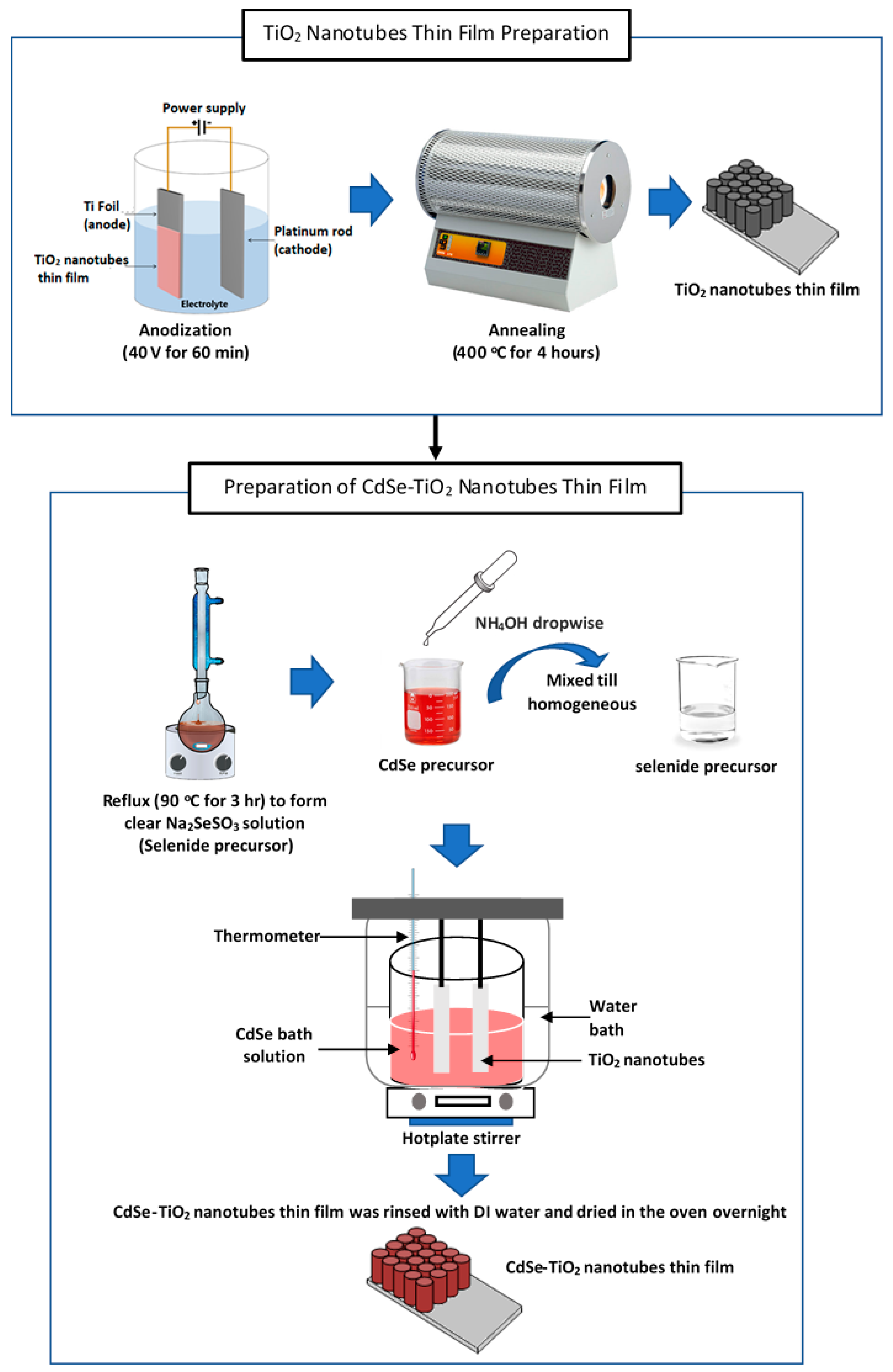
2.1. Preparation of TiO2 Nanotube Thin Films

The TiO2 nanotube thin films were prepared by the electrochemical method of anodizing Ti foils in a two-electrode cell at 40 V for 60 min, consisting of Ti foil as the working electrode and platinum rod as the counter electrode (Figure 1). The electrolyte comprised of ethylene glycol, 0.3 wt % ammonium fluoride, and 5 wt % hydrogen peroxide. The anodized samples were rinsed with deionized (DI) water and subsequently annealed for 4 h in the air at 400 °C with a heating rate of 5 °C/min−1, and cooled naturally to achieve the pure anatase phase of TiO2 [35].

2.2. Preparation of CdSe–TiO2 Nanotube Thin Films

The CdSe was deposited on the TiO2 nanotube thin films via CBD, as shown in the schematic diagram in Figure 1. To prepare the 5 mM CdSe solution precursor, the selenide precursor (Na2SeSO3 solution) was prepared by mixing 0.6 M sodium sulfite with 0.2 M selenium metal powder in DI water. The mixture was heated under reflux at 90 °C for 3 h to form a clear Na2SeSO3 solution. The cadmium precursor was prepared by dissolving 0.2 M of Cd(CH3COO)2∙2H2O in DI water. Then, a concentrated ammonia solution (30%) was added into the cadmium solution slowly to adjust the pH of the solution between 12 to 12.5. This was to prevent a reverse reaction of Cd(NH3)42+ to form stable cadmium hydroxide (Cd(OH)2). Both precursor solutions were then mixed until homogenous. The annealed anatase TiO2 nanotube thin films were soaked vertically inclined into the CdSe bath solution for the deposition process for 1 h. The deposition temperature was varied from 20 to 60 °C. A digital programmable hotplate (Torrey Pines Scientific) was used in this experiment. The temperature of the chemical bath was set and, upon the deposition process, the solution’s temperature was checked, using a thermometer for confirmation. Throughout the deposition process, the temperature of the chemical bath was checked from time to time. Then, the samples were the rinsed with DI water and dried in an oven overnight.

2.3. Characterizations

The surface and cross-sectional morphologies of the prepared samples (TiO2 nanotube thin films and CdSe/TiO2 nanotube thin films) were investigated via field emission scanning electron microscopy (FE-SEM, JEO JSM 7600-F, JOEL Ltd., Tokyo, Japan) while the elemental analysis was conducted using Oxford Instruments by means of energy dispersive X-ray spectroscopy (EDX, Oxford Instruments, Abingdon, United Kingdom) The phase transition and crystallinity of all prepared samples was studied using X-ray diffraction (XRD, Bruker AXS D8 Advance, Bruker, Karlsruhe, Germany)and a Raman spectrometer (Renishaw inVia, Renishaw, Wotton-under-Edge, United Kingdom)In this study, XRD was operated using Cu Kα radiation (λ = 0.1546 nm) at a scanning rate of 2° min−1 over the angles 2θ = 20° to 70°. The Raman spectroscopy was operated at an excitation wavelength of 532 nm generated by an Ar ion laser over the range of 100 to 1000 cm−1. The binding energy and chemical state of the samples were measured and quantified with X-ray photoelectron spectroscopy (XPS, PHI Quantera II, Physical Electronic, Minnesota, USA) with an Al cathode scan (hv = 1486.8 eV) of 100 microns and 280 eV with pass energy. The precise analysis of the features of each element was decomposed in the Shirley background using the Voigt curve fitting function. The optical properties of the prepared samples were recorded using a UV-Vis diffused reflectance spectrophotometer (Shimadzu UV-2700 UV-Vis, Shimadzu, Kyoto, Tokyo) from 240 to 800 nm.

2.4. Photoelectrochemical Testing

A three-electrode system composed of Pt as the counter electrode, Ag/AgCl (3 M KCl) as the reference electrode, and the prepared samples as the working electrode were used in a 1 M KOH aqueous electrolyte. The photoelectrochemical measurement of the prepared samples was evaluated by linear sweep voltammetry using a potantiostat (Autolab PGSTAT 204, Metrohm, Herisau, Switzerland) and illuminated by a 150 W Xenon lamp (Zolix LSP-X150, Zolix Instruments CO., Ltd., Beijing, China) with a light intensity of 100 mW cm−2 focusing on the dipped part of the electrode.

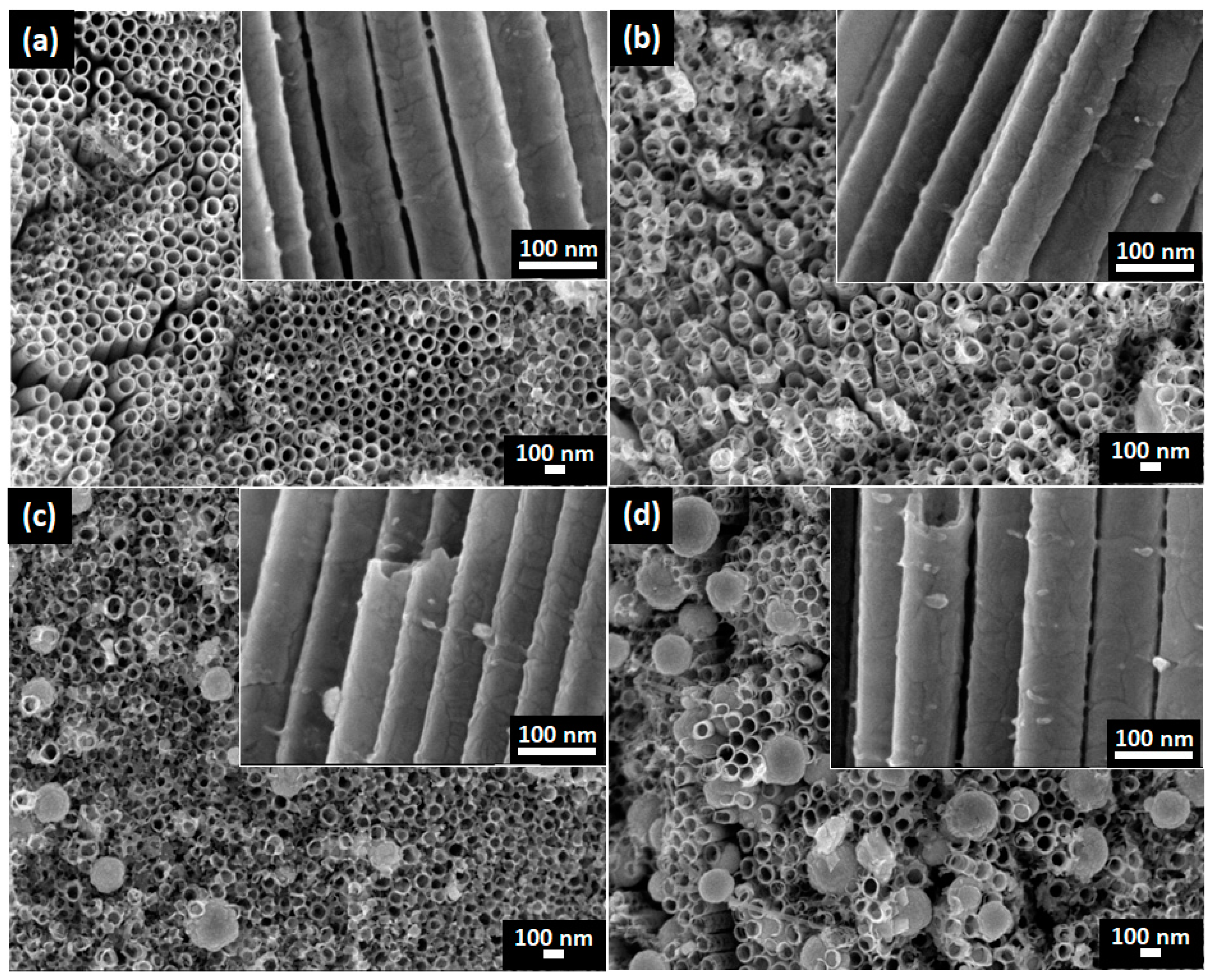
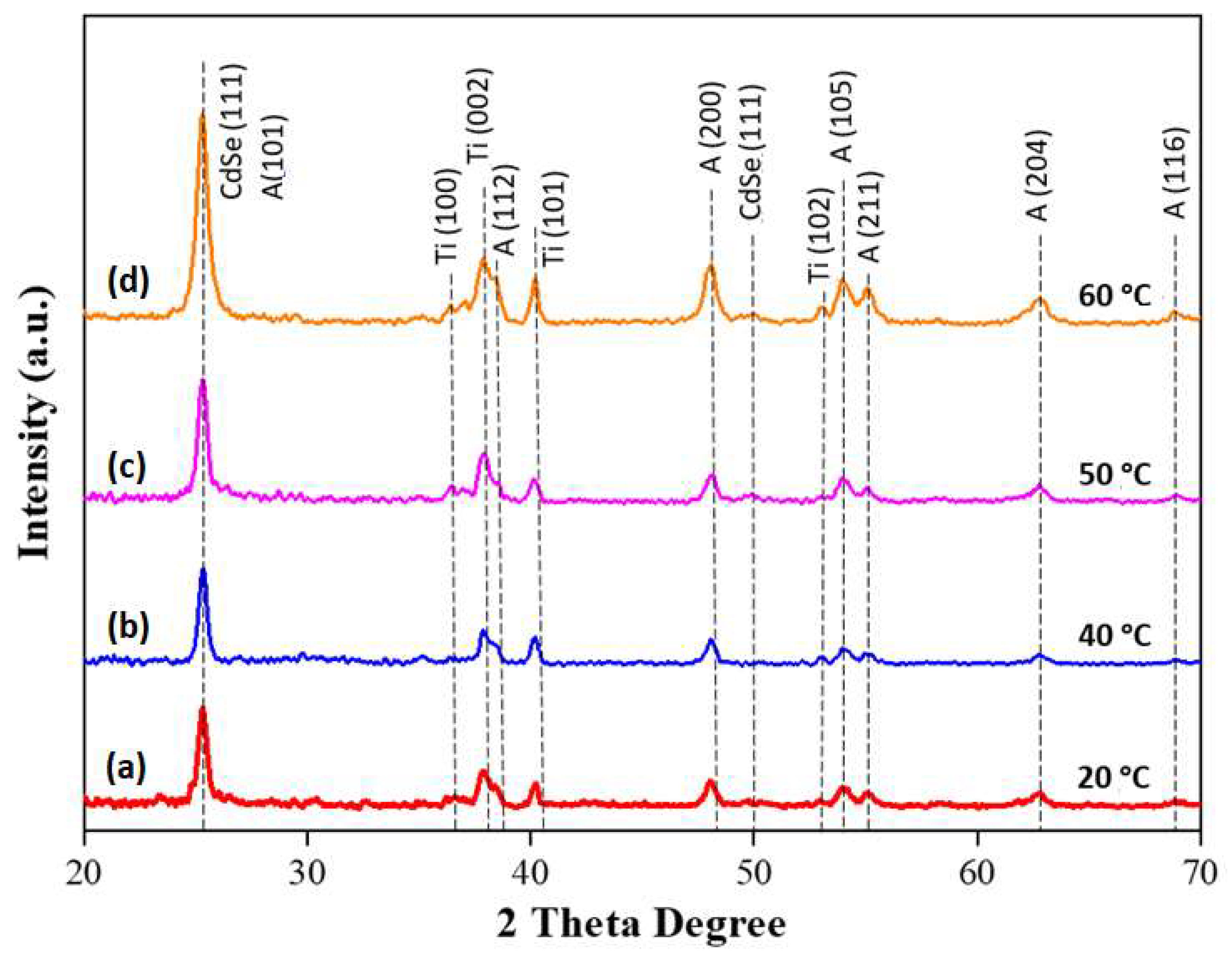
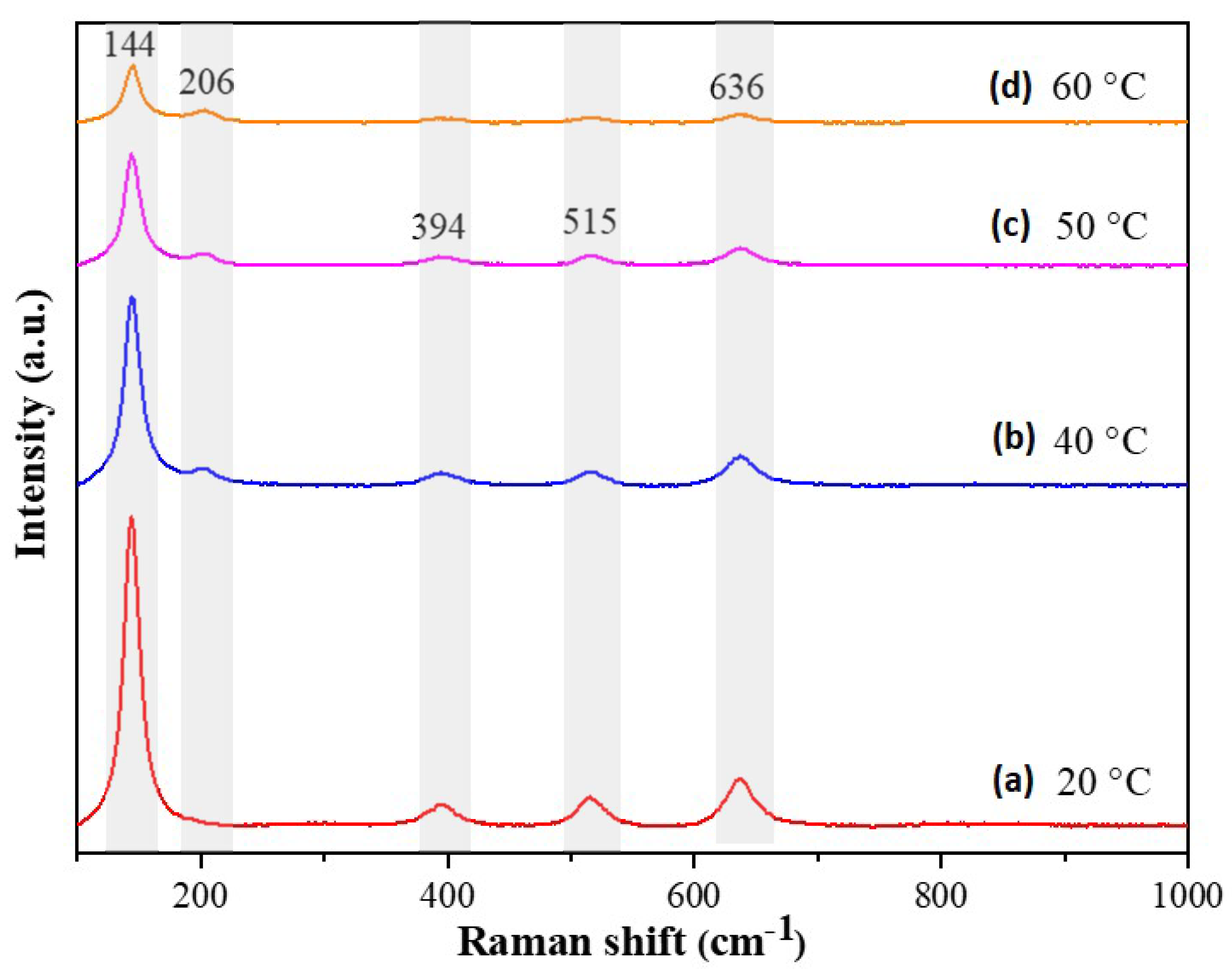
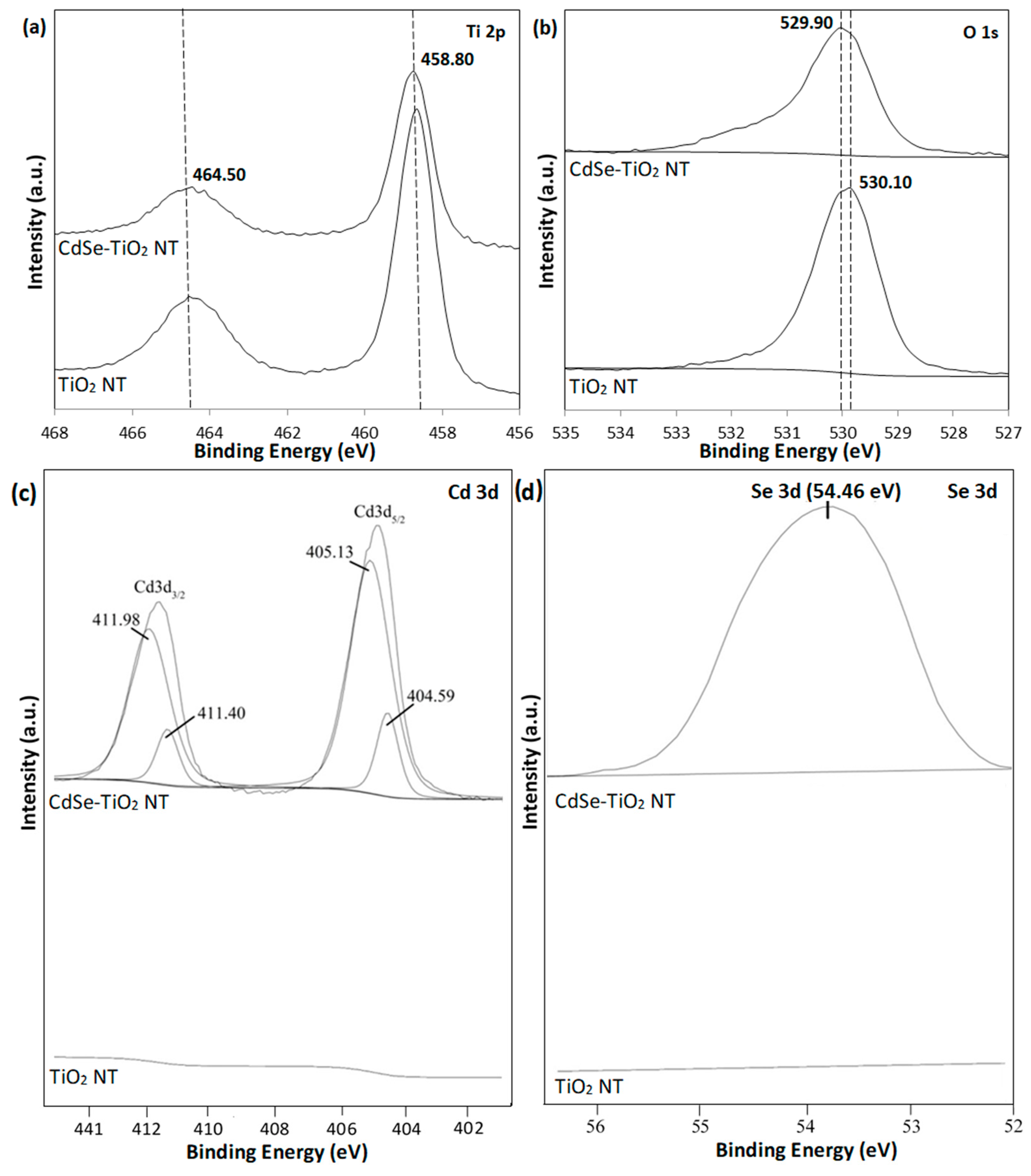
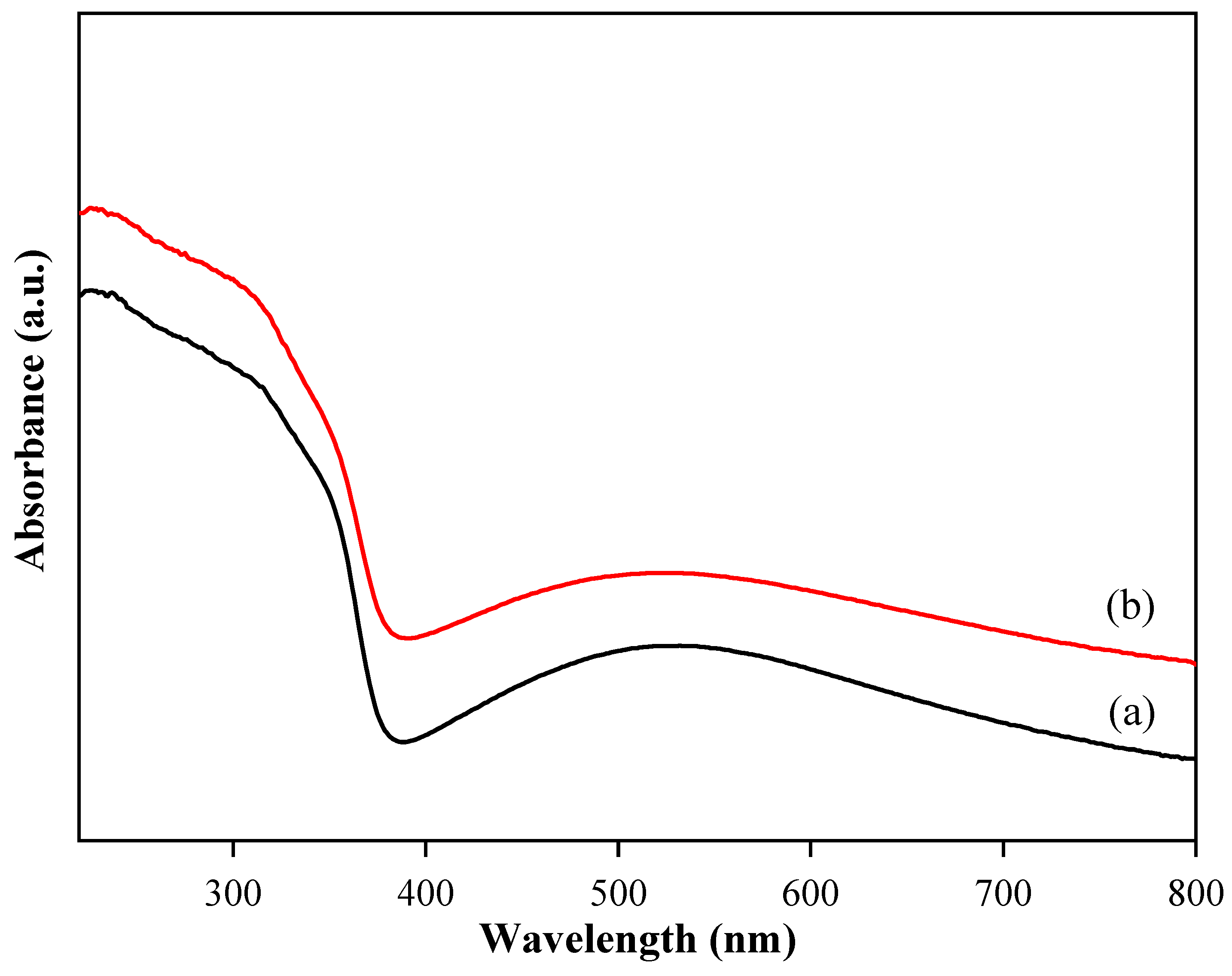
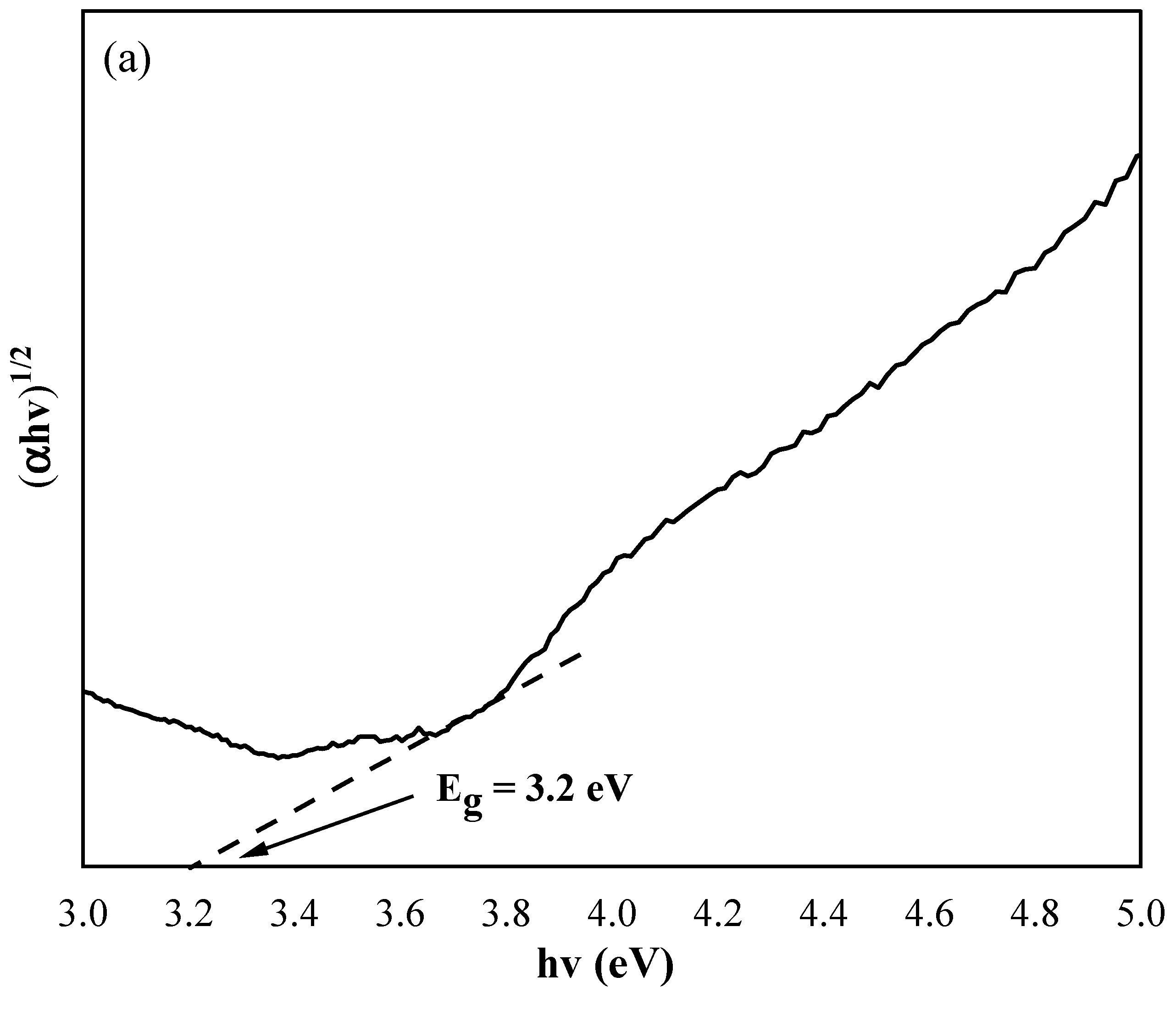
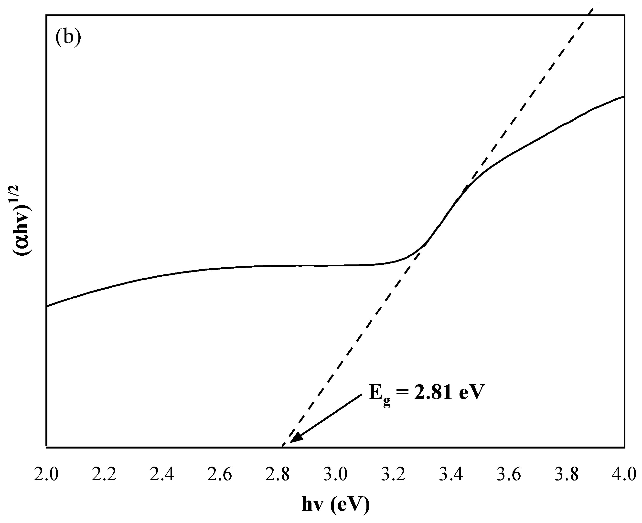
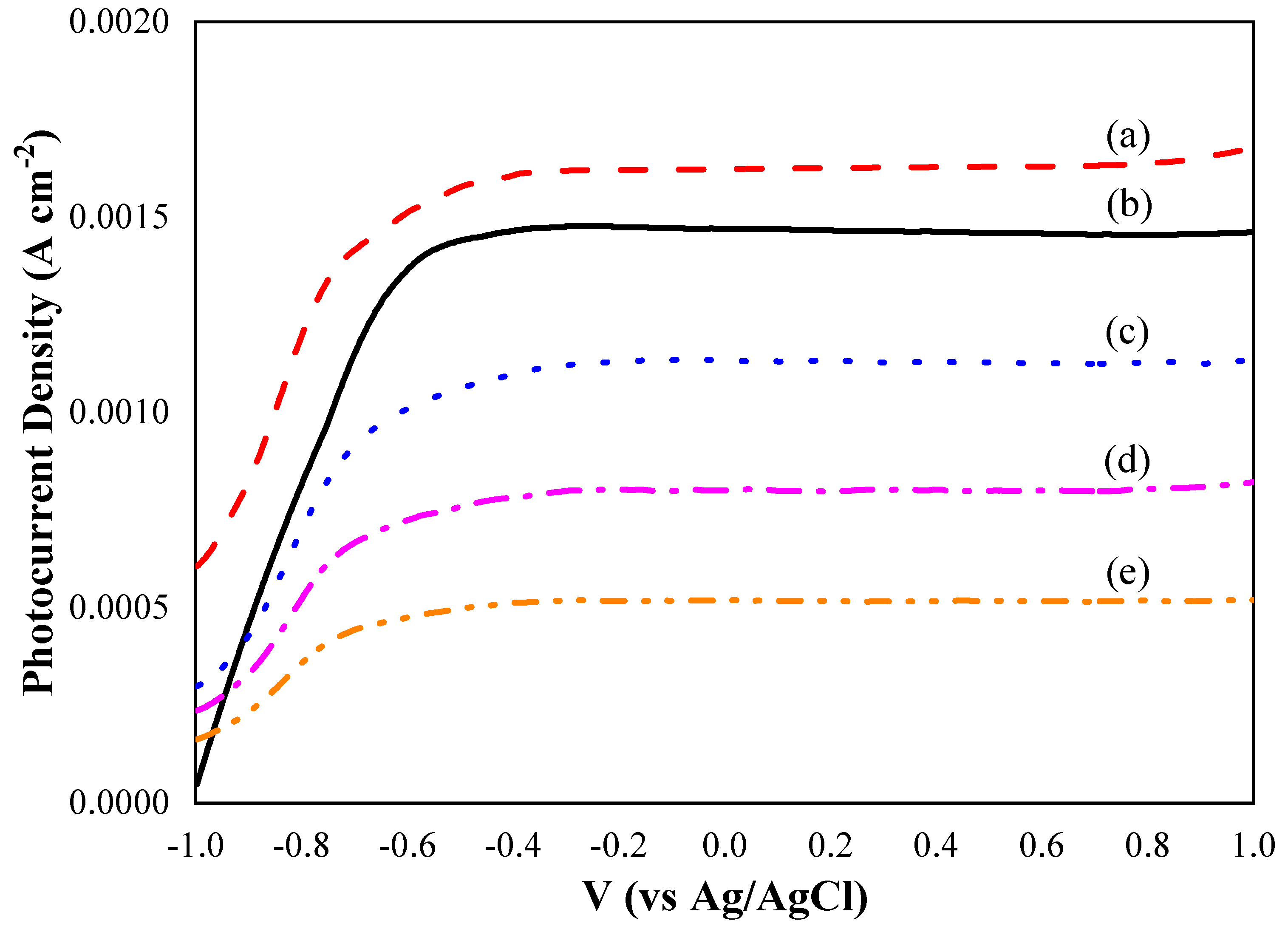
3. Results and Discussion

The surface and cross-section morphologies of all the prepared CdSe–TiO2 nanotube thin film samples deposited at various temperatures from 20 to 60 °C are shown in Figure 2a–d. The highly ordered TiO2 nanotube thin films were successfully synthesized in our previous report, with an average inner-tube diameter and tube length of 76 nm and 5.6 µm, respectively [21,47]. In this study, a clear surface morphology change was observed for all samples as function to the chemical bath temperature. At a low temperature (20 °C), the deposition of CdSe on the TiO2 nanotube thin films was almost negligible, as shown in Figure 2a. However, the average inner-tube’s diameter of the sample decreased to 71 nm upon the deposition of CdSe, indicating that the nucleation process had taken place on the sample. A low chemical bath temperature of 20 °C led to a low deposition rate, thus, slowing the nuclei growth on the TiO2 nanotube thin films. As the chemical bath temperature increased to 40 °C, the presence of CdSe particles was observed, with an average inner-tube diameter of 90 nm, which partially covered the nanotubes (refer to Figure 2b). Moreover, the tube’s diameter decreased to 68 nm upon the deposition of CdSe on the TiO2 nanotube thin films. The agglomeration of CdSe into larger particles was observed when the chemical bath temperature increased to 50 and 60 °C. They were uniformly dispersed on the surface of the nanotubes with an average diameter of 145 nm at chemical bath temperatures of 50 °C and 220 nm at 60 °C. Furthermore, the agglomeration of CdSe covered most of the nanotube circumferences, as shown in Figure 2c–d. The average tube diameters of the samples were found to decrease to 57 nm (50 °C) and 54 nm (60 °C). The cross-sectional morphologies (inset figures) showed an adhesive texture, with the presence of CdSe particles deposited throughout the wall surface. This indicates that the deposition of CdSe took place on the top surface and the wall surface of the nanotubes. The EDX analysis confirmed the presence of cadmium (Cd), selenium (Se), titanium (Ti), and oxygen (O) elements in all samples, as shown in Table 1. These results supported the observation from the FE-SEM results, as the elemental composition of Cd and Se increased as the chemical bath temperature increased. In addition, the ratio of the Cd and Se elements in all samples was 1:1, thereby confirming the deposition of stoichiometry CdSe on the TiO2 nanotube thin films.
Figure 3 shows the XRD patterns for the CdSe–TiO2 nanotube thin films deposited at different chemical bath temperatures at 2θ = 20° to 70°. All samples exhibited an intense peak of CdSe at 2θ = 25.35°, which corresponded to the (1 1 1) preferred orientation of a cubic phase of CdSe (JCPDS No.: 19–0191). This peak was found to overlap with the peak of the anatase crystal plane at 2θ = 25.37° (1 0 1) phase. The intensity of the peak increased as function of the chemical bath temperature, which indicated an abundancy of the CdSe and the well crystalline nature of the CdSe [44]. These results were agreeable with the FE-SEM analysis, as the chemical bath temperature increased as the amount of CdSe deposited onto the TiO2 nanotube thin films increased. A small peak was observed at 2θ = 49.7°, corresponding to a (3 1 1) plane of cubic zinc blended phase CdSe in the CdSe–TiO2 nanotube thin films deposited at the chemical bath temperatures of 50 and 60 °C. However, the peak was not detected in the CdSe–TiO2 nanotube thin films deposited at low chemical bath temperatures due to the low content of CdSe (< 2 at % from EDX analysis) in the sample, which was too insufficient to be detected by XRD analysis [48,49,50]. The single phase of TiO2 crystal indexed to anatase planes (JCPDS No.: 21–1272) was observed at 2θ = 38.67°, 48.21°, 54.10°, 55.26°, 62.66°, and 68.74°, corresponding respectively to planes (1 1 2), (2 0 0), (1 0 5), (2 1 1), (2 0 4), and (1 1 6). In addition, the peaks at 2θ = 35.1°, 38.4°, 40.2°, and 53.0° corresponded to (1 0 0), (0 0 2), (1 0 1), and (1 0 2), and were originated from a Ti metal substrate (JCPDS no.: 44–1294).
The Raman spectra of the CdSe–TiO2 nanotube thin films (shown in Figure 4) further confirmed the presence of cubic CdSe phase in the samples. The characteristic peaks of the anatase phase of TiO2 were observed at 144, 394, 515, and 636 cm−1, corresponding to Eg, B1g, A1g, and Eg vibration modes. The Eg vibration mode was mainly caused by symmetric stretching vibration, while B1g was due to the symmetric bending vibration, and A1g was caused by the anti-symmetric bending of O–Ti–O in TiO2 [46,51]. A gradual decrease in the intensity of these peaks was observed with an increase of the chemical bath temperature due to the increase of cubic CdSe content in the samples. The samples prepared at chemical bath temperatures of 40, 50, and 60 °C showed presence of a Raman shift at 206 cm−1, corresponding to the first order for the longitudinal optical phonon (LO) of cubic CdSe.
The surface chemical state of pure TiO2 nanotube thin films and CdSe–TiO2 nanotube thin films was investigated using XPS analysis. Figure 5 displays the XPS spectra of both samples, which mainly consisted of Ti 2p, O 1s, Cd 3d, and Se 3d elements. Two broad peaks centered at 458.80 and 464.50 eV are observed in Figure 4a, corresponding to the Ti 2p3/2 and Ti 2p1/2 peaks of Ti4+ in the TiO2 nanotube thin films [39]. The intensity of both peaks gradually decreased upon the deposition of CdSe into the TiO2 nanotube thin films, indicating the presence of CdSe in the TiO2 lattice structure. However, the deposition of CdSe on TiO2 did not affect the Ti chemical state of the nanotubes. In contrast, the O 1s elements showed a slight shift from 530.90 eV for the pure TiO2 nanotube thin film samples to 529.90 eV for the CdSe–TiO2 nanotube thin film samples due the strong interaction between CdSe clusters and TiO2 nanotube thin films. The strong interaction bond between CdSe and TiO2 served as the heterojunctions that became captives of the electron/hole pairs from the CdSe clusters [38]. Hence, this will suppress the recombination of the electron/hole and photoelectrochemical activity.
Figure 5c illustrates the double peak features of the Cd 3d spectra for the CdSe–TiO2 nanotube thin film sample, suggesting the presence of Cd element in the sample, while no traces of Cd element were observed in the TiO2 nanotube thin film sample. The precise assessment of the functions of the spin-orbital split Cd 3d5/2 and Cd 3d3/2 were disintegrated by using the Voigt curve fitting function within the Shirley background. Four peaks were observed, centered at 405.13 and 404.59 eV corresponding to Cd 3d5/2, whereas the binding energy at 411.98 and 411.40 eV corresponded to Cd 3d3/2. The prominent binding energy centered at 405.13 and 411.98 eV, which was due to the core level of Cd2+ cations of the CdSe crystal structure [41]. The additional peaks observed with lower intensities of 405.13 and 411.98 had a weak shift in peak positions. CdO formation was also proved in CdSe, where the core levels of the oxidation of Cd were weak at the 3d5/2 and 3d3/2 core levels [51,52]. The small CdO volume could, therefore, be verifiable using the CBD technique from low intensity peaks with 404.59 and 411.40 bonding energy. The existence of the Se element in the CdSe–TiO2 nanotube thin films sample was proved from the Se 3d spectra shown in Figure 5d. A broad peak centered at 54.46 eV represented that the Se 3d3/2 characteristic was due to the Se2− anions of CdSe [53,54].
The optical properties of pure TiO2 nanotube thin films and CdSe–TiO2 nanotube thin films were carried out using a UV-Vis diffuse reflectance analysis (DRS). The adsorption spectra for both samples are shown in Figure 6. The adsorption edge of pure TiO2 nanotube thin films was observed below 400 nm due to the excitation of the electron from the valence band to the conduction band [54]. However, the CdSe–TiO2 nanotube thin films showed an adsorption above 400 nm, suggesting that more visible light was adsorbed by the sample, hence facilitating the generation of a high amount of carrier charge, which then enhanced the photocurrent response of the sample. The Tauc approach was used to determine the optical bandgap of the pure TiO2 nanotube thin films and CdSe–TiO2 nanotube thin film samples using the equation below:
α = α 0 h v E g h v
where Eg is the separation between the bottom of the conduction band and the top of the valance band, hv is the photon energy, and n is the constant. In this case, n = ½, which follows a direct transition. The plot of (αhv)1/2 against hv for the pure TiO2 nanotube thin films and CdSe–TiO2 nanotube thin films are shown in Figure 7. The band gap of pure TiO2 nanotube thin films and CdSe–TiO2 nanotube thin films were estimated from the intersection of the baseline with the tangent line of the sharply decreasing region of the spectra. It was noted that the band gap of the pure TiO2 nanotube thin films was 3.20 eV, while the band gap of the CdSe–TiO2 nanotube thin films was 2.81 eV. It was well known that the CdSe bulk sample band gap was 1.74 eV. Typically, the band gap of CdSe varies with the deposition method and deposition parameters, and is also attributed due to the changes in the film composition and structural defects. In this case, the large band gap of the CdSe–TiO2 nanotube thin films corresponded to the low amount of CdSe on the TiO2 nanotube thin films, as discussed in the EDX results.
A photoelectrochemical analysis of pure TiO2 nanotube thin films and CdSe–TiO2 nanotube thin films deposited at chemical bath temperatures from 20 to 60 °C was performed using linear sweep potential voltammetry with applied potential from −1 to 1 V versus Ag/AgCl in a 1 M KOH aqueous electrolyte. Figure 8 shows the Jp-V curves for all samples. Upon irradiation, the photocurrent density of CdSe–TiO2 nanotube thin films deposited at 20 °C showed the highest photocurrent density value at 1.70 mA cm−2, which was 17 % higher than the pure TiO2 nanotube thin films (1.45 mA cm−2). However, the CdSe–TiO2 nanotube thin films deposited at higher chemical bath temperatures exhibited a decrease in photocurrent density, with 1.1 mA cm−2, 1.8 mA cm−2, and 0.5 mA cm−2 for the samples deposited at temperatures of 40, 50, and 60 °C, respectively. The obtained photocurrent density was much higher compared to other TiO2 thin film-based photoelectrochemical cells that were reported earlier: Gd@TiO2 NRA (~0.51 mA cm−2) [30], TiO2/g-C3N4 (~0.85 mA cm−2) [55], TiO2/WO3 (~1.00 mA cm−2) [56], and CdSe–TiO2 (~1.6 mA cm−2) [57].
The obtained results indicated that the low loading of CdSe on the TiO2 nanotube thin films was sufficient to enhance the photocurrent density of the sample. Furthermore, the CdSe–TiO2 nanotube thin films deposited at a temperature of 20 °C showed a clear surface morphology without any clogged nanotubes. Therefore, the sample experienced better ion diffusion, thus, enhancing the photocurrent density of the sample. Generally, the CdSe species in the sample acted as an effective electron acceptor, which generated an energy band below the conduction band of TiO2. Thus, the photogenerated electrons from TiO2 will be captured by the CdSe species due to the interpretation of inter-band states with key redox potential, or surface states within the corresponding energetic position. In contrast, in pure TiO2 nanotube thin films, the photo-induced electron in the conduction band was trapped for the recombination with holes. In this study, excessive loading of the CdSe species on the TiO2 nanotube thin films exhibited poor photocurrent density. As discussed in the FE-SEM results, the CdSe–TiO2 nanotube thin films deposited at temperatures of 40 to 60 °C displayed agglomerated CdSe particles, where they mostly covered the TiO2 nanotube thin film circumstances and led to poor ion diffusion throughout the nanotubes during the photocurrent analysis. This condition prevented the electron transport throughout the sample and resulted in low photocurrent density [58,59]. Thus, the enhancement of photocurrent density under solar illumination was ascribed to the optimum content of the CdSe species incorporated into the lattice of TiO2.

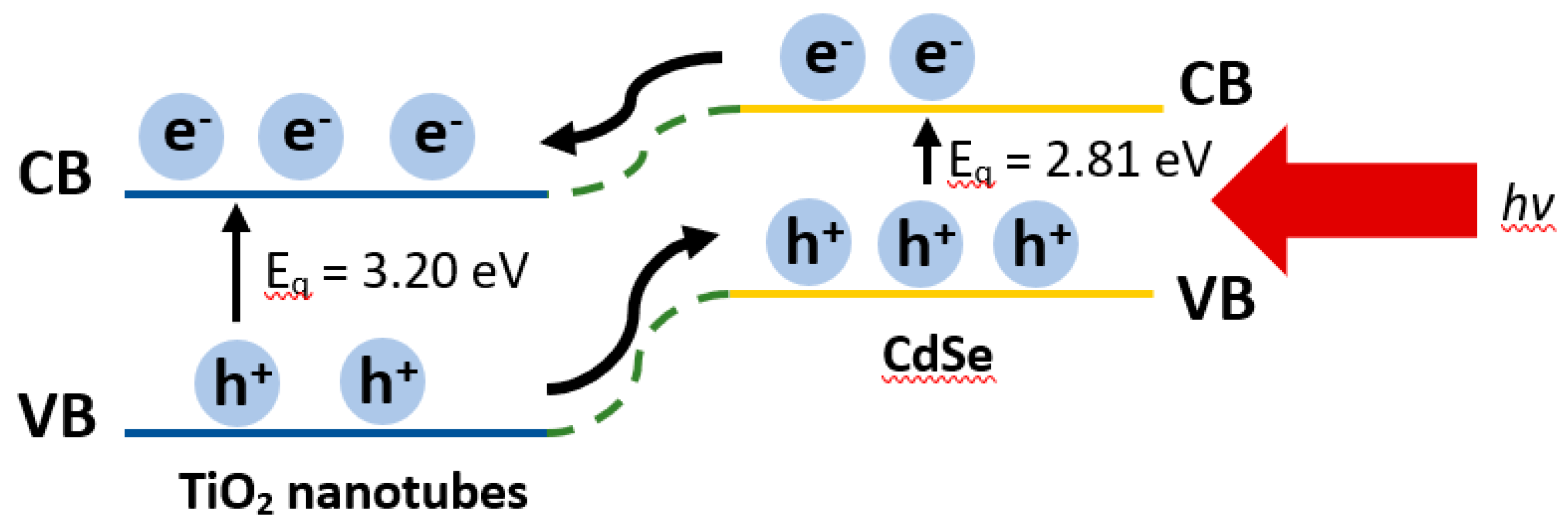
Mechanism Study of CdSe–TiO2 Nanotubes via CBD Method

CBD consists of two important steps, which are the nucleation process and particle growth. This method is based on the formation of the solid phase from a precursor solution. During the deposition process, the first stage corresponds to the initiation of the critical nuclei of the species. In this study, a bath solution with a Cd2+ and Se2− precursor was used to deposit CdSe on the TiO2 nanotube thin films. The mechanisms of the CdSe formation during the CBD have been described in our previous report [37]. Cd(CH3COO)2·2H2O will form a Cd complex with ammonia solution to finally form Cd2+.
Cd ( CH 3 COO ) 2 + 2 NH 4 OH Cd ( OH ) 2 + 2 NH 4 ( CH 3 COO )
Cd ( OH ) 2 + 4 NH 2 OH Cd ( NH 3 ) 4 2 + + 2 OH + + 4 H 2 O
Cd ( NH 3 ) 4 2 + Cd 2 + + 4 NH 3
In addition, Na2SeSO3 will hydrolyze in the solution to produce Se2-, as presented below:
Na 2 SeSO 3 + OH Na 2 SO 4 + HSe
HSe + OH Se 2 + H 2 O
The Cd(NH3)22+ then reacts with Se2- to form a CdSe species to be deposited on the TiO2 nanotube thin films.
Cd ( NH 3 ) 4 2 + + Se 2 CdSe + 4 NH 3
The formation of CdSe and the deposition of the species on the TiO2 nanotube thin films will occur simultaneously in the chemical bath. The rate of deposition will depend on the deposition parameters, such as chemical bath temperature, pH, precursor’s concentration, and deposition time. The CdSe nuclei will form and initiate the deposition process on the TiO2 nanotube thin film surfaces. During this stage, the metastability of the precursor solution system is not affected by the emerging nuclei. As the deposition process progresses, the intermediate stage, which comprises a combination process of growth of the existing CdSe particles, and the initiation of additional nuclei will reduce the metastability of the precursor solution system. These processes will resume until the end of the deposition process.
Figure 9 shows a simple schematic diagram representing the carrier transfer processes between CdSe and the TiO2 nanotubes, which can aid the understanding of the PEC mechanism. When the solar light illuminates, both TiO2 and CdSe harvest photons and generate electron-hole pairs. The conduction band (CB) of CdSe is more positive than the TiO2 nanotubes, therefore, the photo-induced electrons in the CB of CdSe will transfer to the CB of the TiO2 nanotubes and further move along the TiO2 nanotubes, to the external circuitry [40,59,60]. Simultaneously, the left holes in the valance band (VB) of TiO2 will transfer to the VB of CdSe. Therefore, this results in a parallel array of rapid transfer pathways for carrier transportation. The band gap narrowing, which improvises the visible light absorption, will provide more sites that can slow down the recombination of charge carriers [50,51,61]. The holes migrating to the surface of CdSe will react with the electrolyte at the interface between the photoanode and the electrolyte [59]. Based on the aforementioned scenario, CdSe has two advantages: first, CdSe enhances the photon-induced charge separation rate by widening the response spectrum compared with the TiO2 nanotubes; second, the heterojunction that anchors CdSe on the surface of the TiO2 nanotubes provides additional channels for the separated charge transportation thanks to the specific band potential distribution and the charge transfer property, so that the recombination probability decreases, which results in a higher PEC performance of the sample. In short, the PEC properties of the CdSe–TiO2 nanotubes are demonstrated to be controllable through the chemical bath deposition’s temperature.

4. Conclusions

In summary, CdSe–TiO2 nanotube thin films were successfully synthesized using CBD by controlling the chemical bath temperature. The particle size and CdSe loading on the TiO2 nanotube thin films were controlled by varying the chemical bath temperature from 20 to 60 °C. The CdSe–TiO2 nanotube thin films showed an excellent photo response in the visible light region, thus, facilitating the generation of a high amount of carrier charge. The highest photocurrent density of 1.70 mA cm−2 was obtained by the CdSe–TiO2 nanotube thin films deposited at 20 °C, which affirmed that low loading of CdSe on the TiO2 nanotube thin films was sufficient to enhance the photocurrent of the sample. This study has brought light to the CdSe–TiO2 nanotube thin films as promising materials for photoelectrochemical cell application.

Author Contributions

Conceptualization, Supervision, Funding acquisition, Writing – review and editing, C.W.L.; Writing – original draft preparation, Formal analysis, N.A.S.; Writing – original draft preparation, F.W.L.; Experimental, Formal analysis, N.A.A.S.; Experimental, Formal analysis, K.S.L., Writing – review and editing, P.M.C.; Writing – review and editing, Funding acquisition, S.K.T.; Writing - review and editing, Funding acquisition, N.A. All authors have read and agreed to the published version of the manuscript.

Funding

This research work was financially supported by the Global Collaborative Programme - SATU Joint Research Scheme (No. ST012-2019), Impact-Oriented Interdisciplinary Research Grant (No. IIRG018A-2019) from University of Malaya, Internal Research Grant Opex (No. RJ010517919/iRMC/Publication) and BOLD2025 Grant (No. 10436494/B/2019097) under Universiti Tenaga Nasional.

Acknowledgments

The authors would like to acknowledge the Institute for Advanced Studies (IAS), University of Malaya and MIMOS Failure Analysis Lab for the provision of the laboratory and materials characterization facilities.

Conflicts of Interest

The authors declare no conflict of interest.

References

  1. Hassan, F.U.; Ahmed, U.; Muhyuddin, M.; Yasir, M.; Ashiq, M.N.; Basit, M.A. Tactical modification of pseudo-SILAR process for enhanced quantum-dot deposition on TiO2 and ZnO nanoparticles for solar energy applications. Mater. Res. Bull. 2019, 120, 110588. [Google Scholar] [CrossRef]
  2. Kleiman, A.; Meichtry, J.; Vega, D.; Litter, M.; Márquez, A. Photocatalytic activity of TiO2 films prepared by cathodic arc deposition: Dependence on thickness and reuse of the photocatalysts. Surf. Coat. Technol. 2020, 382, 125154. [Google Scholar] [CrossRef]
  3. Lim, Y.P.; Lim, Y.C. Synthesis of Hybrid Cu-Doped TiO2 Photocatalyst for Dye Removal. in Key Engineering Materials. Trans. Tech. Publ. 2019, 797, 84–91. [Google Scholar]
  4. Özcan, L.; Mutlu, T.; Yurdakal, S. Photocatalytic degradation of Paraquat by pt loaded TiO2 nanotubes on Ti anodes. Materials 2018, 9, 1715. [Google Scholar] [CrossRef] [Green Version]
  5. Shikoh, A.S.; Ahmad, Z.; Touati, F.; Shakoor, R.; Al-Muhtaseb, S.A. Optimization of ITO glass/TiO2 based DSSC photo-anodes through electrophoretic deposition and sintering techniques. Ceram. Int. 2017, 43, 10540–10545. [Google Scholar] [CrossRef]
  6. Hong, S.-T.; Lin, L.-Y. Fabrication of TiO2 nanoparticle/TiO2 microcone array photoanode for fiber-type dye-sensitized solar cells: Effect of acid concentration on morphology of microcone. Electrochim. Acta 2020, 331, 135278. [Google Scholar] [CrossRef]
  7. Low, F.W.; Lai, C.W.; Hamid, S.B.A. Study of reduced graphene oxide film incorporated of TiO2 species for efficient visible light driven dye-sensitized solar cell. J. Mater. Sci. Mater. Electron. 2016, 28, 3819–3836. [Google Scholar] [CrossRef]
  8. Low, F.W.; Lai, C.W.; Hamid, S.B.A. Surface modification of reduced graphene oxide film by Ti ion implantation technique for high dye-sensitized solar cells performance. Ceram. Int. 2017, 43, 625–633. [Google Scholar] [CrossRef]
  9. Low, F.W.; Lai, C.W.; Lee, K.M.; Juan, J.C. Enhance of TiO2 dopants incorporated reduced graphene oxide via RF magnetron sputtering for efficient dye-sensitised solar cells. Rare Met. 2018, 37, 919–928. [Google Scholar] [CrossRef]
  10. Low, F.W.; Lai, C.W. Reduced Graphene Oxide Decorated Tio2 for Improving Dye-Sensitized Solar Cells (DSSCs). Curr. Nanosci. 2019, 15, 631–636. [Google Scholar] [CrossRef]
  11. Haring, A.; Morris, A.; Hu, M. Controlling morphological parameters of anodized titania nanotubes for optimized solar energy application. Materials 2012, 5, 1890–1909. [Google Scholar] [CrossRef] [Green Version]
  12. Nguyen, V.N.; Nguyen, M.V.; Nguyen, T.H.T.; Doan, M.T.; Ngoc, L.L.T.; Janssens, E.; Yadav, A.; Lin, P.C.; Nguyen, M.S.; Hoang, N.H. Surface modified titanium dioxide nanofibers with gold nanoparticles for enhance photoelectrochemical water splitting. Materials 2020, 10, 261. [Google Scholar]
  13. Wang, Q.; Sun, C.; Liu, Z.; Tan, X.; Zheng, S.; Zhang, H.; Wang, Y.; Gao, S. Ultrasound-assisted successive ionic layer adsorption and reaction synthesis of Cu2O cubes sensitized TiO2 nanotube arrays for the enhanced photoelectrochemical performance. Mater. Res. Bull. 2019, 111, 277–283. [Google Scholar] [CrossRef]
  14. Lim, Y.-C.; Zainal, Z.; Tan, W.-T.; Hussein, M.Z.; Chin, L.Y. Anodization Parameters Influencing the Growth of Titania Nanotubes and Their Photoelectrochemical Response. Int. J. Photoenergy 2012, 2012, 1–9. [Google Scholar] [CrossRef]
  15. Ahmed, A.M.; Mohamed, F.; Ashraf, A.M.; Shaban, M.; Khan, A.A.P.; Asiri, A.M. Enhanced photoelectrochemical water splitting activity of carbon nanotubes@TiO2 nanoribbons in different electrolytes. Chemosphere 2020, 238, 124554. [Google Scholar] [CrossRef]
  16. Samsudin, N.A.; Zainal, Z.; Lim, H.N.; Sulaiman, Y.; Chang, S.-K.; Lim, Y.-C.; Amin, W.N.M. Enhancement of Capacitive Performance in Titania Nanotubes Modified by an Electrochemical Reduction Method. J. Nanomater. 2018, 2018, 1–9. [Google Scholar] [CrossRef]
  17. Qorbani, M.; Khajehdehi, O.; Sabbah, A.; Naseri, N. Ti-rich TiO2 Tubular Nanolettuces by Electrochemical Anodization for All-Solid-State High-Rate Supercapacitor Devices. ChemSusChem 2019, 12, 4064–4073. [Google Scholar] [CrossRef]
  18. Heng, I.; Lai, C.W.; Juan, J.C.; Numan, A.; Iqbal, J.; Teo, E.Y.L. Low-temperature synthesis of TIO2 nanocrystals for high performance electrochemical supercapacitors. Ceram. Int. 2019, 45, 4990–5000. [Google Scholar] [CrossRef]
  19. Heng, I.; Low, F.W.; Lai, C.W.; Juan, J.C.; Amin, N.; Tiong, S.K. High performance supercapattery with rGO/TiO2 nanocomposites anode and activated carbon cathode. J. Alloy. Compd. 2019, 796, 13–24. [Google Scholar] [CrossRef]
  20. Seekaew, Y.; Wisitsoraat, A.; Phokharatkul, D.; Wongchoosuk, C. Room temperature toluene gas sensor based on TiO2 nanoparticles decorated 3D graphene-carbon nanotube nanostructures. Sens. Actuators B Chem. 2019, 279, 69–78. [Google Scholar] [CrossRef]
  21. Lai, C.W.; Sreekantan, S. Study of WO3 incorporated C-TiO2 nanotubes for efficient visible light driven water splitting performance. J. Alloy. Compd. 2013, 547, 43–50. [Google Scholar] [CrossRef]
  22. Momeni, M.M.; Ghayeb, Y.; Ezati, F. Fabrication, characterization and photoelectrochemical activity of tungsten-copper co-sensitized TiO2 nanotube composite photoanodes. J. Colloid Interface Sci. 2018, 514, 70–82. [Google Scholar] [CrossRef] [PubMed]
  23. Ayal, A.K.; Zainal, Z.; Lim, H.N.; Talib, Z.A.; Lim, Y.-C.; Chang, S.-K.; Holi, A.M. Fabrication of CdSe nanoparticles sensitized TiO 2 nanotube arrays via pulse electrodeposition for photoelectrochemical application. Mater. Res. Bull. 2018, 106, 257–262. [Google Scholar] [CrossRef]
  24. Tsui, L.-K.; Saito, M.; Homma, T.; Zangari, G. Trap-state passivation of titania nanotubes by electrochemical doping for enhanced photoelectrochemical performance. J. Mater. Chem. A 2015, 3, 360–367. [Google Scholar] [CrossRef]
  25. Diaz-Real, J.; Elsaesser, P.; Holm, T.; Mérida, W. Electrochemical reduction on nanostructured TiO2 for enhanced photoelectrocatalytic oxidation. Electrochimica Acta 2020, 329, 135162. [Google Scholar] [CrossRef]
  26. Cortes, M.A.L.R.M.; McMichael, S.; Hamilton, J.W.J.; Sharma, P.K.; Brown, A.; Byrne, J.A. Photoelectrochemical reduction of CO2 with TiNT. Mater. Sci. Semicond. Process. 2020, 108, 104900. [Google Scholar] [CrossRef]
  27. Pang, Y.; Feng, Q.; Kou, Z.; Xu, G.; Gao, F.; Wang, B.; Pan, Z.; Lv, J.; Zhang, Y.; Wu, Y. Surface precleaning strategy intensifies interface coupling of Bi2O3/TiO2 heterostructure for enhanced photoelectrochemical detection properties. Mater. Chem. Front. 2020, 4, 638–644. [Google Scholar] [CrossRef]
  28. Favet, T.; Keller, V.; Cottineau, T.; El Khakani, M.A. Enhanced visible-light-photoconversion efficiency of TiO2 nanotubes decorated by pulsed laser deposited CoNi nanoparticles. Int. J. Hydrog. Energy 2019, 44, 28656–28667. [Google Scholar] [CrossRef]
  29. Fawzy, S.M.; Omar, M.M.; Allam, N.K. Photoelectrochemical water splitting by defects in nanostructured multinary transition metal oxides. Sol. Energy Mater. Sol. Cells 2019, 194, 184–194. [Google Scholar] [CrossRef]
  30. Ahmad, A.; Yerlikaya, G.; Rehman, Z.-U.; Paksoy, H.; Kardaş, G. Enhanced photoelectrochemical water splitting using gadolinium doped titanium dioxide nanorod array photoanodes. Int. J. Hydrog. Energy 2020, 45, 2709–2719. [Google Scholar] [CrossRef]
  31. Venturini, J.; Bonatto, F.; Guaglianoni, W.C.; Lemes, T.; Arcaro, S.; Bonatto, F.; Bergmann, C.P. Cobalt-doped titanium oxide nanotubes grown via one-step anodization for water splitting applications. Appl. Surf. Sci. 2019, 464, 351–359. [Google Scholar] [CrossRef]
  32. Frites, M.; Khan, S.U. Nano-wall like visible-light active carbon modified n-TiO2 thin films for efficient photoelectrochemical oxygen separation from water. Int. J. Hydrogen Energy 2019, 44, 10519–10527. [Google Scholar] [CrossRef]
  33. Li, Z.; Cui, X.; Hao, H.; Lu, M.; Lin, Y. Enhanced photoelectrochemical water splitting from Si quantum dots/TiO2 nanotube arrays composite electrodes. Mater. Res. Bull. 2015, 66, 9–15. [Google Scholar] [CrossRef]
  34. Wang, L.; Han, J.; Feng, J.; Wang, X.; Su, D.; Hou, X.; Hou, J.; Liang, J.; Dou, S.X. Simultaneously efficient light absorption and charge transport of CdS/TiO2 nanotube array toward improved photoelectrochemical performance. Int. J. Hydrog. Energy 2019, 44, 30899–30909. [Google Scholar] [CrossRef]
  35. Chen, S.; Li, C.; Hou, Z. A novel in situ synthesis of TiO2/CdS heterojunction for improving photoelectrochemical water splitting. Int. J. Hydrog. Energy 2019, 44, 25473–25485. [Google Scholar] [CrossRef]
  36. Hajjaji, A.; Jemai, S.; Rebhi, A.; Trabelsi, K.; Gaidi, M.; AlHazaa, A.; Al-Gawati, M.; El Khakani, M.; Bessais, B. Enhancement of photocatalytic and photoelectrochemical properties of TiO2 nanotubes sensitized by SILAR—Deposited PbS nanoparticles. J. Mater. 2020, 6, 62–69. [Google Scholar] [CrossRef]
  37. Lai, C.W.; Lau, K.S.; Chou, P.M. CdSe/TiO2 nanotubes for enhanced photoelectrochemical activity under solar illumination: Influence of soaking time in CdSe bath solution. Chem. Phys. Lett. 2019, 714, 6–10. [Google Scholar] [CrossRef]
  38. Buehler, N.; Meier, K.; Reber, J.F. Photochemical hydrogen production with cadmium sulfide suspensions. J. Phys. Chem. 1984, 88, 3261–3268. [Google Scholar] [CrossRef]
  39. Babu, V.J.; Vempati, S.; Uyar, T.; Ramakrishna, S. Review of one-dimensional and two-dimensional nanostructured materials for hydrogen generation. Phys. Chem. Chem. Phys. 2015, 17, 2960–2986. [Google Scholar] [CrossRef]
  40. Wang, W.; Li, F.; Zhang, D.; Leung, D.Y.C.; Li, G. Photoelectrocatalytic hydrogen generation and simultaneous degradation of organic pollutant via CdSe/TiO2 nanotube arrays. Appl. Surf. Sci. 2016, 362, 490–497. [Google Scholar] [CrossRef]
  41. Ouyang, J.; Chang, M.; Zhang, Y.; Li, X. CdSe-sensitized TiO2 nanotube array film fabricated by ultrasonic-assisted electrochemical deposition and subsequently wrapped with TiO2 thin layer for the visible light photoelectrocatalysis. Thin Solid Films 2012, 520, 2994–2999. [Google Scholar] [CrossRef]
  42. Jones, A.C. Developments in metalorganic precursors for semiconductor growth from the vapour phase. Chem. Soc. Rev. 1997, 26, 101. [Google Scholar] [CrossRef]
  43. Fujii, M.; Kawai, T.; Kawai, S. Photoelectrochemical properties of cadmium chalcogenide thin films prepared by vacuum evaporation. Sol. Energy Mater. 1988, 18, 23–35. [Google Scholar] [CrossRef]
  44. Lai, C.W.; Lau, K.S.; Samad, N.A.A.; Chou, P.M. CdSe Species Decorated TiO2 Nanotubes Film Via Chemical Bath Deposition for Enhancing Photoelectrochemical Water Splitting Performance. Curr. Nanosci. 2018, 14, 1–6. [Google Scholar] [CrossRef]
  45. Sun, W.-T.; Yu, Y.; Pan, H.-Y.; Gao, X.-F.; Chen, Q.; Peng, L.-M. CdS Quantum Dots Sensitized TiO2Nanotube-Array Photoelectrodes. J. Am. Chem. Soc. 2008, 130, 1124–1125. [Google Scholar] [CrossRef]
  46. Lai, C.W.; Sreekantan, S. Preparation of hybrid WO3–TiO2 nanotube photoelectrodes using anodization and wet impregnation: Improved water-splitting hydrogen generation performance. Int. J. Hydrog. Energy 2013, 38, 2156–2166. [Google Scholar] [CrossRef]
  47. Zhang, H.; Quan, X.; Chen, S.; Yu, H.; Ma, N. “Mulberry-like” CdSe Nanoclusters Anchored on TiO2Nanotube Arrays: A Novel Architecture with Remarkable Photoelectrochemical Performance. Chem. Mater. 2009, 21, 3090–3095. [Google Scholar] [CrossRef]
  48. Lai, C.W.; Sreekantan, S. Optimized Sputtering Power to Incorporate Wo3 into C–Tio2 Nanotubes for Highly Visible Photoresponse Performance. Nano 2012, 7, 1250051. [Google Scholar] [CrossRef] [Green Version]
  49. Leghari, S.A.K. WO3/TiO2 composite with morphology change via hydrothermal template-free route as an efficient visible light photocatalyst. Chem. Eng. J. 2011, 166, 906–915. [Google Scholar] [CrossRef]
  50. Bhirud, A.P.; Sathaye, S.D.; Waichal, R.P.; Ambekar, J.D.; Park, C.J.; Kale, B.B. In-situ preparation of N-TiO 2/graphene nanocomposite and its enhanced photocatalytic hydrogen production by H 2 S splitting under solar light. Nanoscale 2015, 7, 5023–5034. [Google Scholar] [CrossRef]
  51. Vargas-Hernandez, C.; Lara, V.C.; Vallejo, J.E.; Jurado, J.F.; Giraldo, O. XPS, SEM and XRD investigations of CdSe films prepared by chemical bath deposition. Phys. Status Solidi 2005, 242, 1897–1901. [Google Scholar] [CrossRef]
  52. Liang, Y.; Kong, B.; Zhu, A.; Wang, Z.; Tian, Y. A facile and efficient strategy for photoelectrochemical detection of cadmium ions based on in situelectrodeposition of CdSe clusters on TiO2 nanotubes. Chem. Commun. 2012, 48, 245–247. [Google Scholar] [CrossRef] [PubMed]
  53. Song, X.; Wang, M.; Zhang, H.; Deng, J.; Yang, Z.; Ran, C.; Yao, X. Morphologically controlled electrodeposition of CdSe on mesoporous TiO2 film for quantum dot-sensitized solar cells. Electrochim. Acta 2013, 108, 449–457. [Google Scholar] [CrossRef]
  54. Ayal, A.K.; Zainal, Z.; Lim, H.N.; Talib, Z.A.; Chang, S.-K.; Holi, A.M. Photocurrent enhancement of heat treated CdSe-sensitized titania nanotube photoelectrode. Opt. Quantum Electron. 2017, 49, 5204. [Google Scholar] [CrossRef]
  55. Liu, C.; Wang, F.; Zhang, J.; Wang, K.; Qiu, Y.; Liang, Q.; Chen, Z. Efficient photoelectrochemical water splitting by gC 3 N 4/TiO 2 nanotube array heterostructures. Nano-Micro Lett. 2018, 10, 37. [Google Scholar] [CrossRef] [Green Version]
  56. Ali, H.; Ismail, N.; Amin, M.S.; Mekewi, M. Decoration of vertically aligned TiO2 nanotube arrays with WO3 particles for hydrogen fuel production. Front. Energy 2018, 12, 249–258. [Google Scholar] [CrossRef]
  57. Deshpande, M.P.; Garg, N.; Bhatt, S.V.; Sakariya, P.; Chaki, S. Characterization of CdSe thin films deposited by chemical bath solutions containing triethanolamine. Mater. Sci. Semicond. Process. 2013, 16, 915–922. [Google Scholar] [CrossRef]
  58. Hatam, E.G.; Ghobadi, N. Effect of deposition temperature on structural, optical properties and configuration of CdSe nanocrystalline thin films deposited by chemical bath deposition. Mater. Sci. Semicond. Process. 2016, 43, 177–181. [Google Scholar] [CrossRef]
  59. Kale, R.B.; Lokhande, C.D. Systematic Study on Structural Phase Behavior of CdSe Thin Films. J. Phys. Chem. B 2005, 109, 20288–20294. [Google Scholar] [CrossRef]
  60. Meng, Z.-D.; Zhu, L.; Ye, S.; Sun, Q.; Ullah, K.; Cho, K.Y.; Oh, W.-C. Fullerene modification CdSe/TiO2 and modification of photocatalytic activity under visible light. Nanoscale Res. Lett. 2013, 8, 189. [Google Scholar] [CrossRef] [Green Version]
  61. Ghayeb, Y.; Momeni, M.M. Efficient sunlight-driven photocatalytic activity of chromium TiO2 nanotube nanocomposites prepared by anodizing and chemical bath deposition. J. Mater. Sci. Mater. Electron. 2015, 26, 5335–5341. [Google Scholar] [CrossRef]
Figure 1. Schematic diagram of the preparation of TiO2 nanotube thin films and CdSe–TiO2 nanotube thin films.
Materials 13 02533 g001
Figure 2. FE-SEM images of CdSe–TiO2 nanotube thin films deposited at chemical batch temperatures of: (a) 20 °C, (b) 40 °C, (c) 50 °C, and (d) 60 °C, and the inset is cross-sectional view.
Materials 13 02533 g002
Figure 3. XRD diffraction patterns of CdSe–TiO2 nanotube thin films soaked at (a) 20 °C, (b) 40 °C, (c) 50 °C, and (d) 60 °C in 5 mM CdSe bath solution for 1 h (A = anatase TiO2, T = Ti metal).
Materials 13 02533 g003
Figure 4. Raman spectrum of CdSe–TiO2 nanotube thin films soaked at (a) 20 °C, (b) 40 °C, (c) 50 °C, and (d) 60 °C in 5 mM CdSe solution for 1 h.
Materials 13 02533 g004
Figure 5. High-resolution XPS spectra of (a) Ti 2p, (b) O 1s, (c) Cd 3d, and (d) Se 3d of pure TiO2 nanotube thin films and CdSe–TiO2 nanotube thin films.
Materials 13 02533 g005
Figure 6. Absorption patterns for (a) CdSe–TiO2 nanotube thin films subjected to 20 °C soaking temperature and (b) pure TiO2 nanotube thin films.
Materials 13 02533 g006
Figure 7. Plot of (αhν)1/2 versus (eV) of (a) pure anatase TiO2 nanotube thin films and (b) CdSe–TiO2 nanotube thin films.
Materials 13 02533 g007aMaterials 13 02533 g007b
Figure 8. The jp-V characteristic curves of CdSe–TiO2 nanotube thin films soaked at different temperatures of CdSe precursor: (a) 20 °C, (b) pure TiO2 nanotubes thin film, (c) 40 °C, (d) 50 °C, and (e) 60 °C.
Materials 13 02533 g008
Figure 9. Schematic diagram representing the carrier transfer processes between CdSe and TiO2 nanotube thin films upon the solar light illumination. (CB and VB refer to the energy levels of the conduction and valence bands for the CdSe and TiO2, respectively.)
Materials 13 02533 g009
Table 1. An average at % of CdSe–TiO2 nanotube thin films deposited at different chemical bath temperatures, obtained by energy dispersive X-ray spectroscopy (EDX) analysis.
Temperature (°C)Atomic Percentage (at %)
TiOCdSe
2040.7758.450.410.37
4039.6256.661.901.82
5038.1655.843.032.97
6036.2751.836.045.86

