High Level Current Modeling for Shaping Electromagnetic Emissions in Micropipeline Circuits


1
CNRS, Grenoble INP, TIMA, Univ. Grenoble Alpes, 38000 Grenoble, France
2
Microcontrollers and Digital ICs Group, STMicroelectronics, 38920 Crolles, France
*
Author to whom correspondence should be addressed.
J. Low Power Electron. Appl. 2019, 9(1), 6; https://doi.org/10.3390/jlpea9010006
Submission received: 30 November 2018
/
Revised: 23 January 2019
/
Accepted: 25 January 2019
/
Published: 29 January 2019
(This article belongs to the Special Issue Selected Papers from the 24th IEEE International Symposium on Asynchronous Circuits and Systems - ASYNC 2018)
Abstract
:In order to fit circuit electromagnetic emissions within a spectral mask, a design flow based on high level current modeling for micropipeline circuits is proposed. The model produces a quick and rough estimation of the circuit current, thanks to a Timed Petri Net determining the activation instants of the different micropipeline stages and an asymmetric Laplace distribution modeling the current peaks of the activated stages. The design flow exploits this current estimation for shaping the electromagnetic emissions by setting the controller delays of the micropipeline circuits. The delay adjustment is performed by a genetic algorithm, which iterates until the electromagnetic emissions match the targeted spectral mask. In order to evaluate the technique, an Advanced Encryption Standard (AES) circuit has been designed. We first observed that the obtained current curve fits well with a gate simulation. Then, after shaping the electromagnetic emissions, the simulation shows that the spectrum fits within the spectral mask.
1. Introduction
Electromagnetic issues are well-known by circuit designers when implementing both an analog block and a digital one on the same design. For example, a RF transceiver and its baseband digital controller are often on the same die. The digital part is a major contributor to the electromagnetic emissions that may disturb the operations of the RF part [1]. One of the causes is the clocked synchronization in digital circuits, which produces strong periodic current pulses on the power supply, generating a large number of harmonics in the spectrum able to render a sensitive analog block inoperative [2]. Therefore, Electromagnetic Compatibility (EMC) have always been considered as an issue for designers [3]. Moreover, with the increased number of integrated modules on a chip, their emission and their susceptibility increase. The electromagnetic emissions of different circuits in the same environment create electromagnetic interferences (EMI). Indeed, a circuit is usually classified into two categories when talking about EMI. If the electromagnetic emissions of the circuit pollute the environment, the circuit is qualified as an aggressor. If the circuit is sensitive to the electromagnetic field and susceptible to dysfunction or being destroyed, the circuit is classified as a victim.
Thus, the designers have developed different techniques to increase the immunity against electromagnetic aggressions. For instance, they shield the sensitive parts of circuits [4], or make the circuit more robust by design [5,6]. Nevertheless, to the best of our knowledge, efficient design strategies for controlling or shaping the electromagnetic emissions do not exist. The most common methods measure the electromagnetic field once a test chip has been fabricated. If the electromagnetic compatibility specifications are not fulfilled, the circuit is redesigned or the most sensitive circuit blocks benefit from better protection. Nevertheless, these techniques are not always efficient, and are certainly costly and hazardous. Moreover, the CAD tools, used in the design flow for analyzing the electromagnetic field, do not take into account the electromagnetic compatibility circuit specifications.
In this paper, we propose a circuit model based on a Timed Petri Net model for modeling the current consumption of a micropipeline circuit. As far field EM measurements are targeted in this study, the EM spectrum directly depends on the circuit current consumption [3]. This model is then used for shaping electromagnetic emissions of micropipeline circuits in order to fit a spectral template. The method analyzes the current with our Timed Petri Net model and sets the controller delays of the micropipeline circuits, thanks to a genetic algorithm, in order to respect a specified spectral mask. This model and the associated method have been evaluated on an Advanced Encryption Standard (AES) designed micropipeline.
Section 2 gives related works in EMC for reducing electromagnetic emissions. The micropipeline circuits are introduced in Section 3. Section 4 presents the design flow and the method for shaping EM emissions of micropipeline circuits. Then, in Section 5, the high level current modeling is described. Finally, Section 6 shows the results obtained with our test vehicle, an AES.
2. Related Works
The simplest approach for reducing the electromagnetic emissions produced by a circuit consists of reducing its dynamic power consumption. Several techniques exist for synchronous designs [7] to reduce their electromagnetic emissions, like the Spread Spectrum Clock [8], the Globally Asynchronous Locally Synchronous (GALS) design [9], or the design flow for optimization noise in user-defined frequency bands proposed in [10]. Nevertheless, the clocked activity still produces periodic current pulses, generating harmonics in the electromagnetic spectrum. Contrarily, the asynchronous designs, also known as clockless circuits, show a spread electromagnetic spectrum.
The advantages of asynchronous circuits for electromagnetic compatibility have already been shown with measurements. Philips Research and Philips Semiconductors demonstrated that the asynchronous version of the 80C51 microcontroller reduces the electromagnetic spectrum. In addition, they showed that the synchronous version consumed about four times more than the asynchronous one, while operating under the same environmental conditions [11]. Moreover, the asynchronous microcontroller presented lower emissions in its spectrum and did not display the clocked harmonics of its synchronous counterpart [12]. These properties particularly allowed maintained running of the 80C51 microcontroller during a wireless transaction between an embedded RF receiver and a reader. This operation was not possible with the synchronous microcontroller.
Another example is the comparison with the implementation of a register file in asynchronous and synchronous logics [13]. It has been shown that the highest peak energy is 7 dB lower in the spectrum of the asynchronous version. This difference is mainly due to the absence of the clock. Moreover, as the signal transitions do not occur at the same time, the spectrum tends to be spread out.
At the University of Manchester, UK, S.B. Furber’s team developed the AMULET2e, an asynchronous embedded microprocessor [14]. Under the same environmental conditions, the AMULET2e EMC outperforms the synchronous ARM60 PIE microcontroller. It has been shown that because of the average periodicity of the software, the AMULET2e still presents periodic harmonics, but at a lower level than in the spectrum of the ARM60 PIE.
The Quasi-Delay Insensitive (QDI) logic has also been evaluated. In [15], an asynchronous version of a Data Encryption Standard (DES) crypto-processor has been compared with its synchronous version. Concerning the EMC properties, the asynchronous DES emits 5.6 times less in the 0–200 MHz bandwidth, where the activity is mainly located. Moreover, this version is 27 times faster than the synchronous DES. Even if both designs showed the same sensitivity to electromagnetic interferences below 200 MHz, above 200 MHz, the asynchronous circuit is less sensitive. These results show the potential of the QDI logic in the electromagnetic domain.
With all these circuit measurements, it is clear that asynchronous circuits show interesting properties and advantages for better matching the electromagnetic compatibility specifications. Nevertheless, these works do not propose a strategy to control the electromagnetic emissions.
Panyasak et al. presented the first method to control the electromagnetic spectrum by design [16]. The first step of the method constructs the Control Data Flow Graph (CDFG) of the circuit in order to analyze its architecture. This allows identification of the concurrent operations that contribute to the high current peak generation. Then, the operation latencies are estimated and the current of each operator is accordingly modeled with the used communication protocol. The last step consists of spreading the current consumption. To do that, the execution of the operations, which are not in the critical path, are locally shifted in time. To find the best location in time for each operation, while minimizing the highest current peak, the Force Directed Scheduling (FDS) algorithm is used. This method has been evaluated with a Finite Impulse Response filter. After applying the FDS algorithm, a 9 dB reduction of the uppermost current peak has been shown in this example. This method demonstrates its ability to reduce, by design, the highest current peak of a circuit.
Lee proposes another method to reduce the electromagnetic interferences by design in [17]. Multi-frequency clocking and asynchronous design techniques are combined in order to suppress the electromagnetic interferences. This method has been evaluated on a 5 stage pipelined MIPS, implemented following three different methods: synchronous, asynchronous, and finally, asynchronous with a multi-frequency clocking system. The latter version shows 11.05 dB and 5.88 dB reduction of the EMI, respectively, compared to the synchronous and asynchronous versions.
Nevertheless, all these methods are able to reduce the electromagnetic spectrum, but not to shape the spectrum. For instance, it is not possible to ensure the respect of a spectral mask, like the Federal Communications Commission (FCC) spectral mask [18] in the United States or the Body of European Regulators for Electronic Communications (BEREC) in Europe. In this paper, a Timed Petri Net model and a dedicated design flow is proposed for controlling and shaping the electromagnetic spectrum in order to match any spectral mask.
3. Micropipeline Circuits
In the sequel, the self-timed bundled-data pipeline class [19], also known as micropipelines, is used for evaluating the proposed method. Nevertheless, any other asynchronous circuit classes can be used, such as Quasi-Delay Insensitive, Burst-mode, or Speed-Independent circuits, for instance [20].
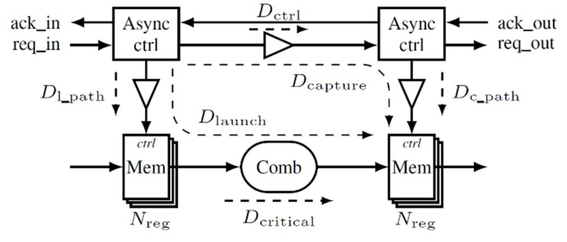
Micropipeline circuits (see Figure 1) have the advantage of keeping the same data path structure rather than a synchronous circuit, but without a global clock for synchronization. The control path, replacing the clock, is composed by small distributed controllers using a handshake protocol [19] and coordinates the data transfer. The request signal is delayed by Dctrl at least equal to the critical path Dcritical of the corresponding combinational block in order to guarantee the local timing assumption Equation (1). The delays Dl_path and Dc_path depend on the buffering required for the stage registers. When the number of registers, Nreg, increases, more buffers are needed. The following condition ensures the memorization of valid data:
DCapture > DLaunch
This approach intrinsically offers a set of delays, Dctrl, that can be used for spreading and controlling the emitted electromagnetic spectrum of a digital circuit. Deducted from Equation (1), Equation (2) provides the minimal value of Dctrl. The maximal value of Dctrl is only determined by the expected performances of the circuit.
Dctrl > Dl_path + Dcritical − Dc_path
In the following sections, we assume that the circuit architecture is kept and only the delay values are changed to control the electromagnetic spectrum. This guarantees that the method can be applied to any kind of micropipeline circuit.
4. Design Flow
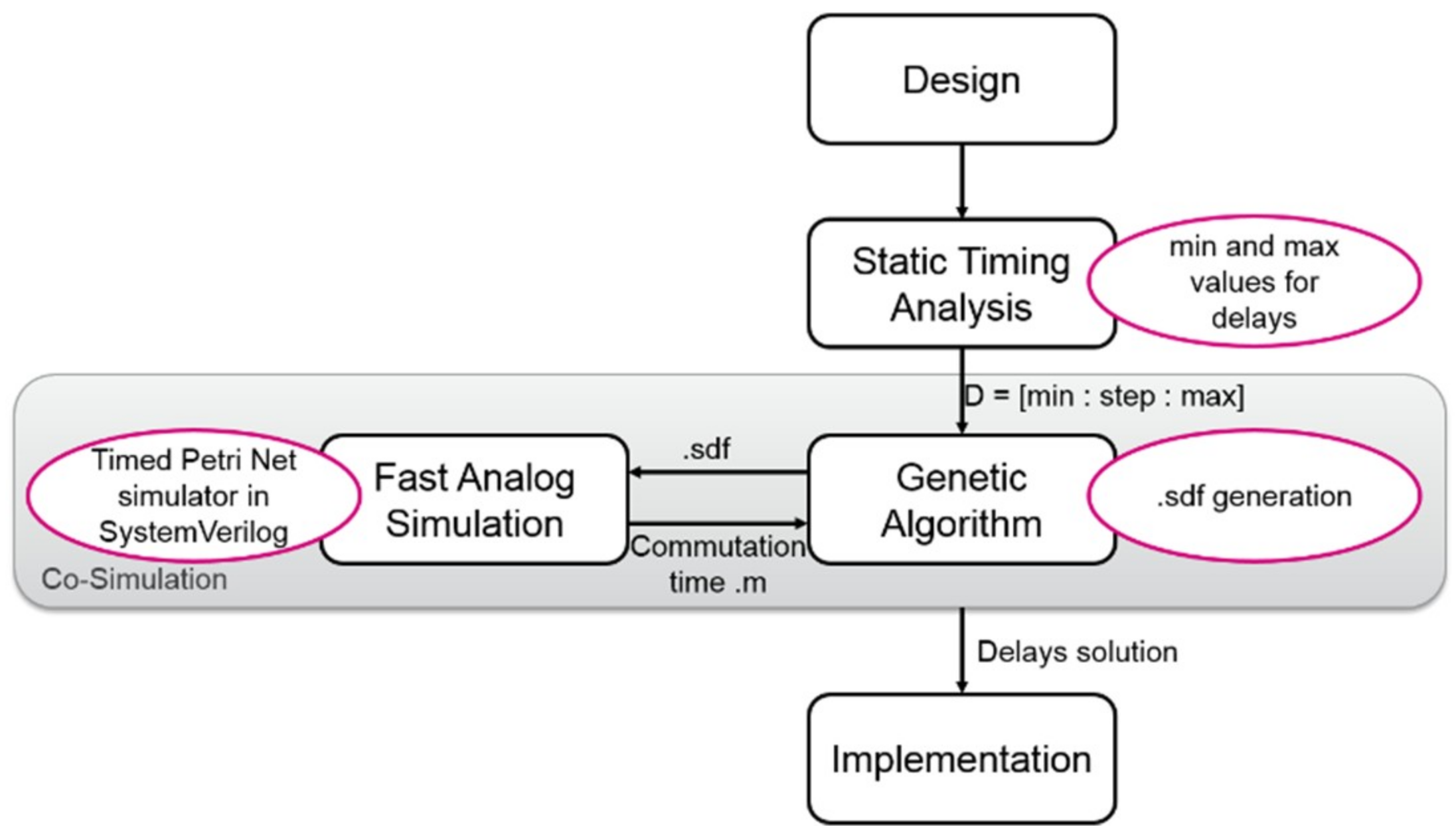
In order to shape the electromagnetic spectrum, a design flow is set up with a dedicated fast circuit simulator based on a Timed Petri Net model and behavioral current circuit estimation (see Figure 2). The first step consists of designing the circuit at Register Transfer Level (RTL). Then, a circuit timing analysis is performed where the delays Dctrl are extracted in order to determine the minimal value of these delays. The latter will be used as an absolute minimal reference when adjusting the delays for shaping the spectrum. Depending on the circuit targeted speed, a maximal value will also be fixed.
Next is the shaping step (the grey box in Figure 2). First, the Genetic Algorithm (GA) computes new delays Dctrl for each algorithm. Each combination is simulated with the Timed Petri Net simulator in order to obtain the current consumption curve. Then, the GA performs a Fast Fourier Transform on the current curve to compare the electromagnetic spectrum, with the spectral mask defined by the designer. A solution is found when a delay combination gives an electromagnetic spectrum that fits within the spectral mask. When the wished spectrum is obtained, the appropriated delays are inserted into the final circuit implementation.
4.1. Timing Extraction
A static timing analysis is performed to extract the critical path of each combinational stage, Dcritical. Then, the delays, Dl_path and Dc_path, are extracted depending on the number of buffers that have to be inserted between the asynchronous controllers and the registers. Finally, these values are injected in the Equation (2) in order to determine an appropriate value for Dctrl.
In order to quickly simulate the circuit current, a Timed Petri Net is created (as explained in the Section 5.1) to get the activation instants of each stage. With these instants, the circuit current consumption is computed with the asymmetric Laplace distribution current model defined in Section 5.2. This model basically describes the peaks produced by the registers and the combinational logic when activated by a local clock. Therefore, the number of registers per stage is also an important data source in order to weight the associated current peak when evaluating the stage current consumption.
4.2. Genetic Algorithm
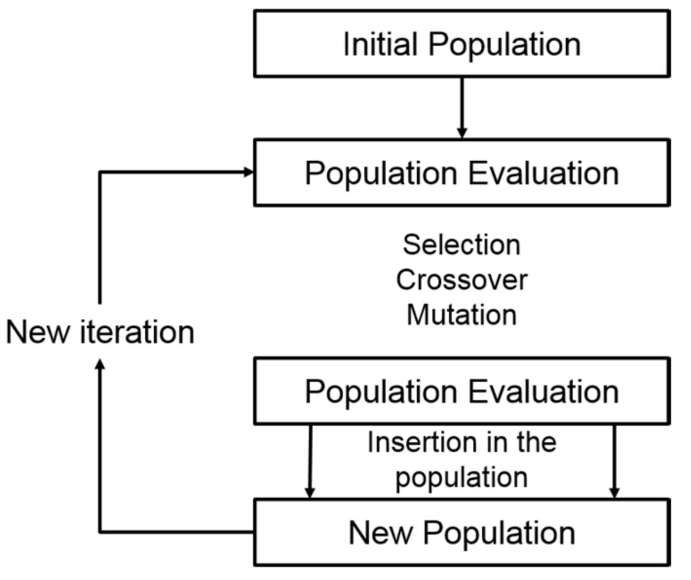
The current consumption curve is sent to the Genetic Algorithm (GA) in order to evaluate how far the spectrum is from fitting the mask [21]. Then, this algorithm, dedicated to optimization problems, is used to find the delays of the circuit to better match the specified spectral mask. It is necessary to use the genetic algorithm to find the delays of the circuit from the spectral mask because the mathematical problem is not a linear equation.
Introduced by the Professor Holland from the University of Michigan [22], the GA is inspired from the biology and natural phenomenon. This algorithm manipulates populations of individuals, where each one is a potential solution to the problem. Each individual is composed of genes that are the parameters of the problem. The GA process (see Figure 3) begins with an initial population composed of N individuals that are candidate solutions to the problem. Then, each individual x is associated to a cost evaluated with a fitness function f(x). After that, parents are selected to create the next generation in three steps.
First, in the current generation, the elite children, individuals with the best costs, are automatically selected for the next generation. As there is no guarantee that the children will be better than their parents, a proportion of the population is kept for the next generation. Then, like the reproduction in biology, the crossover children are created by the combination of two parents. Finally, mutant children resulting from random changes in the genes of the individuals are generated. This mutation step avoids being locked into a solution.
Finally, the new generation is evaluated with the fitness function. If a solution is found, the algorithm stops, otherwise it is repeated. To avoid the death of the population, all the generations must have the same size. This algorithm allows finding a solution to fit with the spectral mask but not to find “the best solution” (if we are able to define what “the best solution” is).
In our case, the genes are the stage delays. The algorithm begins with a random initial population of a hundred of individuals that respect minimum and maximum constraints for the genes. The GA fitness function performs a Fast Fourier Transform (FFT) of the current curve received from the fast current simulator to calculate the individual frequency spectrum. The frequency curve is then compared with the spectral mask defined by the designer. All of the spectral curve points, which are above the spectral mask, are added for computing the cost function of the individual. The GA stops when an individual with a cost function of 0 is found.
4.3. Co-Simulation between the Genetic Algorithm and the Timed Petri Net Model
The grey box of the Figure 2 shows the co-simulation step of the flow. The circuit Timed Petri Net is created and written in SystemVerilog, while the current evaluation and the genetic algorithm are implemented with Matlab. In order to find appropriate values for the micropipeline delays, an exchange of information between the Matlab software and the Timed Petri Net is required.
A feedback loop is then created between the Timed Petri Net, the Matlab current simulation, and the genetic algorithm to find a solution. Thanks to the current simulation, and by processing the current FFT (to get an image of current spectrum), the GA provides the Timed Petri Net with a new set of delays for the circuit. This is sent using an sdf (standard delay file) file containing all the timing information for the SystemVerilog model.
During the simulation of the Timed Petri Net, the activation instants of each register in the circuit are stored in a text file. Then, a Matlab function reads this file and produces the current curve. At each activation a current peak is associated due to the parameters obtained during the static timing analysis and the high level current modeling (see Section 5). Then, the Genetic Algorithm is started and its fitness function is called upon to evaluate the current curve. This is performed for each individual and for each generation of the genetic algorithm in order to find an individual with a spectrum fitting the spectral mask specified by the designer.
Once a solution is found with the co-simulation, the delays are generated by concatenating several elementary delays, and finally, then inserted in the circuit. The circuit implementation is thus ended and the final verification can be performed using the standard signoff flow.
5. High Level Current Modeling
5.1. Timed Petri Net Model
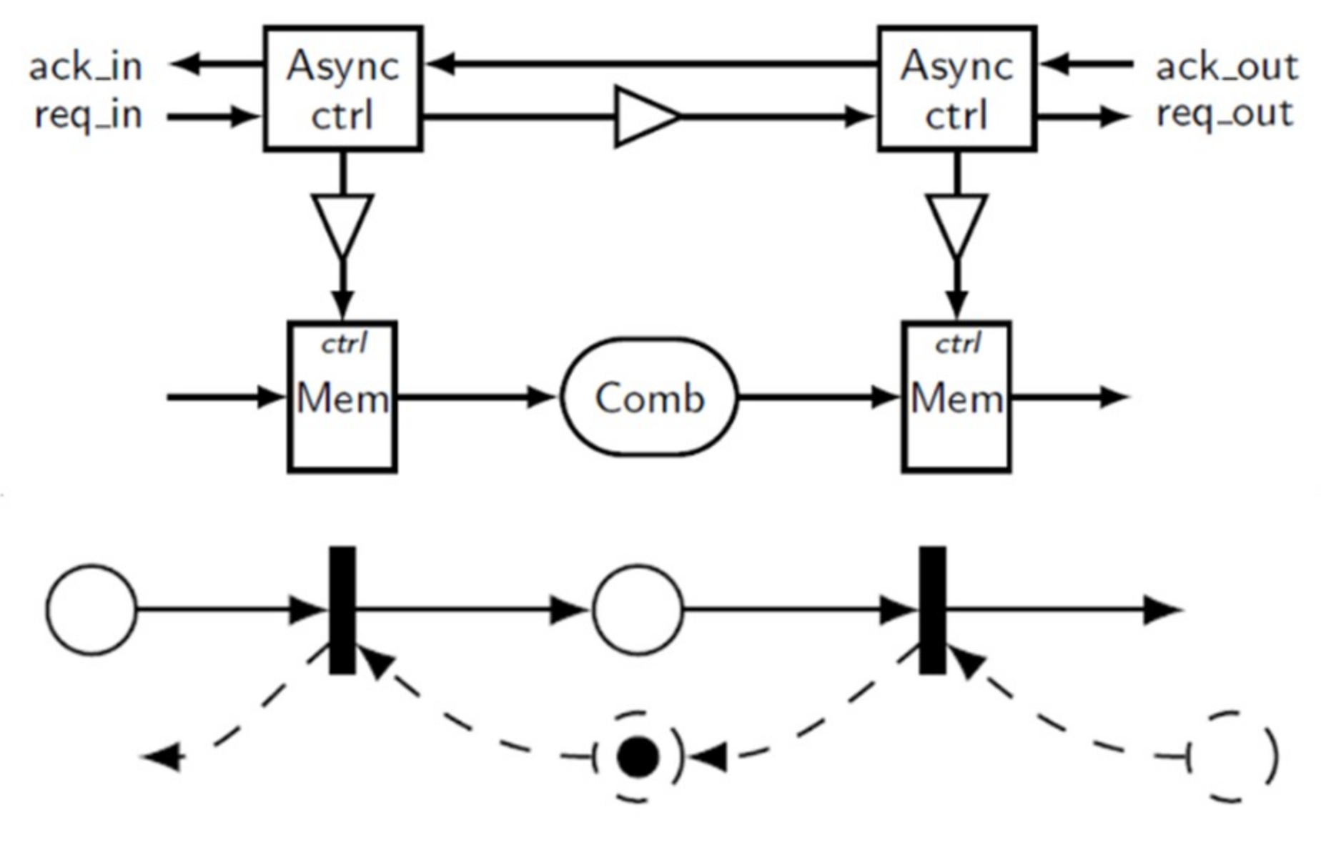
As the activity in an asynchronous circuit is concurrent, it can be modeled using a Timed Petri Net model. To simply and quickly evaluate the current consumption, current peaks are placed on the current waveform when the registers capture data. These captured times are evaluated thanks to the Timed Petri Net model.
This model is chosen because in the case of a non-linear micropipeline, with a merge or a split, for example, the functionality of the circuit has to be simulated in order to obtain the commutation times of the registers. Moreover, the objective of such a model is also able to help the designer to analyze the circuit control path; with this model, the designer is able to detect the deadlocks, and to check the liveliness of the controllers. Therefore, the Petri Nets are very helpful in designing the controllers in micropipeline circuits.
To construct the model, the designer extracts from its RTL description, or alternatively from a netlist, the communication channels corresponding to bundled-data stored in registers. The channels are modeled by a transition in our Timed Petri Net, while the combinational part or the delays in the controller are represented by a place (see Figure 4). Notice that not only the direct path (request) is depicted but also the feedback path with a dashed arrow (acknowledgement). This will be later useful for interpreting the protocol impact on the circuit behavior when the Timed Petri Net model will be enriched in its SystemVerilog description. The approach can be generalized by considering communication channels, like joins, forks, splits, and merges when the pipeline structure is no longer linear [23].
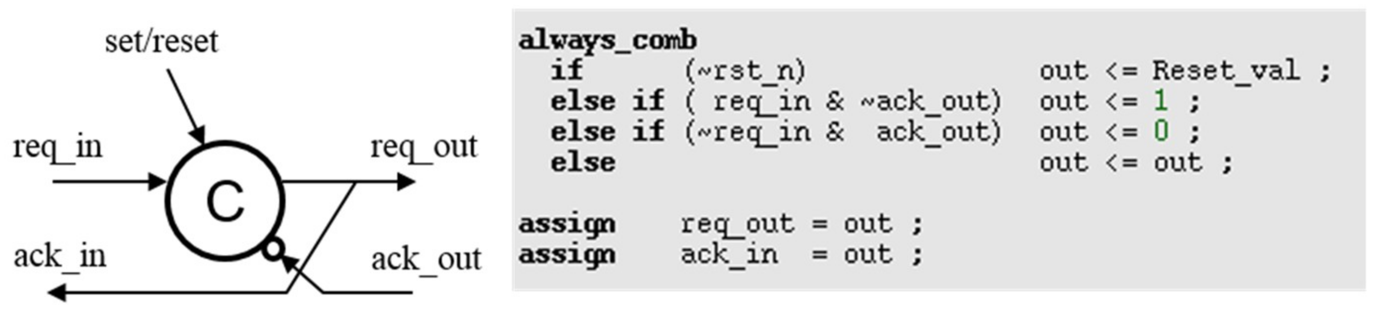
In our method, the Timed Petri Net model is described in SystemVerilog. This choice has been made because SystemVerilog uses an event-based simulator, and thus, allows the Timed Petri Net simulation. Figure 5 gives an example representing the Timed Petri Net enrichment by replacing the classical transition rules with a communication protocol. The behavior of the Timed Petri Net transition is substituted by the behavior of a controller also described in SystemVerilog. The given description represents a 4-phase Weak Condition Half Buffer protocol, but other protocols can be tested by modifying the SystemVerilog code.
The transitions in the Timed Petri Net model represent the controllers, which synchronize the circuit. The place represents the delay between two controllers and the timing arc in the gates of the circuit.
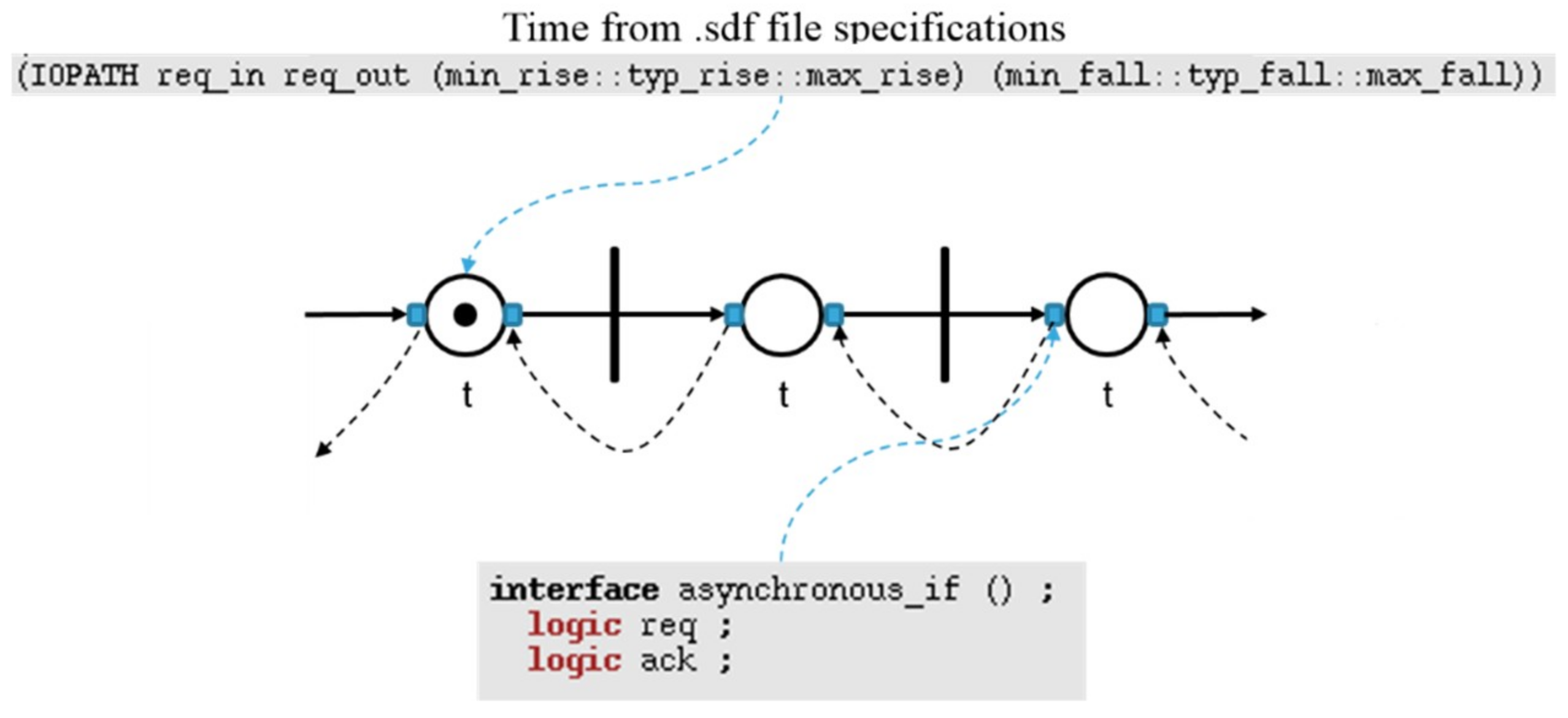
An example of our Timed Petri Net model is given in Figure 6. To summarize, the circles represent the timed places. The bars represent the transitions allowing the synchronization between two places. Finally, the arcs represent the bundled-data channels, with the request signal (solid arc) and the acknowledgment signal (dashed arc). The connections between the places and the arcs are made with SystemVerilog interfaces. The timings stored within the places are coming from a standard delay file (.sdf), which contains all the delays of the control path. A transition fires if the three following conditions are met:
- All the inputs of the transition must have at least one token;
- The time specified in its input places has already expired;
- All the outputs of the transition must be token-free.
When a transition fires, one token is removed from each input and one token is placed at each output.
Each block of the Timed Petri Net is described in SystemVerilog, as the controller in Figure 5. Then, they are connected with the request and the acknowledgment signals that are integrated in a SystemVerilog interface. This generic interface allows the user to easily connect the different blocks. Moreover, if the designer wishes to evaluate several communication protocols, the only blocks to change are the controller blocks, while the connections still remain the same.
Thanks to the SystemVerilog test bench, the activation instants of the registers are computed and memorized in a file. A current pulse is then associated at each activation time to obtain the total current consumption of the micropipeline circuit.
5.2. Current Estimation
In synchronous circuits, the current consumption can be modelled based on the following considerations:
- In CMOS circuits, the gate switching produces the current consumption.
- Most of the gate switching activity is localized in time just after the clock edges.
- The clock switching activity of the flip-flops and the clock tree produce an important part of the current consumption.
For that reason, the peaks are uniformly distributed in time and generate harmonics strongly impacting the electromagnetic spectrum.
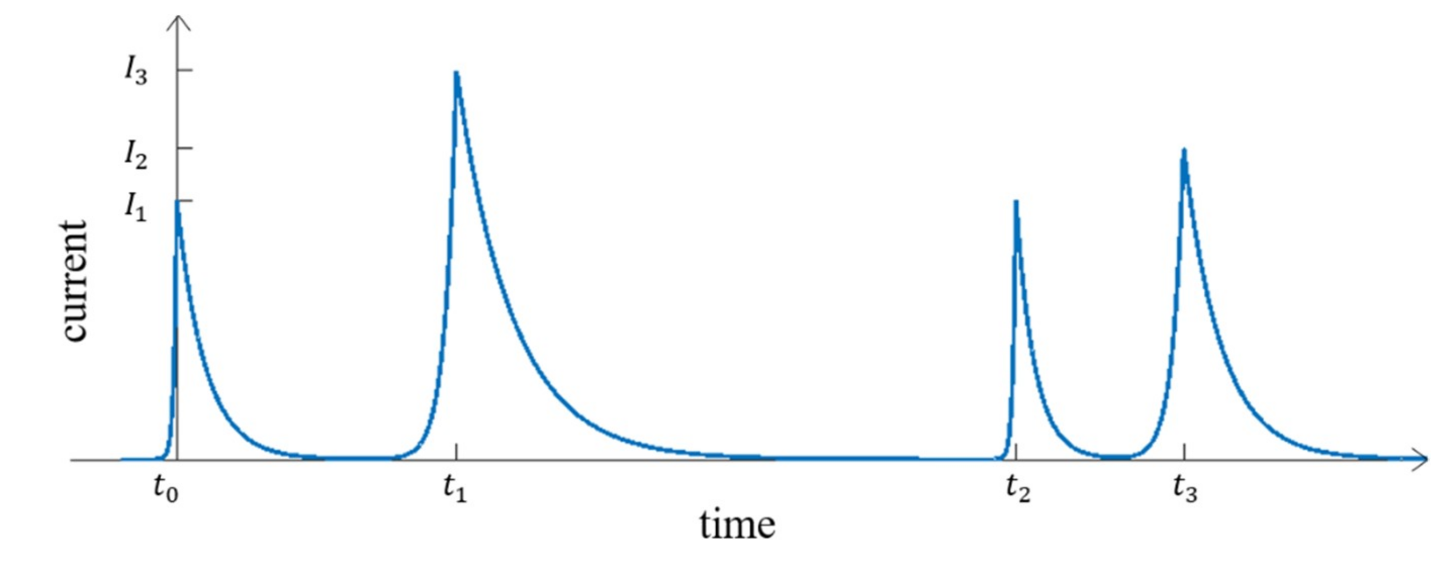
Therefore, the consumption of a digital CMOS circuit can simply be modeled thanks to current pulses (see Figure 7).
As the global clock is removed in asynchronous circuits, the flip-flop switching activity is now driven by local asynchronous controllers, with a similar shape. Consequently, the peak distribution is no longer uniform and this helps to reduce the harmonics.
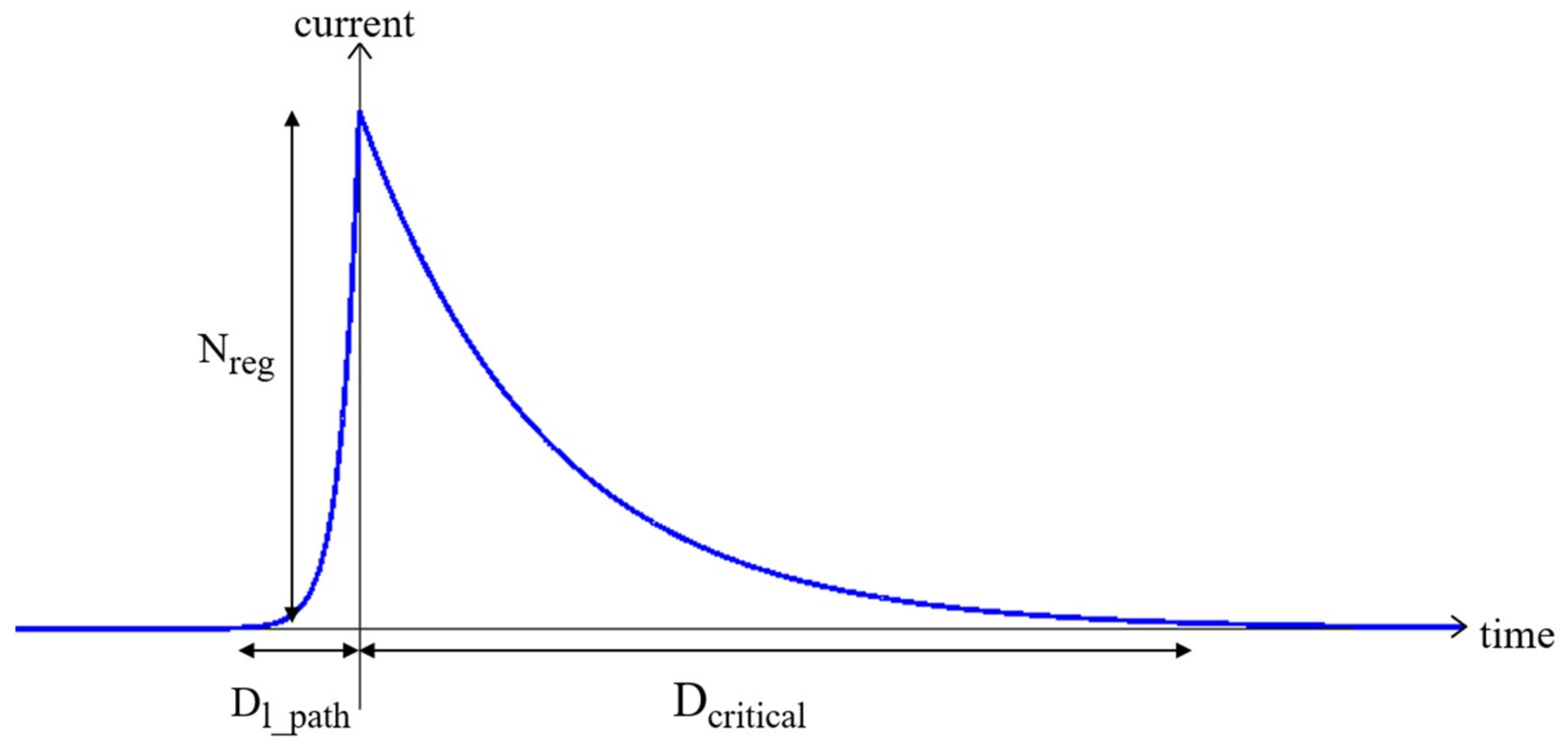
In the present method, the asymmetric Laplace distribution is used to model a current pulse, as shown in Figure 8. This distribution is composed of two exponentials of unequal scale back-to-back. Nevertheless, it is also possible to simply model the current peak using a triangle.
The time constants of the current peaks are determined for each stage using the extracted delay of the circuit during the timing analysis. The rise time of the first exponential is equal to the delay from the controller to the registers, represented by Dl_path in Figure 1 and Figure 8. This time depends on the number of registers Nreg that are driven by the controller. Indeed, the length of the request signal tree between the controller and the registers depends on Nreg. This number also determines the height of the peak. The maximum of the consumption occurs when all of the stage sample data are registered. The consumption for the memorization of one register is determined thanks to the datasheet of the library or with a spice simulation. Then, these values are multiplied by the number of the registers in the stage, Nreg. The higher the peak, the longer the rise time of the exponential. This is a worst case scenario, as we are considering that all registers are toggling.
The second exponential represents the consumption of the combinational logic after the registers. The fall time of this exponential is the delay of the stage critical path, represented by Dcritical.
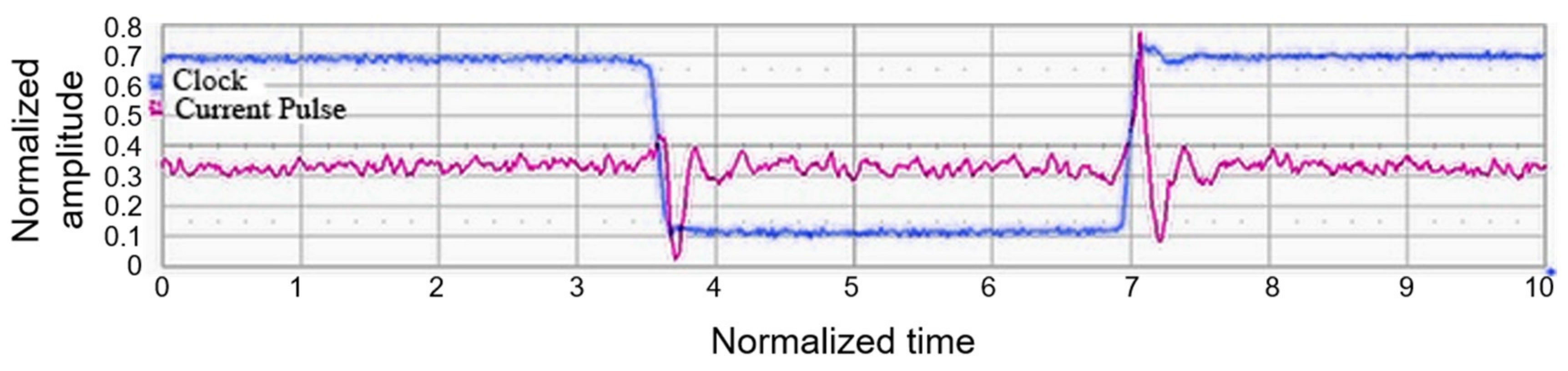
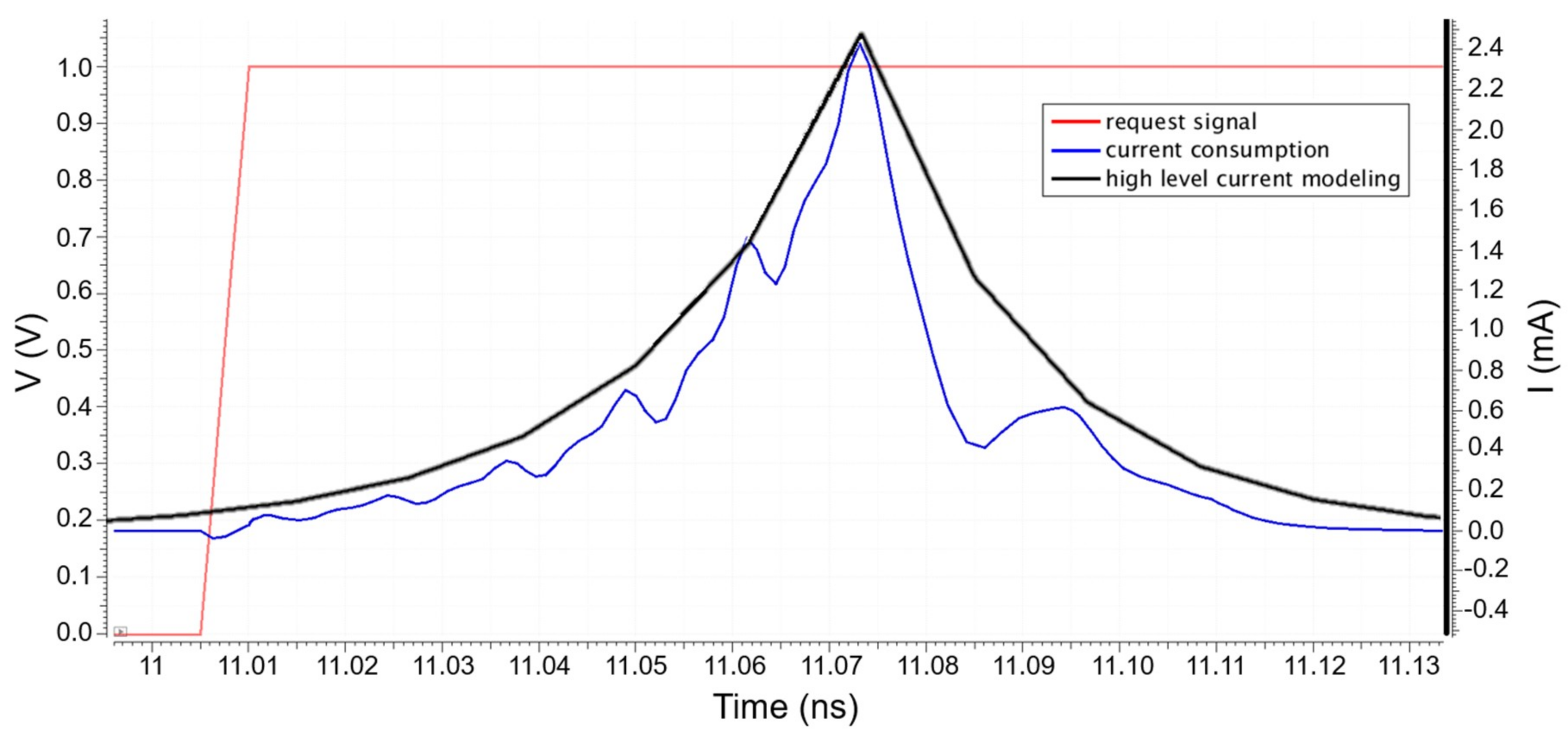
Thanks to these two exponentials, as current peaks model the registers and the logic cone consumptions, the current model is quite realistic. To justify the relevance of the asymmetric Laplace distribution model, one stage of registers, with a clock tree and a simple combinational part, has been simulated with Cadence Spectre®. The blue curve of Figure 9 represents the current consumption of this stage after the rising edge of the request signal (the red signal). The current consumption curve of Figure 9 can be assimilated to an asymmetric Laplace distribution.
The model of the current consumption of the circuit is obtained by associating the Timed Petri Net model and the current peak model. A peak, with its parameters, is placed on each firing instant computed by the Timed Petri Net model. Figure 10 represents the model of the current consumption of a 4-stage micropipeline. At each firing instant, a current peak occurs. Their different heights correspond to the various numbers of registers for each stage. As there are different peak heights for the current, the rise and fall times become longer when the current peaks increase.
Due to the static timing analysis, the Timed Petri Net, and the asymmetric Laplace distribution modeling of the current peak, a high level current model is obtained. This model makes enables the fast current simulation of a micropipeline circuit, allowing the genetic algorithm to efficiently evaluate a set of appropriated delays for shaping the electromagnetic emissions.
To take into account the process variations, two strategies are conceivable. First, the analysis of the circuit can be done for different corners. In this case, a set of delays is found for each corner. Then, thanks to programmable delay lines, it is possible to program the set of delays corresponding to the corner of the fabricated chip. The second solution is to perform the analysis with the worst (slower) corner. A set of delays is then found matching the spectral mask. Then, if the fabricated chip has a better corner, it is always possible to add complementary delays with the programmable delay lines in order to retrieve the original delays of the slowest corner.
6. Simulation Results
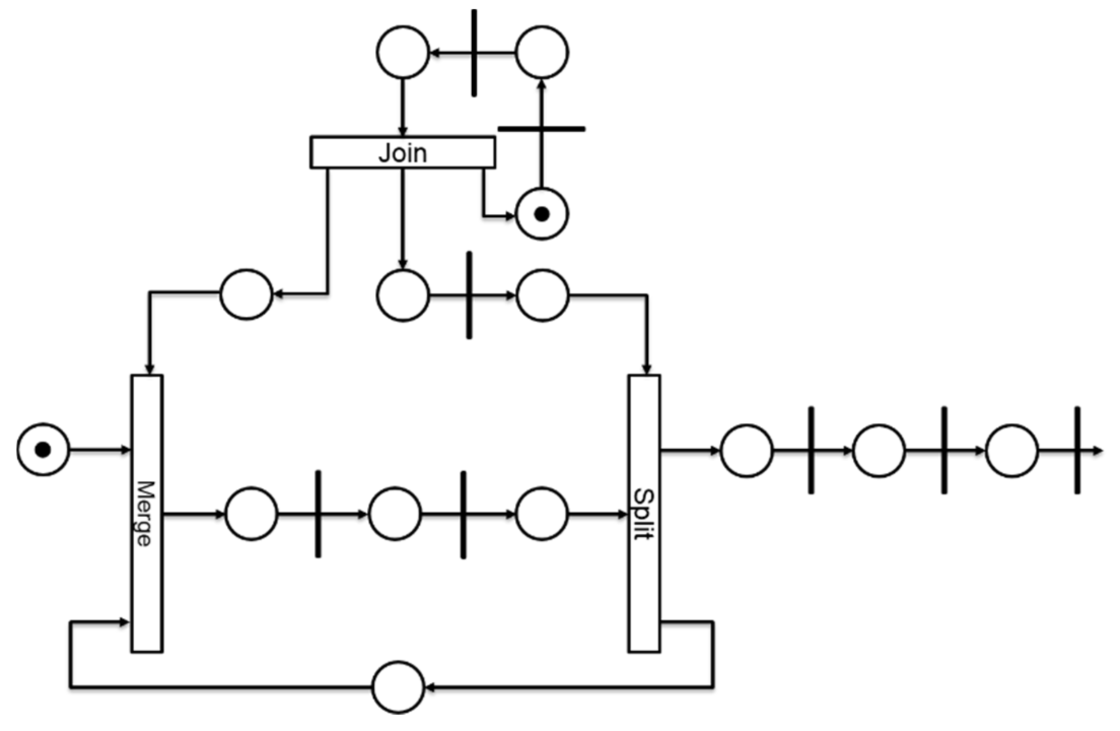
An Advanced Encryption Standard (AES) has been designed in micropipeline style with the proposed flow in order to shape its electromagnetic spectrum. Figure 11 shows the Timed Petri Net model of the AES. For the sake of clarity, the acknowledgment arcs are not represented. The bars represent the controllers, here with a 4-phase protocol. The arcs represent the request signals. The circles represent the delays. In the AES model, a merge and a split structure have been used for the data selection and a join for the synchronization with the counter.
The first step of our flow is to design the circuit at RTL level. Here, the micropipeline AES is designed in VHDL and the data path is synthesized with standard EDA tools. Next, a static timing analysis is performed to extract the minimal values of the delays and the parameters required for modeling the current pulses. Then these parameters are used in Matlab to initialize the genetic algorithm. In parallel, the behavior of each controller block is described in SystemVerilog. The controllers are connected together in order to create the Timed Petri Net like in Figure 11. The co-simulation between the genetic algorithm and the Timed Petri Net is performed to find a solution fitting with the spectral requirements. Once the spectrum of an individual is under the spectral mask, the number of buffers needed for each stage is deduced from the solution. Finally, the micropipeline AES is implemented by associating the synthesized data path, the controllers, and the delays.
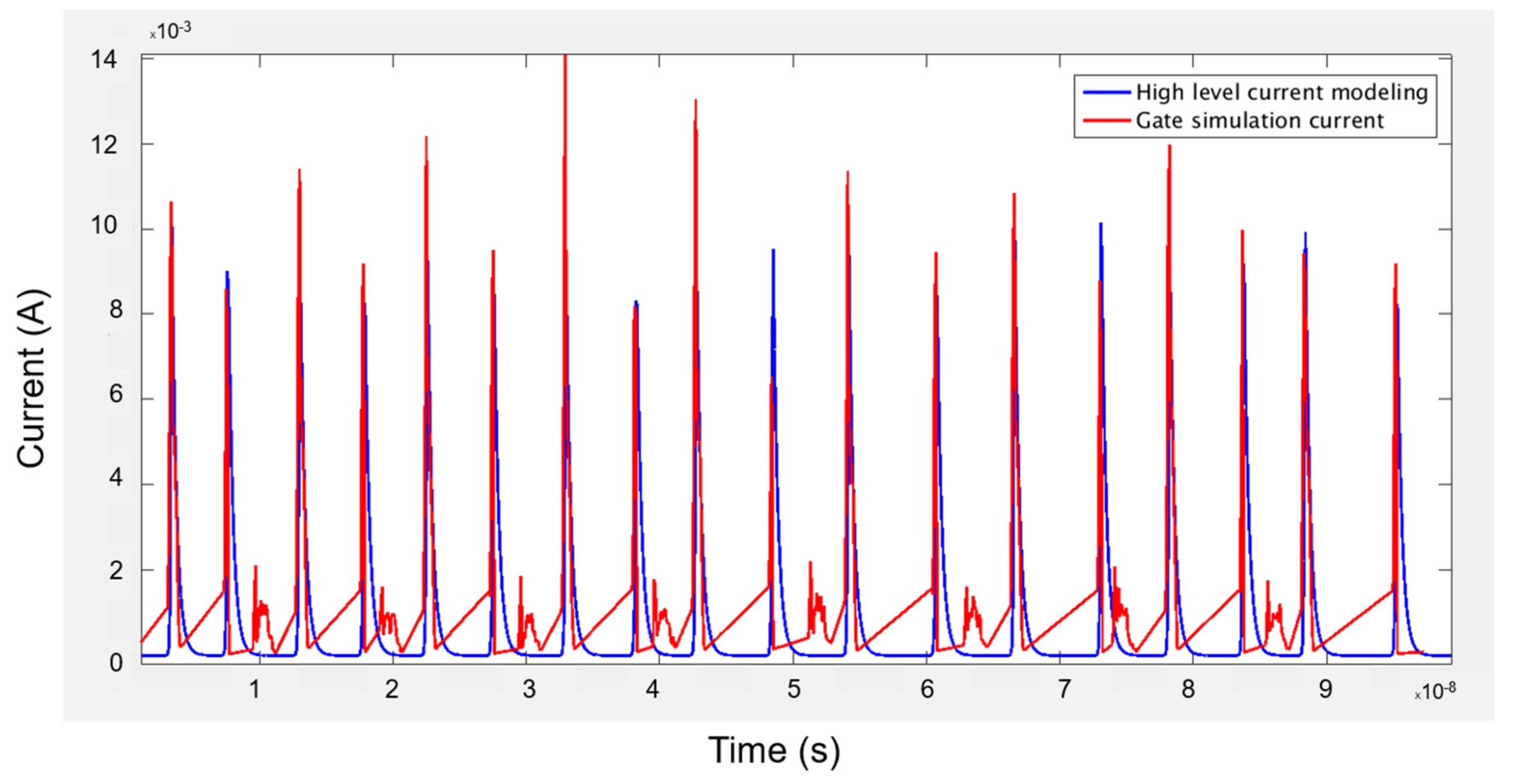
For clarity, in Figure 12 (too many peaks for the full AES), the evaluation, thanks to our fast simulator based on our high-level current model, is performed only using the second stage of the AES. The obtained current curve is compared to a current curve obtained with a gate simulation. Figure 12 shows both current curves: in blue, the current simulated with our high-level modeling, and in red, the current curve resulting from the gate simulation. We observe that the activation times are the same on both curves. Figure 12 shows that the height of the current peaks is not always exactly the same. For the high level current modeling curve, the first cause is the time step of the graph x-axis, which is too rough (100 ps) to always include the highest point of the peaks. The other reason comes from the gate simulation, where the register current consumption also depends on the data values at their inputs. Memorizing a “one” is more consuming than memorizing a “zero”. The simulation curves of the second stage include eighteen current peaks corresponding to the nine AES loops. Indeed, the rise and the fall edges are considered.
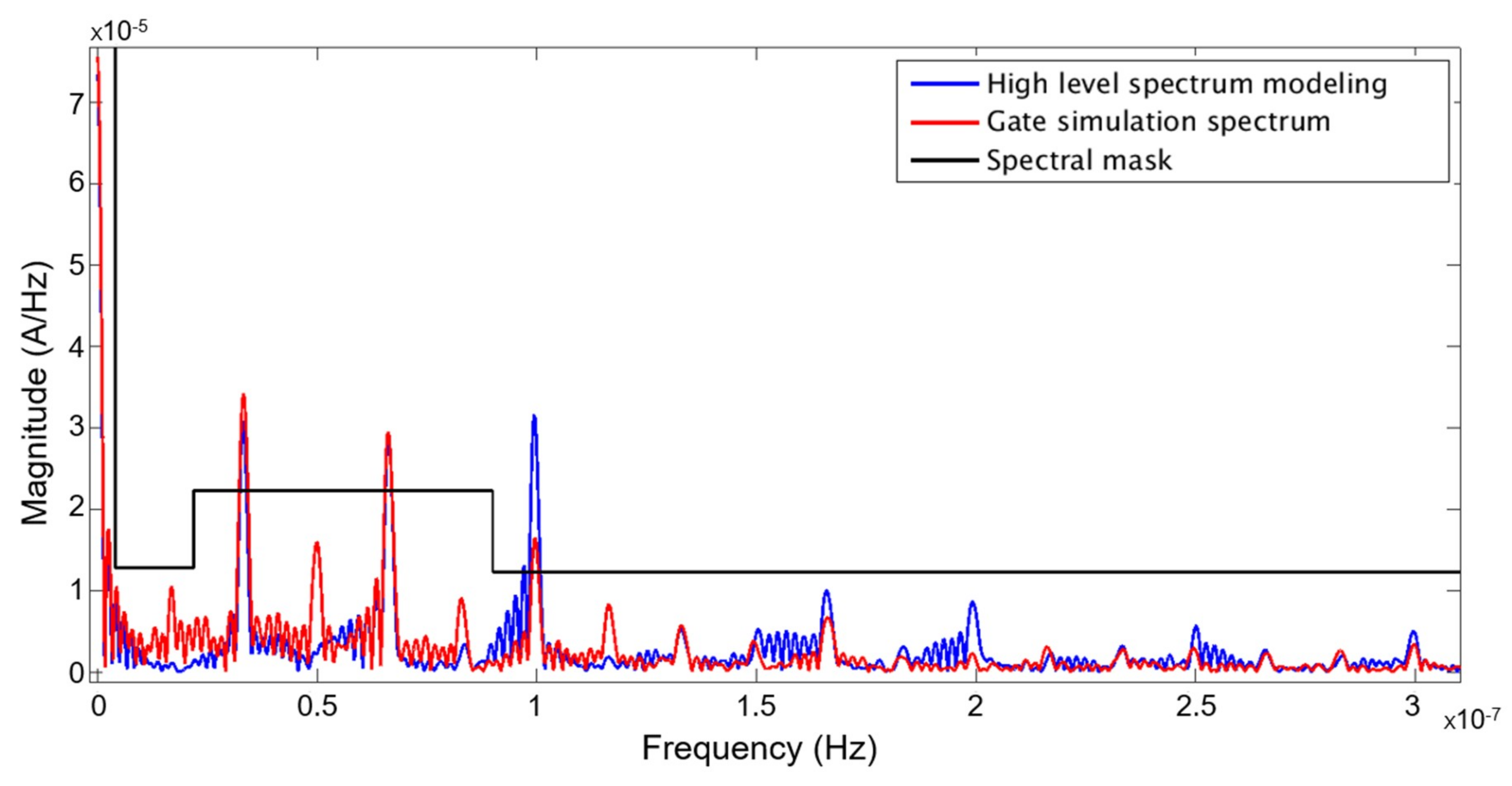
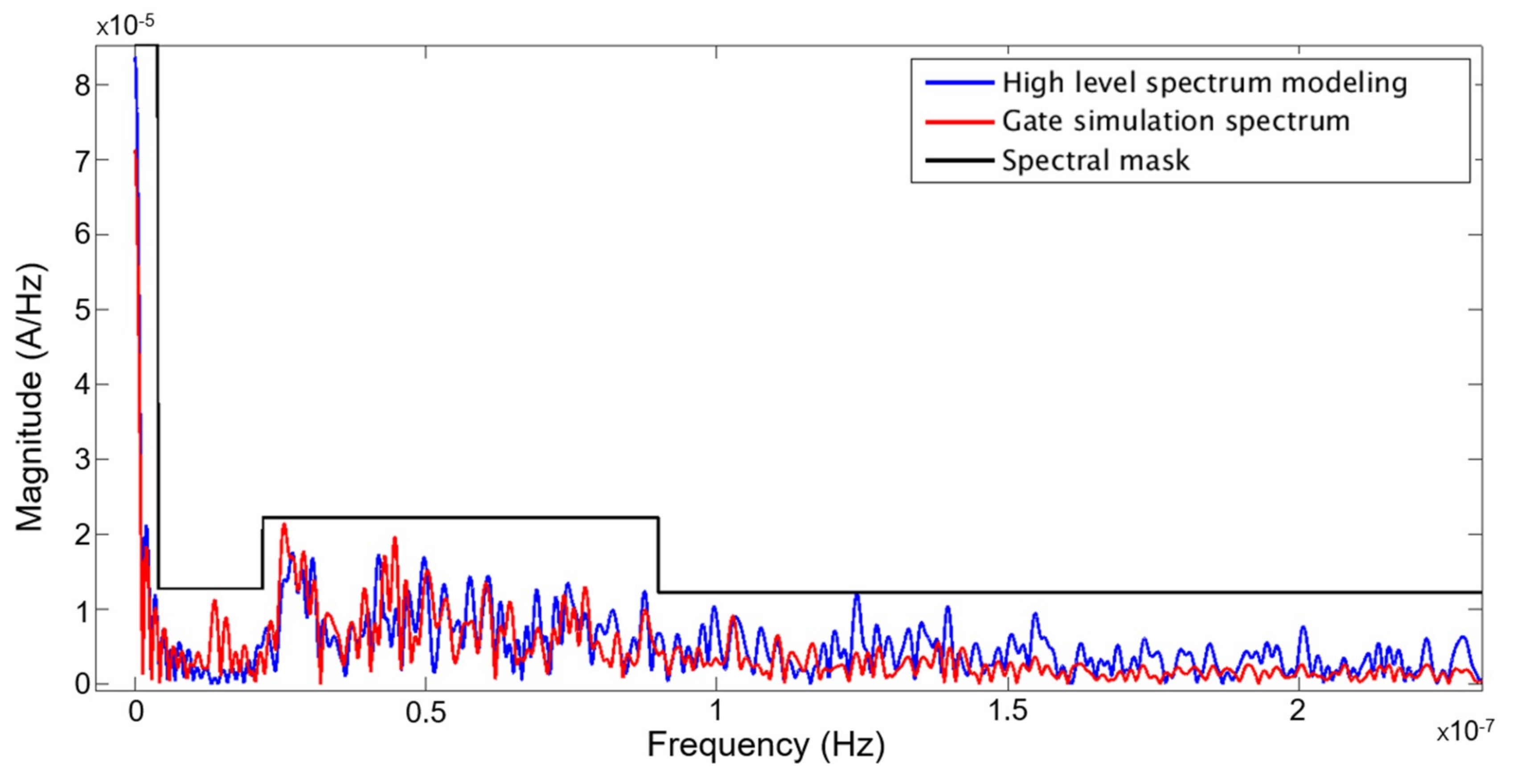
At the beginning of the shaping process, Figure 13 is obtained by applying a FFT on the current curve of the entire AES, not only on the current curve of Figure 12 (representing the second stage). The spectrum of the gate simulation, the blue curve, is compared with the spectrum of the co-simulation, the red curve. We observe that the high level model spectrum is more pessimistic than the gate simulation spectrum. The black curve represents the spectral mask chosen for this analysis. The main idea is to first reduce the harmonics. Indeed, we can see that the current spectrum is above the mask, so it does not fit with the mask specifications.
In Figure 14, the high level spectrum modeling of the entire AES is compared to the gate simulation spectrum after applying our design flow (described in Section 4). The set of delays fitting the spectral mask has been found thanks to the genetic algorithm after approximately six hours.
We observe that both spectrums (the high level model spectrum in blue and the gate simulation spectrum in red) are always below the spectral mask (black curve). We note that the gate simulation spectrum is generally under the high level spectrum modeling in both Figure 13 and 14. Our model does not consider the parasitic effects that occur during the switching of the combinational logic, like glitches or cross-talk [24] (the small peaks in Figure 12). These effects contribute to spreading the spectrum of the circuit. As our model does not yet take into account these effects, our current curve is a little bit pessimistic compared to that of the gate simulation.
7. Conclusions
This paper presents high level current modeling for fast simulations and the first design flow for shaping and controlling the electromagnetic spectrum of an integrated circuit. With such a design flow, the designer is able to implement a micropipeline circuit fitting a spectral mask, thanks to an appropriate set of delays. The use of micropipeline circuits allows quick building of a Timed Petri Net model for simulation of the temporal behavior of the control part. This Timed Petri Net model helps to find the deadlocks and to guarantee the liveliness of the circuit. Of course, it also determines the activation instants of all the circuit stages. Moreover, it can be used to evaluate solutions with different communication protocols. The extraction of the register capture times allows a fast current circuit simulation thanks to a high level current model based on asymmetric Laplace distributions modeling the current peaks. The heights, the path delays, and the rise and fall times of the peaks are determined thanks to the data used and produced by the static timing analysis tools. The genetic algorithm reevaluates the current curve corresponding to a set of delays at each new generation until a solution fitting within the spectral mask is found. A co-simulation backbone is used between the Timed Petri Net described in SystemVerilog, the Matlab current simulation, and the genetic algorithm. This way, the genetic algorithm exchanges the delays with the Timed Petri Net model, and the latter sends it back to the activation instants required for modeling the circuit current. Once a solution is found, the circuit can be implemented by adding the generated controllers to the synthesized data path with the right delay values.
This design flow has been evaluated on an Advanced Encryption Standard (AES) designed in micropipeline. The comparison between the curves obtained with our design flow and the curves obtained with the gate-level simulations has been made. It shows that the activation instants of both curves are the same. Then, we compare the frequency spectrum extracted from the co-simulation and from the gate simulation. It shows that after applying the genetic algorithm optimization, both spectrums fit with the spectral mask defined by the designer. Notice that as our model does not take into account the parasitic effects that occur during the switching of the combinational logic, our estimation is a little bit pessimistic, especially in the high-frequency range. A test chip has already been taped-out and the next step will be the validation of our method and design flow with real measurements.
Author Contributions
Supervision, S.E. and L.F.; writing—original draft, S.G.; writing—review and editing, S.E. and L.F.
Funding
This work has been partially supported by the Labex PERSYVAL-lab (ANR-11-LABX-0025-01) and the ANRT (Convention Cifre No. 2016/0718).
Conflicts of Interest
The authors declare no conflict of interest.
References
- Hung, C.M.; Muhammad, K. RF/Analog and Digital Faceoff-Friends or Enemies in an RF SoC. In Proceedings of the 2010 International Symposium on VLSI Technology Systems and Applications (VLSI-TSA), Hsin Chu, Taiwan, 26–28 April 2010; pp. 19–20. [Google Scholar]
- Cazzaniga, M.; Doriol, P.J.; Sanna, A.; Blanc, E.; Liberali, V.; Pandini, D. Evaluating the impact of substrate noise on conducted EMI in automotive microcontrollers. In Proceedings of the 9th International Workshop on,Electromagnetic Compatibility of Integrated Circuits (EMC Compo), Nara, Japan, 15–18 December 2013; pp. 129–133. [Google Scholar]
- Ramdani, M.; Sicard, E.; Boyer, A.; Dhia, S.B.; Whalen, J.J.; Hubing, T.H.; Coenen, M.; Wada, O. The Electromagnetic Compatibility of Integrated Circuits—Past, Present, and Future. IEEE Trans. Electromagn. Compat. 2009, 51, 78–100. [Google Scholar] [CrossRef] [Green Version]
- Rossi, R.; Torelli, G.; Liberali, V. Model and verification of triple-well shielding on substrate noise in mixed-signal CMOS ICs. In Proceedings of the ESSCIRC 2004—29th European Solid-State Circuits Conference (IEEE Cat. No.03EX705), Estoril, Portugal, 16–18 September 2003; pp. 643–646. [Google Scholar]
- Schneider, M.J. Design Considerations to Reduce Conducted and Radiated EMI. Master’s Thesis, Purdue University, West Lafayette, IN, USA, April 2010. [Google Scholar]
- Mardiguian, M. Controlling Radiated Emissions by Design, 3rd ed.; Kluwer Academic Publishers: Norwell, Massachusetts, 2014. [Google Scholar]
- Steinecke, T. Design-in for EMC on CMOS large-scale integrated circuits. In Proceedings of the IEEE EMC International Symposium Electromagnetic Compatibility, Montreal, QC, Canada, 13–17 August 2001; pp. 910–915. [Google Scholar]
- Hardin, K.B.; Fessler, J.T.; Bush, D.R. Spread spectrum clock generation for the reduction of radiated emissions. In Proceedings of the IEEE Symposium on Electromagnetic Compatibility, Sendai, Japan, 27–29 September 1994; pp. 227–231. [Google Scholar]
- Fan, X.; Schrape, O.; Marinkovic, M.; Dahnert, P.; Krstic, M.; Grass, E. GALS Design for Spectral Peak Attenuation of Switching Current. In Proceedings of the IEEE 19th International Symposium on Asynchronous Circuits and Systems, Santa Monica, CA, USA, 19–22 May 2013; pp. 83–90. [Google Scholar]
- Fan, X.; Stegmann, M.B.; Schrape, O.; Zeidler, S.; Jensen, I.G.; Thorsen, J.; Bjerregaard, T.; Krstić, M. Frequency-Domain Optimization of Digital Switching Noise Based on Clock Scheduling. IEEE Trans. Circuits Syst. Regul. Pap. 2016, 63, 982–993. [Google Scholar] [CrossRef]
- Stegmann, G.; Gloor, D.; Baumann, D.; Peeters, A.; van Berkel, K.; van Gageldonk, H. An asynchronous low-power 80C51 microcontroller. In Proceedings of the 1998 Fourth International Symposium on Advanced Research in Asynchronous Circuits and Systems, San Diego, CA, USA, 30 March–2 April 1998; pp. 96–107. [Google Scholar]
- Berkel, K.V.; Josephs, M.B.; Nowick, S.M. Scanning the technology: Applications of asynchronous circuits. Proc IEEE 1999, 223–233. [Google Scholar]
- de Cristo, R.A.L.; Jasinski, R.P.; Pedroni, V.A. Analysis and Preliminary Measurements of Radiated Emissions in an Asynchronous Circuit versus its Synchronous Counterpart. In Proceedings of the International Conference on Reconfigurable Computing and FPGAs, Cancun, Mexico, 13–15 December 2010; pp. 127–131. [Google Scholar]
- Furber, S.B.; Garside, J.D.; Riocreux, P.; Temple, S.; Day, P.; Liu, J.; Paver, N.C. AMULET2e: An asynchronous embedded controller. Proc. IEEE 1999, 87, 243–256. [Google Scholar] [CrossRef]
- Bouesse, G.F.; Ninon, N.; Sicard, G.; Renaudin, M.; Boyer, A.; Sicard, E. Asynchronous logic VS Synchronous logic: Concrete results on electromagnetic emissions and conducted susceptibility. In Proceedings of the 6th International Workshop on Electromagnetic Compatibility of Integrated Circuits, Torino, Italy, 28–30 November 2007; pp. 99–102. [Google Scholar]
- Panyasak, D.; Sicard, G.; Renaudin, M. A current shaping methodology for lowering EM disturbances in asynchronous circuits. Microelectron. J. 2004, 35, 531–540. [Google Scholar] [CrossRef]
- Lee, J.G. A Low EMI Circuit Design with Asynchronous Multi-Frequency Clocking. IEICE Trans. Electron. 2014, 97, 1158–1161. [Google Scholar] [CrossRef]
- Federal Communication Commission. First Report and Order In the Matter of Revision of the Commission’s Rules Regarding Ultra-Wideband Transmission Systems; ET Docket 98-153, FCC 02-48; Federal Communication Commission: Washington, DC, USA, 2002.
- Sutherland, I.E. Micropipelines. Commun. ACM 1989, 32, 720–738. [Google Scholar] [CrossRef] [Green Version]
- Sparsø, J.; Furber, S. Principles of Asynchronous Circuit Design: A Systems Perspective; Kluwer: Boston, MA, USA, 2010. [Google Scholar]
- Germain, S.; Engels, S.; Fesquet, L. Event-based design strategy for circuit electromagnetic compatibility. In Proceedings of the 3rd International Conference on Event-Based Control, Communication and Signal Processing (EBCCSP), Madeira, Portugal, 24–26 May 2017; pp. 1–7. [Google Scholar]
- Holland, J.H. Adaptation in Natural and Artificial Systems: An Introductory Analysis with Applications to Biology, Control, and Artificial Intelligence; University of Michigan Press: Ann Arbor, MI, USA, 1975. [Google Scholar]
- Simatic, J.; Cherkaoui, A.; Bertrand, F.; Bastos, R.P.; Fesquet, L. A Practical Framework for Specification, Verification, and Design of Self-Timed Pipelines. In Proceedings of the 23rd IEEE International Symposium on Asynchronous Circuits and Systems (ASYNC), San Diego, CA, USA, 21–24 May 2017; pp. 65–72. [Google Scholar]
- Monteiro, J.; Devadas, S.; Ghosh, A.; Keutzer, K.; White, J. Estimation of average switching activity in combinational logic circuits using symbolic simulation. IEEE Trans. Comput. Aided Des. Integr. Circuits Syst. 1997, 16, 121–127. [Google Scholar] [CrossRef] [Green Version]
Figure 1.
Architecture of a micropipeline circuit—the request signal indicates valid data and the acknowledgment signal notify that the register is ready to receive new data.
Figure 1.
Architecture of a micropipeline circuit—the request signal indicates valid data and the acknowledgment signal notify that the register is ready to receive new data.

Figure 2.
Design flow to control the electromagnetic emissions.

Figure 3.
Genetic algorithm process.

Figure 4.
The micropipeline circuit and its model.

Figure 5.
Representation of a micropipeline controller and its description in SystemVerilog with the 4-phase Weak Condition Half Buffer protocol.
Figure 5.
Representation of a micropipeline controller and its description in SystemVerilog with the 4-phase Weak Condition Half Buffer protocol.

Figure 6.
Representation of the Timed Petri Net, with an example of a time specification in the .sdf file and the interface of the place with the channel composed of the request and acknowledgment signals.
Figure 6.
Representation of the Timed Petri Net, with an example of a time specification in the .sdf file and the interface of the place with the channel composed of the request and acknowledgment signals.

Figure 7.
CMOS current consumption with peaks on clock edges.

Figure 8.
Shape of a current pulse using the asymmetric Laplace distribution model.

Figure 9.
Spectre® simulation of one stage of registers with its clock tree and a simple combinational part. The red curve represents the event on the clock tree and the blue curve represents the current consumption.
Figure 9.
Spectre® simulation of one stage of registers with its clock tree and a simple combinational part. The red curve represents the event on the clock tree and the blue curve represents the current consumption.

Figure 10.
Shape of the total current consumption in time for a 4-stage micropipeline.

Figure 11.
Timed Petri Net model representation of the micropipeline. Advanced Encryption Standard, with the controllers (bars), the request signals (arcs), the delays (circles), and the merge, split, and join blocks.
Figure 11.
Timed Petri Net model representation of the micropipeline. Advanced Encryption Standard, with the controllers (bars), the request signals (arcs), the delays (circles), and the merge, split, and join blocks.

Figure 12.
Current curve, for the second stage of the Advanced Encryption Standard (AES), obtained with the co-simulation in blue and with the gate simulation in red.
Figure 12.
Current curve, for the second stage of the Advanced Encryption Standard (AES), obtained with the co-simulation in blue and with the gate simulation in red.

Figure 13.
Spectrum of the AES obtained with the co-simulation (blue curve) and with the gate simulation (red curve). The black curve corresponds to the spectral mask defined by the designer.
Figure 13.
Spectrum of the AES obtained with the co-simulation (blue curve) and with the gate simulation (red curve). The black curve corresponds to the spectral mask defined by the designer.

Figure 14.
Spectrum of the AES obtained with the co-simulation (blue curve) and with the gate simulation (red curve) after applying the genetic algorithm optimization. The black curve corresponds to the spectral mask defined by the designer.
Figure 14.
Spectrum of the AES obtained with the co-simulation (blue curve) and with the gate simulation (red curve) after applying the genetic algorithm optimization. The black curve corresponds to the spectral mask defined by the designer.

© 2019 by the authors. Licensee MDPI, Basel, Switzerland. This article is an open access article distributed under the terms and conditions of the Creative Commons Attribution (CC BY) license (http://creativecommons.org/licenses/by/4.0/).
Share and Cite
MDPI and ACS Style
Germain, S.; Engels, S.; Fesquet, L. High Level Current Modeling for Shaping Electromagnetic Emissions in Micropipeline Circuits. J. Low Power Electron. Appl. 2019, 9, 6. https://doi.org/10.3390/jlpea9010006
AMA Style
Germain S, Engels S, Fesquet L. High Level Current Modeling for Shaping Electromagnetic Emissions in Micropipeline Circuits. Journal of Low Power Electronics and Applications. 2019; 9(1):6. https://doi.org/10.3390/jlpea9010006
Chicago/Turabian StyleGermain, Sophie, Sylvain Engels, and Laurent Fesquet. 2019. "High Level Current Modeling for Shaping Electromagnetic Emissions in Micropipeline Circuits" Journal of Low Power Electronics and Applications 9, no. 1: 6. https://doi.org/10.3390/jlpea9010006
Note that from the first issue of 2016, this journal uses article numbers instead of page numbers. See further details here.