Article

A Four-Phase High Voltage Conversion Ratio Bidirectional DC-DC Converter for Battery Applications

School of Electrical Engineering and Automation, Tianjin University, Tianjin 300072, China
*
Author to whom correspondence should be addressed.
Energies 2015, 8(7), 6399-6426; https://doi.org/10.3390/en8076399
Submission received: 30 April 2015 / Revised: 17 June 2015 / Accepted: 18 June 2015 / Published: 25 June 2015
(This article belongs to the Special Issue Advances in Plug-in Hybrid Vehicles and Hybrid Vehicles)

Abstract

:
This study presents a four-phase interleaved high voltage conversion ratio bidirectional DC-DC converter circuit based on coupled inductors and switched capacitors, which can eliminate the defects of conventional high voltage conversion ratio bidirectional DC-DC converters in terms of high-voltage/current stress, less efficiency and low-power limitation. Parallel channels are used to reduce current stress at the low-voltage side and series connected switched capacitors are used to enlarge voltage conversion ratio, reduce voltage stress and achieve auto current sharing. This paper proposes the operation principle, feature analysis and optimization design considerations. On this basis the objectives of high voltage conversion ratio, low voltage/current stress, high power density, high efficiency and high-power applications can be achieved. Some experimental results based on a 500 W prototype converter (24 V to 48 V at low-voltage side, 400 V at high-voltage side) are given to verify the theoretical analysis and the effectiveness of the proposed converter.

1. Introduction

Recently, the development of distributed renewable energy generation systems has become a foremost topic to save the fossil fuel consumption and protect the natural environment [1,2,3]. Energy storage elements (ESEs) are adopted to smooth and stabilize the output power and improve the dynamic response of the system. The bidirectional DC-DC converter (BDC) links the ESEs to the DC voltage bus. Unfortunately, the DC bus voltage could be as high as 800 V when the system includes three phase PWM inverters for high-power applications [3,4]. As the most developed and widely used energy storage devices [5,6], the battery energy storage system typically includes numerous low-voltage battery cells. Although a storage battery series string can provide high enough voltage, slight mismatches or temperature differences will cause a charge imbalance when the series string is charged as a unit [7]. Batteries arranged in parallel strings can enhance the power redundancy and alleviate the problems caused by storage battery series strings [8,9]. However, the output voltage still remains low (24 V–48 V) in this parallel connected configuration, thus an efficient BDC with high voltage conversion ratio (HVCR) is required [9].
Dual-active-bridge isolated bidirectional DC-DC converters (DAB-IBDCs) based on high frequency transformers are the most common topologies for conventional HVCR BDCs [10,11,12]. HVCR can be achieved by adjusting the transformer turns ratio. However, those topologies have some drawbacks such as: High voltage spike on the main switch devices, low efficiency due to the leakage-inductor, and only suitable for low-power applications. As shown in Figure 1, some isolated and bidirectional soft switching techniques are generally applied to improve conversion efficiency [13,14,15], such as LLC or CLLC resonant converter, full-bridge phase-shift converter and so on [16,17,18]. Unfortunately, those resonant topologies will increase circuit complexity, and usually need complex-structured transformers [19].
Figure 1. Bidirectional full-bridge CLLC resonant converter .
Energies 08 06399 g001
Many applications of HVCR BDCs do not require isolation [20], and non-isolated BDCs (NIBDCs) with HVCR have attracted much attention in order to simplify structure design, lower the cost and improve conversion efficiency.
To avoid the huge current spike, as shown in Figure 2, a category of SC-based resonant converters are proposed [21,22]. By adding a small series resonant inductor, the di/dt slew rate is efficiently suppressed, and high voltage ratio and zero-current switching (ZCS) can be achieved, but these topologies are only suitable for low-power applications due to the excessive input ripple current and too many components.
Figure 2. Triple-mode/trisection-mode ZCS SC QR BDC .
Energies 08 06399 g002
On the other hand, as shown in Figure 3, CI-BDCs are widely used in order to achieve HVCR with fewer components and reduce voltage stress at the same time [23,24]. Leakage inductance energy can alleviate the reverse-recovery problem of the rectifier diode. Furthermore, active clamp circuit or the passive counterpart is necessary to alleviate the turn-off voltage spike and achieve zero voltage switching (ZVS) even zero current switching (ZCS) of the switches [24,25]. In these converters, the voltage ratio can be easily extended by increasing the winding-ratio of the coupled-inductors. However, the current ripple at low voltage side (LVS) is also largely increased, which constrain their high-power applications.
Figure 3. Transformer-based bidirectional DC/DC topology.
Energies 08 06399 g003
To minimize the current ripple at LVS and extend power conversion ability, SC-BDCs and CI-BDCs based on interleaved structures are presented [26,27,28,29]. [19] and [26] present an multiphase quasi-resonant (QR) ZCS SC-BDC structure, and in [27], another ZCS SC-BDC topology is studied, these topologies extend the voltage conversion ratio (VCR) by adding an increased number of SCs and switches with a series connected resonant inductor to obtain voltage conversion ratios from the 2-ratio or 1/2 ratio to n-ratio or 1/n ratio, and enlarge the power conversion ability by adding interleaved cells, but there are too many switches and other power devices, system efficiency becomes low, converter structure becomes too complex and the controller will be overburdened. As shown in Figure 4, to reduce the number of the power devices, a ZVS BDC topology is proposed in [28]. However, the VCR of the ZVS BDC is still less than six, and phase-shift control goes against the topology extension.
Figure 4. Circuit diagram of the interleaved high step-up soft-switched BDC.
Energies 08 06399 g004
Based on the above analysis, the NIBDC with HVCR and high efficiency that can be applied to high-power level has rarely been proposed. A novel 4-phase interleaved NIBDC with SCs and CIs is proposed in this work. The proposed BDC is optimized to further improve converter efficiency and power density, reduce device voltage and current stress, and increase VCR. Eight MOSFETs, two CIs, three SCs and no diode are used to achieve 4 times VCR (4/(1-D) or D/4, where D is the turn-on duty cycle of switch) compared to conventional Buck/Boost BDC. The key point about the proposed converter is how to reduce the current stress on LVS, voltage stress for all switches, and achieve high efficiency when the circuit operates under HVCR. A 4-phase parallel structure easily facilitates current stress and current ripple reduction, Moreover, auto current sharing (ACS) of parallel 4 channels can be obtained by the effect of SCs. Furthermore, CIs are used to guarantee very low current ripple when the inductance is small, thus fewer winding turns reduce the size, cost and power losses of the CIs. This paper is organized as follows: the operation principles and feature analyses are described in Section 2 and Section 3 respectively. Section 4 presents the circuit features and the design considerations, and Section 5 presents the experimental results for a 24 V–48 V LVS, 400 V high voltage side (HVS) and 500 W power output with 200 kHz switching frequency to validate the effectiveness of the proposed topology. Finally, conclusions are given in Section 6.

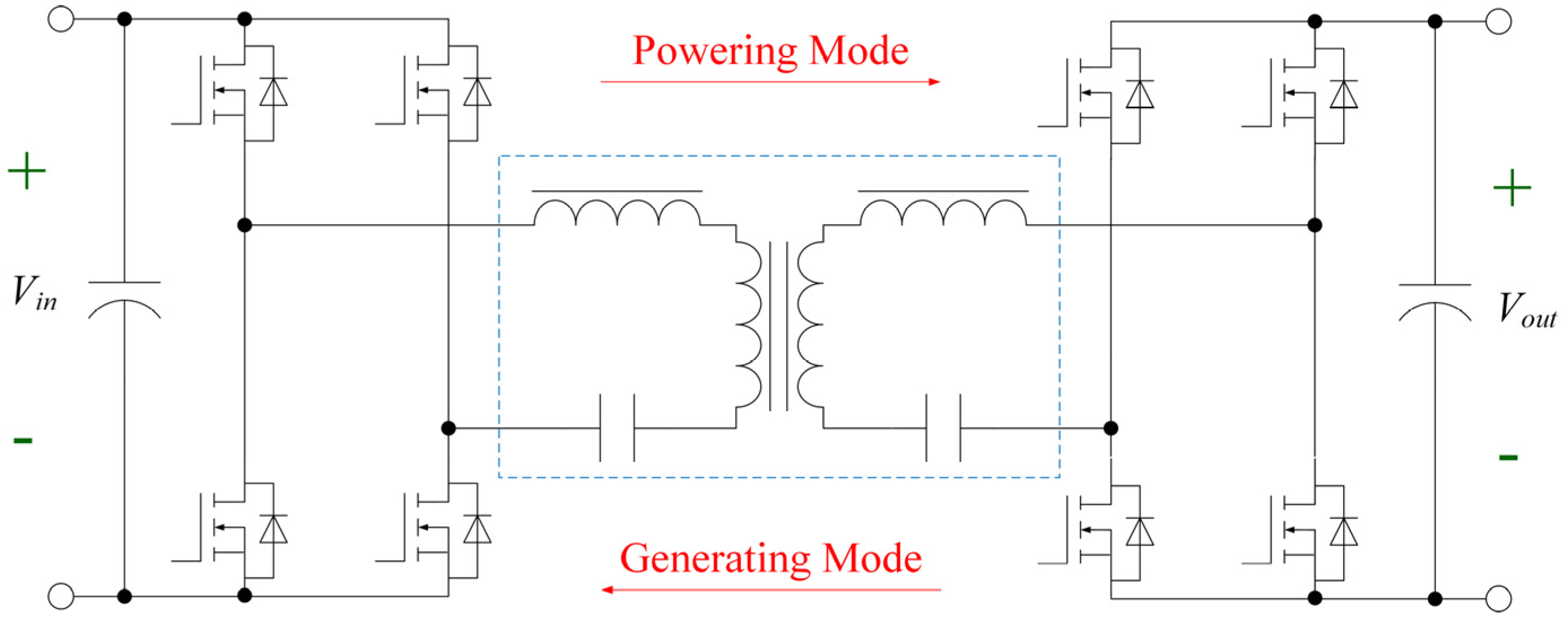
2. Coupling Mode Selection

Figure 5 shows the two different coupling patterns of the coupled inductor, and also their equivalent decoupling models [30]. As shown in Figure 5a, the direct coupling inductor with initial inductance L1, L2 can be modeled as one positive mutual inductance M at the common node, and two separate leakage inductors with inductance L1M and L2M, where M = kL. Correspondingly, the inverse coupling counterpart can be modeled as one negative mutual inductance -M at the common node, and two separate leakage inductors with inductance L1+M and L2+M as shown in Figure 5b. The voltages vL1, vL2 across L1, L2 now equal the summation of the voltage across mutual inductance and the leakage inductance.
Figure 5. Two different coupling patterns (a) Direct coupling; (b) Inverse coupling.
Energies 08 06399 g005
In order to investigate how the CIs influence the channel inductor ripple and the dynamic processing, typical operation waveforms of two-phase interleaved continuous current mode (CCM) Boost (TPICB) are shown in Figure 6.
Figure 6. Current curves when duty cycle is larger than 0.5 (a) Inverse coupling, (b) Direct coupling.
Energies 08 06399 g006
Figure 6a displays the current waveforms in inverse coupling mode, the dotted line represents the current waveforms of iL1, iL2 without coupling. Compared with the uncoupled counterpart, the current rising slope of iL2 in phase b-c is slower, due to the effect of the CI. At interval T1 and T3, the rising slope of the coupled inductors is greater. However, in TPICB circuits, the overlap time that the corresponding switches both on is short, so the total effect of the CI is to reduce the inductor current ripple. Moreover, in transient response phase, when output power increases, the ON time of switches will be increased and T1, T3 last longer, which will lead to fast dynamic response. This is another advantage by choosing the inverse coupling mode. Correspondingly, the current waveforms with direct coupling condition are shown in Figure 6b. The channel inductor ripple will be enlarged. Although above conclusions are obtained when D > 0.5, the same conclusion can be obtained when D < 0.5:
{ v L 1 = v L 1 M + v M v L 2 = v L 2 M + v M and { v L 1 = v L 1 + M + v M v L 2 = v L 2 + M + v M
For quantitative analysis, taking inverse coupling for example, some expressions will be given [30]. During phase T1, MOSFETs of channel 1 and 2 are turned on, voltages across L1, L2 are vL1 = vL2 = VL, therefore, the equivalent inductances for channel 1 and channel 2 are obtained:
{ V L = ( L 1 + M ) d i L 1 / d t M d ( i L 1 + i L 2 ) / d t V L = ( L 2 + M ) d i L 2 / d t M d ( i L 1 + i L 2 ) / d t
L T E Q 1 A = L M
L T E Q 2 A = L M
During T2 period, MOSFET of channel 1 is turned off, and MOSFET of channel 2 is turned on. Voltages across L1, L2 are vL1 = VLVH, vL2 = VL. Therefore, the equivalent inductance for channel 1 and channel 2 are calculated as:
L T E Q 1 B = L 2 M 2 L 1 D D M
L T E Q 2 B = L 2 M 2 L D 1 D M
During T3 period, MOSFETs of channel 1 and 2 are turned on. It’s the same as in time interval T1.
During T4 period, MOSFET of channel 1 is turned on, and MOSFET of channel 2 is turned off. It’s symmetry of the situation during T2:
L T E Q 1 D = L 2 M 2 L D 1 D M
L T E Q 2 D = L 2 M 2 L 1 D D M
Based on above analyses, to decrease the current ripple of low voltage input side, accelerate the auto current sharing process of switch capacitors, inverse coupling mode is selected in this paper.

3. Proposed Topologies and Operation Principles

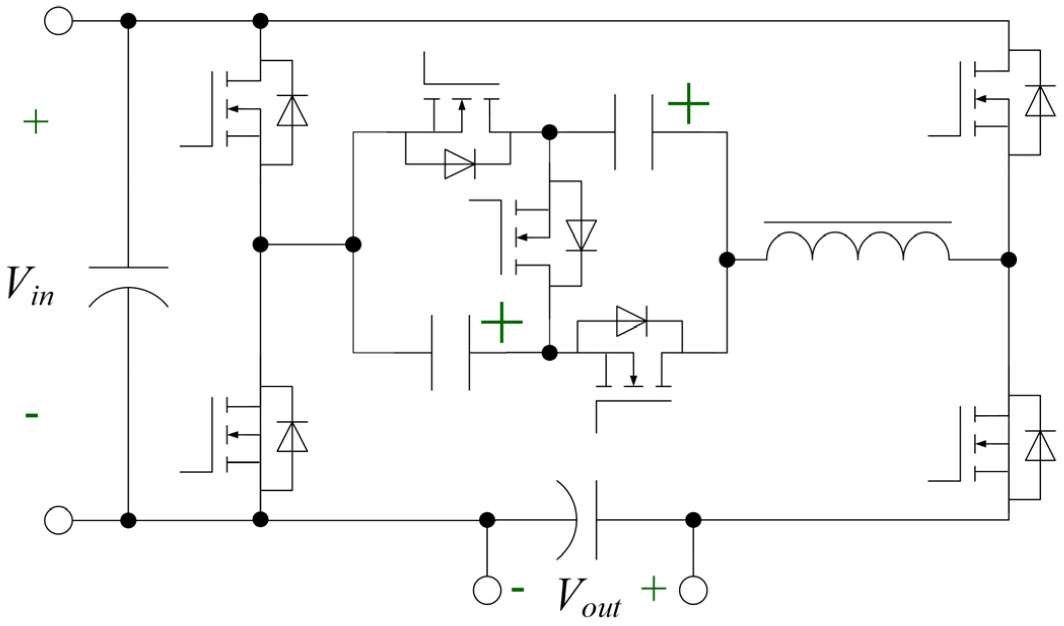
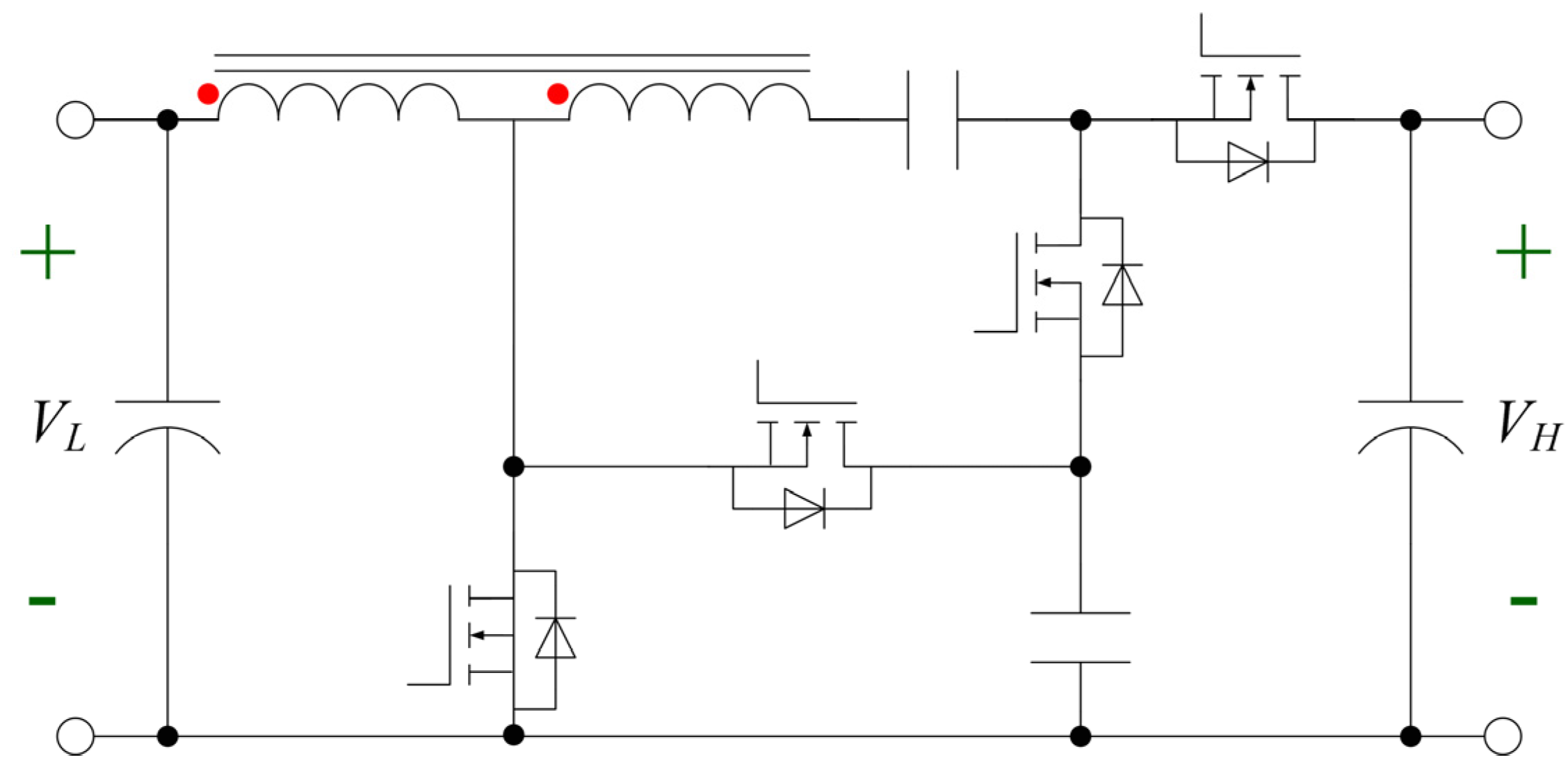
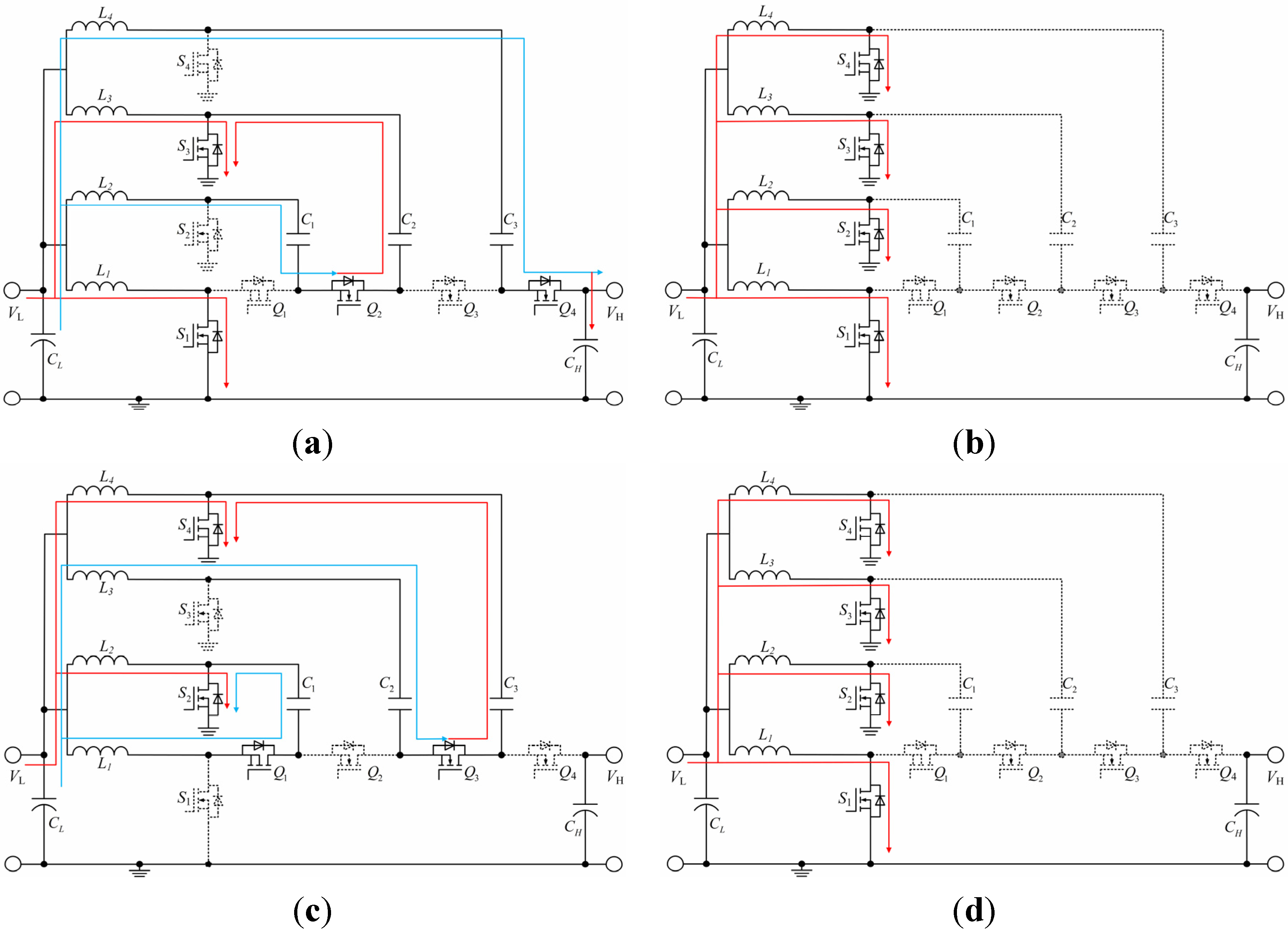
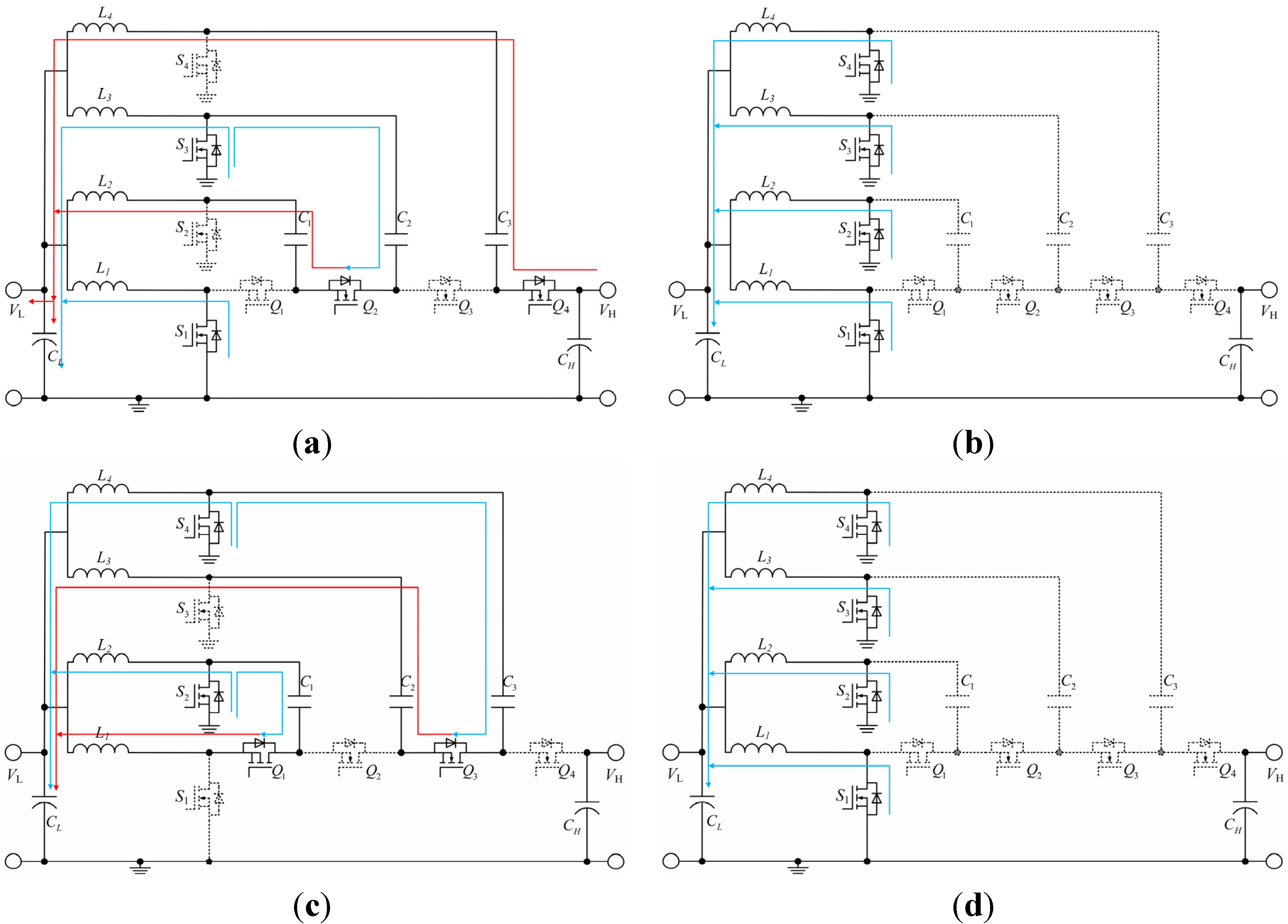
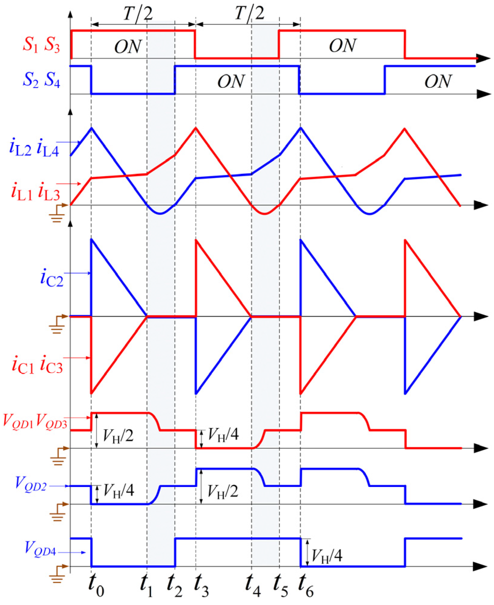
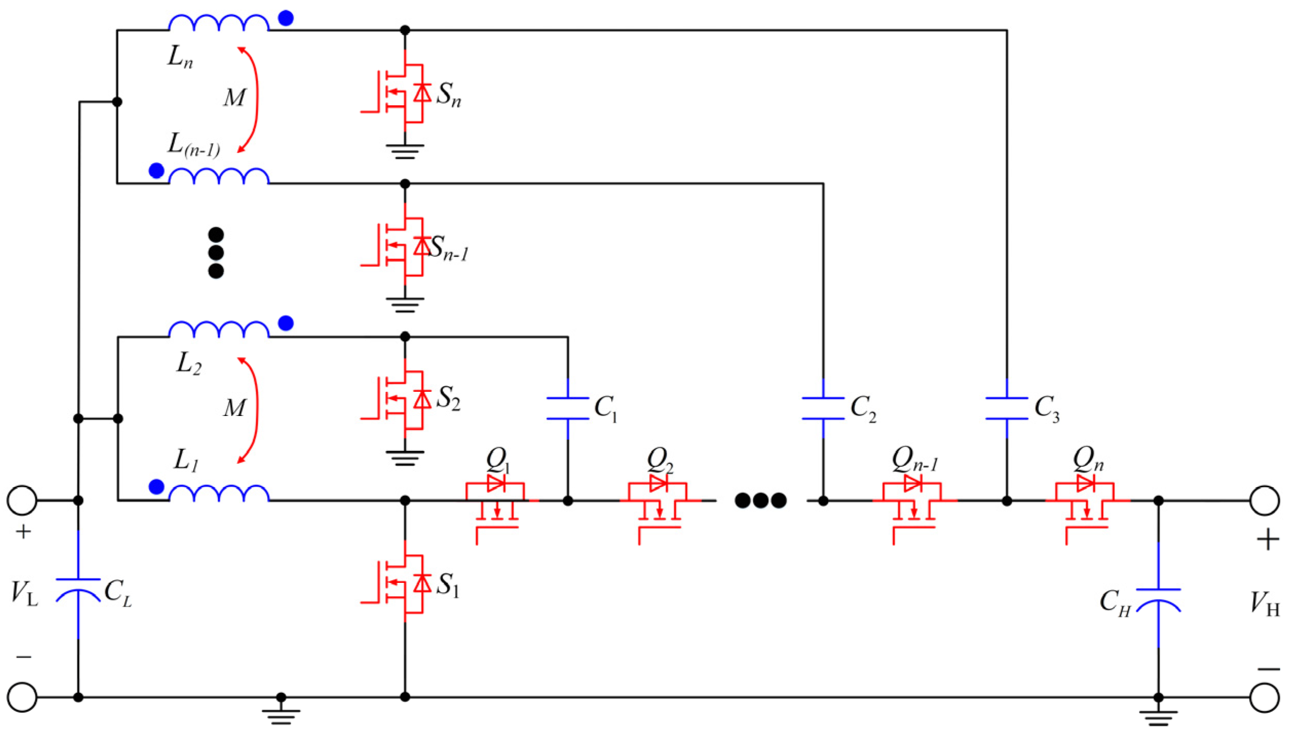
3.1. Proposed Topologies

Figure 7 shows the proposed HVCR BDC circuit after inductor decoupling. There are four parallel inductors at VL side, to reduce inductance and mitigate channel ripple current effectively, phases 1 and 2, as well as phases 3 and 4, share an inverse coupled inductor with a turn ratio of Np:Ns = 1:1. The coupling coefficient is denoted by k (0 < k < 1). In addition, there are three SCs connected in series in the circuit, SCs named C1, C2 and C3 are used in the circuit to realize HVCR, furthermore, with attendance of the SCs, the channel inductors can achieve auto current sharing (ACS) feature.
The PWM drive signal of the proposed circuit is very simple. Phases 1 and 3, as well as phases 2 and 4, share the same gate PWM signal. When the circuit works in Boost stage, energy flows from VL to VH; the duty cycle Dup of gate drive signals for S1, S2, S3 and S4 should be larger than 0.5 in order to eliminate circulating current during the turn-off of all ground-connected MOSFETs; and Q1, Q2, Q3 and Q4 are working in synchronous rectification (SR) mode during this time. Correspondingly, when the circuit works in Buck stage, energy flows from VH to VL; the duty cycle Ddown of PWM for Q1, Q2, Q3 and Q4 should be less than 0.5; and S1, S2, S3 and S4 are working in SR mode during this period.
Figure 7. Schematic of the proposed four-phase HVCR BDC.
Energies 08 06399 g007
During the following theoretical analyses and calculation process, the component parameters are regarded as identical, and the following three conditions are assumed:
(1)
All switches are treated as ideal.
(2)
L1 = L2 = L3 = L4 = L and C1 = C2 = C3 = C.
(3)
Capacitors C1, C2 and C3 are large enough that VC1, VC2 and VC3 are considered to be constant in a switching period.
(4)
The coupling coefficient k and the mutual inductance M of the CIs are equal, k = M/L, and the turn ratio of the CIs is equal to 1.

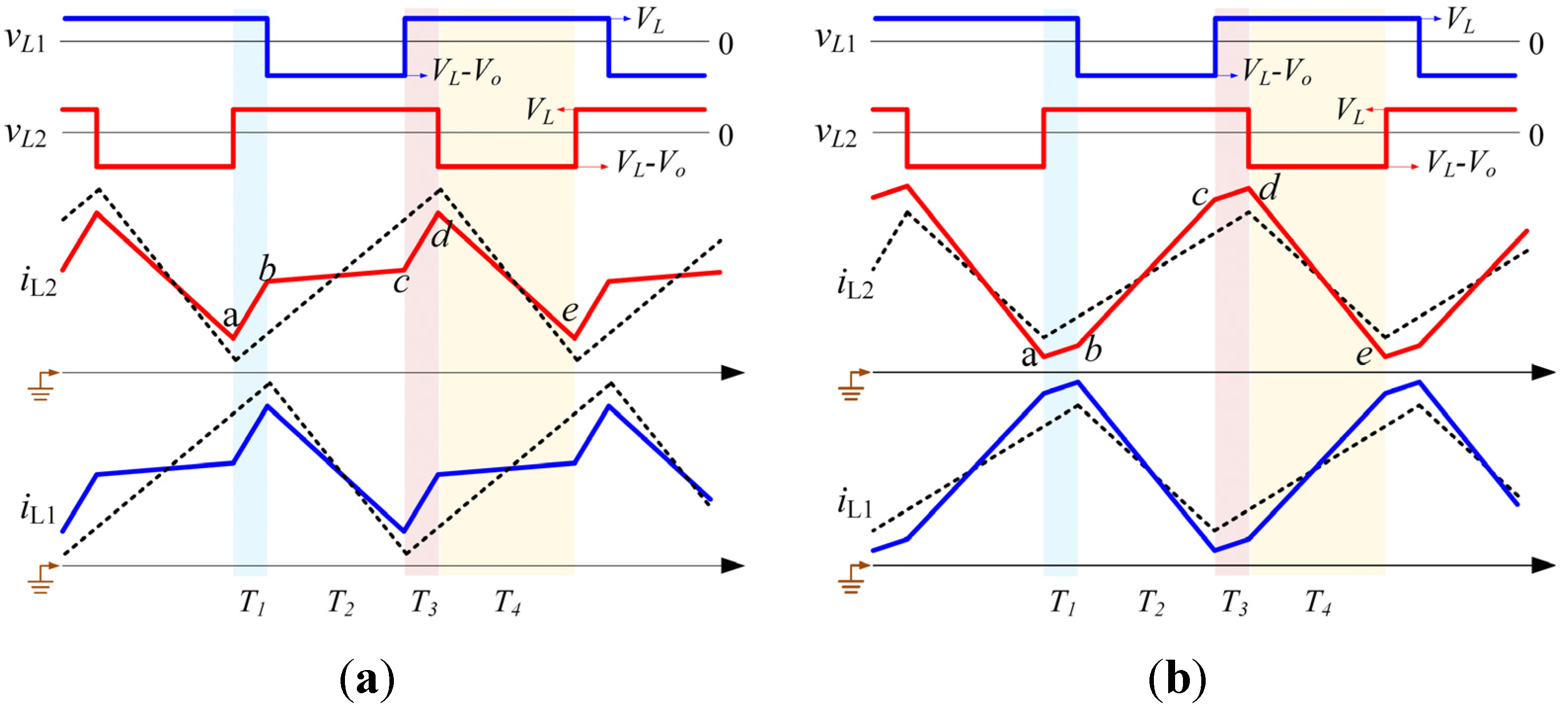
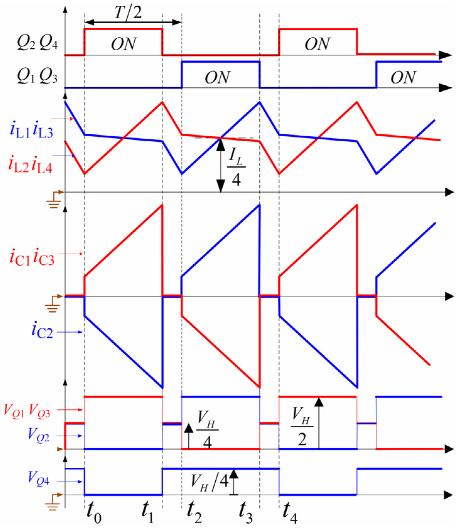
3.2. CCM Boost Stage

Figure 8 shows the major operating waveforms of the proposed HVCR BDC in CCM Boost stage. Figure 9 shows the equivalent circuits. In this mode, LVS energy flows from VL to VH. Switches S1, S2, S3 and S4 are operating in active switching with duty cycles of Dup and switches Q1, Q2, Q3 and Q4 are operated in SR mode, as shown in Figure 8. The operation of the CCM Boost stage can be divided into four intervals.
Figure 8. Operating waveforms for the CCM Boost stage.
Energies 08 06399 g008
Figure 9. Equivalent circuits in CCM Boost stage (a) interval 1; (b) interval 2; (c) interval 3; (d) interval 4.
Energies 08 06399 g009
Interval 1 [t0 ~ t1]: Power switches S1, S3 are on, and S2, S4 turn off. Inductor L1 are charged by VL, and inductor current iL1 goes up linearly. Inductor L2 is series-connected with C1 to charge capacitor C2, with inductor current iL2 going down linearly. Inductor L3 is charged by VL, and inductor current iL3 goes up linearly. Inductors L4 and C3 are series-connected to charge capacitor CH and the load, and inductor current iL4 goes down linearly. The voltage equations across inductors are obtained:
{ V L = L 1 d i L 1 / d t M d i L 2 / d t V L + V C 1 V C 2 = L 2 d i L 2 / d t M d i L 1 / d t V L = L 3 d i L 3 / d t M d i L 4 / d t V L + V C 3 V H = L 4 d i L 4 / d t M d i L 3 / d t
{ d i L1 d t = L V L + M ( V L + V C1 V C2 ) L 2 M 2 d i L3 d t = L V L + M ( V L + V C3 V H ) L 2 M 2
Interval 2 [t1 ~ t2]: Power switches S1, S2, S3 and S4 are turned on, and the corresponding SR switches Q1, Q2, Q3 and Q4 are turned off. Inductors L1, L2, L3 and L4 are charged by VL. Inductor currents iL1, iL2, iL3 and iL4 go up linearly. The load absorbs energy from CH. The voltage relationship of each inductor can be written as follows:
{ V L = L 1 d i L 1 / d t M d i L 2 / d t V L = L 2 d i L 2 / d t M d i L 1 / d t V L = L 3 d i L 3 / d t M d i L 4 / d t V L = L 4 d i L 4 / d t M d i L 3 / d t
d i L 1 d t = d i L 3 d t = V L L M
Interval 3 [t2 ~ t3]: Switches S1, S3 and Q2, Q4 are turned off, switches S2, S4 and Q1, Q3 are turned on. Inductor L1 release energy to C1 through Q1, with inductor current iL1 going down linearly. Inductor L2 is charged through VL, S2 path, and inductor current iL2 goes up in a linear way. Similarly, series-connected L3, VL, and C2 charge energy to C3 through Q3. Current iL3 goes down in a linear way. Inductors L4 are linearly charged by VL. The load is charged by CH. The voltage equations across inductors L1, L2, L3 and L4 are listed as following:
{ V L V C 1 = L 1 ​d i L 1 / d t M d i L 2 / d t V L = L 2 d i L 2 / d t M d i L 1 / d t V L + V C 2 V C 3 = L 3 d i L 3 / d t M d i L 4 / d t V L = L 4 d i L 4 / d t M d i L 3 / d t
{ d i L1 d t = ( V L V C1 ) L + M V L L 2 M 2 d i L3 d t = ( V L + V C2 V C3 ) L + M V L L 2 M 2
Interval 4 [t3 ~ t4]: As the state of mode 2, S1, S2, S3 and S4 are all turned on, and Q1, Q2, Q3 and Q4 are switched off. Inductors L1, L2, L3 and L4 are all linearly charged by VL.

3.3. CCM Buck Stage

Figure 10 and Figure 11 show the key waveforms and equivalent circuits in the CCM Buck stage, respectively.
Figure 10. Operating waveforms for the CCM Buck stage.
Energies 08 06399 g010
Figure 11. Equivalent circuits in CCM Buck stage (a) interval 1; (b) interval 2; (c) interval 3; (d) interval 4.
Energies 08 06399 g011
In this mode, HVS energy flows from VH to VL. Switches Q1, Q2, Q3 and Q4 are operating in active switching with duty cycles of Ddown and switches S1, S2, S3 and S4 are conducting in SR mode, as shown in Figure 10. The operation of the CCM Buck stage can be divided into four intervals.
Interval 1 [t0 ~ t1]: The switches Q2, Q4 and S1, S3 are turned on, while switches Q1, Q3 and S2, S4 are turned off. The inductor L4 and capacitor C3 are linearly charged by VH through Q4, C3, L4 and VL. Inductor current iL4 goes up linearly. The series-connected L2 and C1 are charged by C2, with linearly increasing inductor current iL2. Inductors L3, L1 linearly discharge energy to VL through S3 and S1 respectively. The voltage equations across each inductor are written as follows:
{ V L = L 1 d i L1 / d t M d i L2 / d t V C2 V L V C1 = L 2 d i L2 / d t M d i L1 / d t V L = L 3 d i L3 / d t M d i L4 / d t V H V L V C3 = L 4 d i L4 / d t M d i L3 / d t
Interval 2 [t1 ~ t2]: The power switches Q1, Q2, Q3 and Q4 are turned off, and S1, S2, S3 and S4 are turned on to reduce conductive losses. In this time period, the inductors L1, L2, L3 and L4 release energy to VL through S1, S2, S3 and S4 respectively. The voltage of SCs stay the same, with no current flowing (iC1 = iC2 = iC3 = 0). Therefore, the following relationships are derived:
{ V L = L 1 d i L1 / d t M d i L2 / d t V L = L 2 d i L2 / d t M d i L1 / d t V L = L 3 d i L3 / d t M d i L4 / d t V L = L 4 d i L4 / d t M d i L3 / d t
Interval 3 [t2 ~ t3]: The power switches Q1, Q3 and S2, S4 are turned on, while Q2, Q4 and S1, S3 are turned off. Inductor L1 is linearly charged by C1 with linearly increasing current iL1. Inductor L2 releases energy to VL with linearly decreasing iL2. Similarly, inductor L3 and capacitor C2 are charged by C3 through Q3. Inductor current iL3 goes up linearly. At the same time, inductor L4 discharges energy to VL through switch S4. Inductor current iL3 goes up linearly. The VL is charged by the summation of inductor currents iL1, iL2, iL3, iL4. The voltage equations across each inductor are written as follows:
{ V C1 V L = L 1 d i L1 / d t M d i L2 / d t V L = L 2 d i L2 / d t M d i L1 / d t V C2 V L V C1 = L 3 d i L3 / d t M d i L4 / d t V L = L 4 d i L4 / d t M d i L3 / d t
Interval 4 [t3 ~ t4]: It’s the same as Interval 2. The power switches Q1, Q2, Q3 and Q4 are turned off, and S1, S2, S3 and S4 are turned on to reduce conductive losses. In this time period, the inductors all release energy to VL through the corresponding current paths as shown in Figure 11d. Meanwhile, the voltage of switched-capacitors remain unchanged, iC1 = iC2 = iC3 = 0.

3.4. Discontinuous Current Mode (DCM) Boost Stage

Figure 12 shows the major operating waveforms of the proposed HVCR BDC in DCM Boost stage. In this mode, relative faint energy flows from VL to VH. Switches S1, S2, S3 and S4 are conducting in active switching with duty cycles of Dup and switches Q1, Q2, Q3 and Q4 are operating in SR mode, as shown in Figure 12. The operation of the DCM Boost stage can be divided into six intervals.
Figure 12. Operating waveforms for the DCM Boost stage.
Energies 08 06399 g012
Interval 1 [t0 ~ t1]: The same as interval 1 in CCM Boost mode: S1, S3 are on, and S2, S4 turn off. Inductor L1 is charged by VL, and inductor current iL1 goes up linearly. Inductor L2 is series-connected with C1 to charge capacitor C2, and inductor current iL2 goes down linearly. Inductor L3 is charged by VL, and inductor current iL3 goes up linearly. Inductor L4 and C3 are series-connected to charge capacitor CH and the load, and inductor current iL4 goes down linearly.
Interval 2 [t1 ~ t2]: The state of S1 and S3 are unchanged, but Q2 and Q4 are turned off. L1, L3 are charged by VL, with iL1, iL3 increasing linearly. Unlike interval 1, the current of C2 is zero, the output parasitic capacitors of S2 and S4 are resonant with channel inductors respectively. iL2, iL4 will increase firstly and then decrease positively, and their peak values are related with the value of output parasitic capacitances. When iL2 and iL4 reach zero, ZVS turn-on of S2 and S4 can be achieved at this time, and if S2 and S4 still not be turned on, iL2 and iL4 will begin the oscillation of positive phase.
Interval 3 [t2 ~ t3]: The same as interval 2 in CCM Boost mode, power switches S1, S2, S3 and S4 are turned on, and Q1, Q2, Q3 and Q4 are turned off. Inductors L1, L2, L3 and L4 are charged by VL. Inductor currents iL1, iL2, iL3 and iL4 go up linearly. The load absorbs energy from CH.
Interval 4 [t3 ~ t4]: The same as interval 3 in CCM Boost mode, switches S1, S3 and Q2, Q4 are turned off, while switches S2, S4 and Q1, Q3 are turned on. Inductor L1 releases energy to C1 through Q1, and inductor current iL1 goes down linearly. Inductor L2 is charged through VL, S2 path, and inductor current iL2 goes up in a linear way. Similarly, series-connected L3, VL and C2 charge energy to C3 through Q3. Current iL3 goes down in a linear way. Inductor L4 is linearly charged by VL. The load is charged by CH.
Interval 5 [t4 ~ t5]: This interval is the continuation of interval 4. Switches S1, S3 and Q2, Q4 are turned off, switches S2, S4 are turned on when iL2 and iL4 decrease to zero. During this interval, iL2, iL4 increase linearly. Similar to interval 2, the current of C1 and C3 is zero, and the output parasitic capacitors of S1 and S3 are resonant with channel inductors respectively. iL1, iL3 will increase firstly and then decrease positively, and their peak values are related to the value of output parasitic capacitances of selected MOSFETs. When iL1 and iL3 reach zero, ZVS turn-on of S1 and S3 can be achieved at this time, and if S1 and S3 still not be turned on, iL1 and iL3 will begin the oscillation of positive phase.
Interval 6 [t5 ~ t6]: As the state of interval 3, S1, S2, S3 and S4 are all turned on, and Q1, Q2, Q3 and Q4 are switched off. Inductors L1, L2, L3 and L4 are all linearly charged by VL.
Based on the above analyses, it can be seen that, channel inductor will resonant with the output parasitic capacitor of the corresponding MOSFET in DCM mode, which will lead to negative oscillation of the inductor current other than constant zero. Moreover, the negative oscillation peak is determined by the value of output parasitic capacitor for the selected MOSFET. In this paper, silicon carbide (SiC) MOSFETs are selected due to their very tiny output parasitic capacitor. Furthermore, ZVS turn-on of the relevant MOSFET can be achieved in turning on the switch during the negative oscillation of the inductor current, which will improve the circuit light-load efficiency further.

4. Feature Analysis and Design Considerations

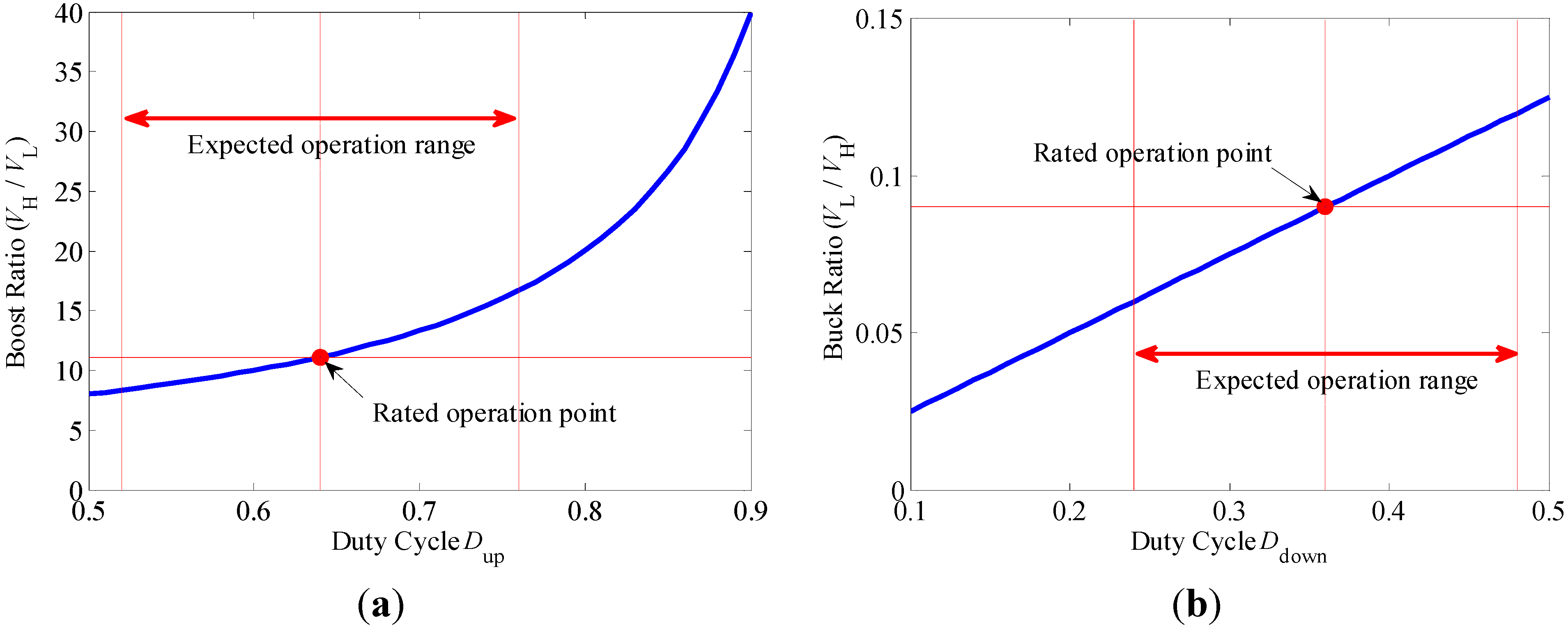
4.1. Voltage Gain and Duty Ratio

By adopting energy conservation method for L1, the following express can be obtained:
Δ E = L 1 i L1 2 ( t 4 ) / 2 L 1 i L1 2 ( t 0 ) / 2 = 0
This indicates the total inductor current increment is zero in a switching period, as in Equation (19), with the time periods of each mode listed in Equation (20):
{ MODE1 d i L1 + 2 MODE2 d i L1 + MODE3 d i L1 = 0 MODE1 d i L3 + 2 MODE2 d i L3 + MODE3 d i L3 = 0
{ T MODE1 = T MODE3 = ( 1 D u p ) T s T MODE2 = T MODE4 = ( D u p 1 / 2 ) T s
where tMODE1, tMODE2, tMODE3 and tMODE4 are the duration time of each corresponding mode.
Substitute Equations (10), (12) and (14) in (19), following equations are therefore deduced:
{ L [ V L ( 1 D u p ) V C1 ] + M [ V L + ( 1 D u p ) ( V C1 V C2 ) ] = 0 L [ V L + ( 1 D u p ) ( V C2 V C3 ) ] + M [ V L + ( 1 D u p ) ( V C3 V H ) ] = 0
Due to the effect of voltage doubling cells based on SCs, VH = 4VC3/3 = 4VC2/2 = 4VC1/1. Then solving Equation (21), we get:
{ V L ( 1 D u p ) V C1 = 0 V L + ( 1 D u p ) ( V C1 V C2 ) = 0 V L + ( 1 D u p ) ( V C2 V C3 ) = 0 V L + ( 1 D u p ) ( V C3 V H ) = 0
In consequence, voltage gain for the proposed 4-phase BDC topology in CCM Boost stage can be obtained:
M H = V H / V L = 4 / ( 1 D up )
Similarly, the voltage gain in CCM Buck stage is deduced as:
M L = V L / V H = D down / 4
The relationship between the voltage ratio and duty ratio of the proposed 4-phase BDC is sketched in Figure 13.
Figure 13. Duty cycles versus voltage gain (a) CCM Boost operation; (b) CCM Buck operation.
Energies 08 06399 g013
(1)
The voltage ratio of the proposed BDC is extended significantly, with duty cycle D varies from 0.5 to 0.9 (Dup) or 0.1 to 0.5 (Ddown), the voltage ratio can achieve 8 - 40 in CCM Boost operation, and 0.025 - 0.125 in CCM Buck operation.
(2)
Within the whole working scope, the voltage gain varies evenly when the duty cycle is changing, which is conductive to the design of the closed-loop digital controller.

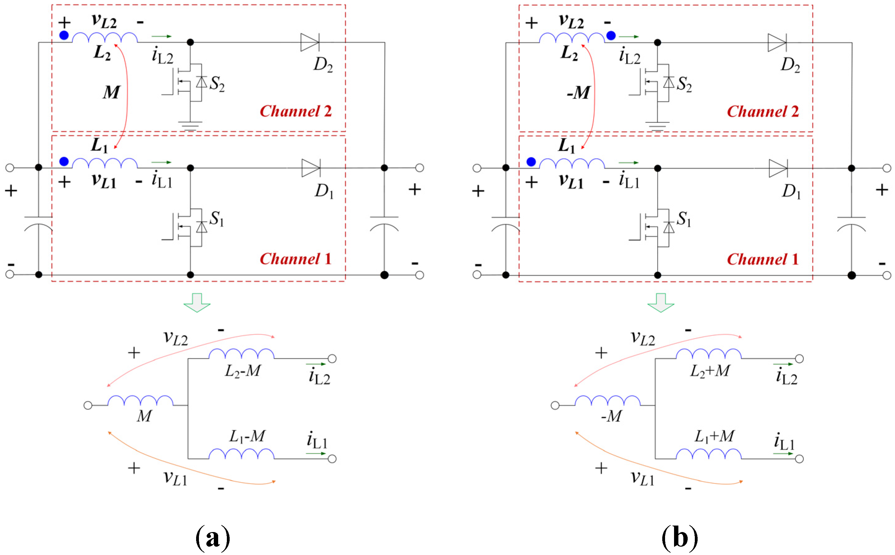
4.2. Auto Current Sharing

As mentioned above, due to the effects of the series SCs between the four channels, the ACS mechanism of the proposed BDCs is different from traditional parallel circuits. In theory, for static current sharing, even with different inductor values, the proposed BDCs can achieve ACS, if the same duty cycle of each channel MOSFET is fulfilled. Based on Figure 8 and above analysis, a case study of CCM Boost stage will be given. The current expressions for SCs can be obtained as:
{ i C1 = ( 1 S 1 S 3 ) i L1 ( 1 S 2 S 4 ) i L2 i C2 = ( 1 S 2 S 4 ) i L2 ( 1 S 1 S 3 ) i L3 i C3 = ( 1 S 1 S 3 ) i L3 ( 1 S 2 S 4 ) i L4
where S1, S2, S3 and S4 = “0” or “1” are the switching state of the corresponding power switches. The Ampere-second balance equation can be expressed as follows:
{ I L2 ( t 1 t 0 ) + I L1 ( t 3 t 2 ) = 0 I L2 ( t 1 t 0 ) I L3 ( t 3 t 2 ) = 0 I L4 ( t 1 t 0 ) + I L3 ( t 3 t 2 ) = 0
where IL1, IL2, IL3 and IL4 represent the mean value of corresponding inductor current during time interval [t2, t3] or [t0, t1]. The time-period of t3t2 equals to t1t0 when S1, S2, S3 and S4 with the same duty cycle Dup, and therefore IL2 = IL1 is obtained. In the same way, IL2 = IL3, IL3 = IL4 are derived. Based on above analysis, ACS among each inductor can be achieved if the switches S1, S2, S3 and S4 share the same turn-on duty cycle.
Capability of ACS is a significant advantage for the proposed 4-phase BDC, which can simplify the design of CIs and the digital controller. Unfortunately, the regulation process of ACS leads to current pulsation, and even instability of the whole system. To solve this negative effect, a sufficiently small inductance value and a relatively large SC value should be selected based on the above optimization methods. A small inductance is used to shorten the ACS process, and a large SC is used to minimize the voltage fluctuation between SC and input/output capacitors. Besides, a carful designed digital control loop is used to guarantee the stability of the proposed BDC, as shown in Figure 14. With the control loop compensation, low-frequency gain is enlarged, several resonant peaks caused by SCs are weakened, and the cut off frequency of the current loop is decreased to 35.8 kHz and the system is stable with good phase margin (PM) and gain margin (GM).
Figure 14. Bode diagram with and without the loop compensation.
Energies 08 06399 g014

4.3. Design Considerations

4.3.1. Optimal Design of the CIs

In this section, the following analyses are mainly aim to optimize the coupling coefficient of the CIs to minimize inductor current ripple on the premise that the inductance and inductor volume are small enough. Under uncoupled mode, assumes that the inductor ripple current of the design target is less than 1 A, and its value can be calculated by the following expressions in Boost mode:
L = D u p V L Δ i L f s
where ΔiL = 1 A is the expected inductor current ripple, and VC3 is the average voltage of C3. And finally the minimum inductance under uncoupled mode Lmin = 125 µH is calculated.
As mentioned above, small inductance can accelerate the ACS process, increase system stability. What’s more, smaller inductance can reduce the volume of coupled-inductors as well as increase power density. Thus, without considering the inductor current ripple, winding losses and phase cross-over frequency, smaller inductance should be adopted. However, considering smaller inductors will lead to larger ripple current and inductor losses, CIs are used to reduce the current ripple further, on the premise that with the same initial inductance Lmin. Take CCM Boost stage for example, Figure 8 shows that the inductor ripple current equals to the current decrement of L1 during time interval [t2t3], which is proportional to the equivalent inductance LEQ1 within the same period:
d i L1 d t = L ( V L V C1 ) + M V L L 2 M 2
where Vc1 = 4VL/(1 − Dup), and M = kL. Then:
d i L1 d t = V L ( 1 1 1 D up + k ) ( 1 k 2 ) L
{ D ( d i L1 d t ) = D up 1 V L ( 1 D up ) 2 ( 1 k 2 ) L k ( d i L1 d t ) = V L ( 1 k 2 ) L + 2 V L ( 1 1 1 D up + k ) k L ( 1 k 2 ) 2 L 2 L ( d i L1 d t ) = ( 1 k 2 ) L V L ( 1 1 1 D up + k ) ( 1 k 2 ) ( 1 k 2 ) 2 L 2
Equation (30) describes the relationship between LEQ1, Dup, k and L1. When Equation (30) equals to zero, the relevant maximum equivalent inductance will be obtained. Thus, with the same inductance and different coupling coefficients, the ripple current can be minimized if the equivalent inductance LEQ1 reaches a maximum:
k = ( D u p 2 D u p 1 ) / ( 1 D u p )
In the same way, the optimal k value corresponding to the global maximum LEQ2 in CCM Buck stage can be obtained:
k = ( 1 D d o w n 1 2 D d o w n ) / ( D d o w n )
Based on the expression Equations (30)–(32), Figure 15 can be obtained, and we can see that:
(1)
With a smaller initial channel inductance, a more tiny variation of the equivalent inductance with changing Dup/Ddown will be obtained, which indicates a smaller input ripple current in the range of any load condition;
(2)
The maximum equivalent inductance is related to duty cycle Dup or Ddown, for example, if rated Dup equals to 0.64 or Ddown equals to 0.36, then the optimized coupling coefficient is k = 0.3. It is obviously that the optimized k value in CCM Boost operation and CCM Buck operation is equal, when rated VL and VH are given.
Figure 15. Equivalent inductance curves versus k and D (a) CCM Boost; (b) CCM Buck.
Energies 08 06399 g015
According to the above two conclusions and the Lmin under uncoupled mode, finally, L = 120 µH and k = 0.3 can be selected, where k = 0.3 is the optimum solution of the coupling coefficient under rated load condition.

4.3.2. Optimal Design of SCs

According to the assumed conditions in Section 3.1, to facilitate the circuit analyses and calculations, voltage ripple across SCs has been ignored. However quantitative analysis of the ripple voltage across SCs is necessary to guarantee the feasibility of the assumed conditions. It is generally known that the voltage ripple across switched-capacitors C1, C2 and C3 can be expressed as:
Δ U C = I C ( 1 D up ) f S C
where IC is the mean value of the SCs current iC during a switching period Ts:
I C = P o V H ( 1 D up )
Assume that the voltage ripple of each SC is lower than 0.5 V, according to above expression, Cmin = 21 µF can be calculated. Considering the ripple voltage caused by ESR, parasitic inductance and thermal effect of capacitors in applications, 40 µF/500 V metalized-polyester film capacitors are selected. Because of its excellent characteristics like the high frequency performance, low ESR, low dielectric dissipation factor and high di/dt or du/dt capabilities. Its ESR is only about 5 m Ohm, and RMS current is about 19 A at 10 kHz, which is exactly suitable for the proposed high-frequency and large-current switching capacitor application.

4.3.3. Selection of Power MOSFETs

According to operation analysis in Section 3.2 and Section 3.3, the voltage stress of the power switches S1 - S4 and Q4 is VH/4, while for Q1, Q2 and Q3, the voltage stress is VH/2 in either CCM Boost or CCM Buck stage. Furthermore, when the circuit works in discontinuous current mode (DCM), all switches S1 - S4 and Q1 - Q4 will suffer VH/2 voltage stress. In all of the normal states, the voltage stress of power switches only relate to the value of VH, no matter with duty cycle, value of VL or load variations. From Figure 8 we can see that the voltage gain in Boost/Buck stage is 4 times of the conventional Boost/Buck converter, while the voltage stress is only one half.
The maximum current through S2, S3 and S4 occurs at their turn off instant, superimposed by two inductor currents, which is calculated as:
i S = 2 P o V H ( 1 D up ) + V L ( D up 0.5 ) L EQ2D f S
where LEQ2D represents the equivalent inductance of channel 2 in Mode 4, which can be easily obtained with the method given in Section 2. Similarly, the maximum currents through Q1, Q2, Q3 and Q4 occur at their turn on instant, given as:
i Q = P o V H ( 1 D up ) + ( V H / 4 V L ) ( 1 D up ) 2 L EQ2A f S
where LEQ2A represents the equivalent inductance of channel 2 in Mode 1. In addition, the above expression is also suitable for switch S1, because when S1 turns off, the current iL1 all transfer from S1 to Q1. It indicates the current stress for S1 is smaller compared to S2, S3 and S4, owing to only one inductor current iL1 flowing through.
According to Equations (35), (36) and the analysis above, the maximum current through S1 - S4 and Q1 - Q4 and the maximum voltage stress can be obtained easily. Moreover, in order to minimize the parasitic output capacitance and decrease the negative resonant current peak in DCM mode, increase the operating frequency as well as the power density and guarantee the conversion efficiency, SiC Power MOSFETs have been selected.

4.4. Losses Distribution

4.4.1. Conduction Losses on MOSFETs

For MOSFET S1, the average current during its ON state is mean inductor current IL1, so the conduction losses of S1 can be calculated based on the Joule principle as follows:
P C M S 1 = I L1 2 R ds-on D u p
where Rds-on is the MOSFET conduction resister, and Dup is the conduction time of S1 in one switching period. In a similar way, the heat losses of Q1 is obtained as:
P C M Q 1 = I L1 2 R ds-on ( 1 D u p )
where (1 − Dup) is the conduction time of Q1 in one switching period. Furthermore, it can obtained that: IL1 = IL2 = IL3 = IL4 = IL/4, with precondition: D1 = D2 = D3 = D4 = Dup. Thus the above expression is also suitable for Q2, Q3 and Q4.
In reference to switches S2, S3 and S4, the current flowing through is larger than S1 due to two inductor currents superimposed. For switch S2, the heat losses result from average inductor current IL1 and IL2 according to analyses in Section 3.2. In Mode 2, S2 and S1 are ON (duration of time: (Dup − 0.5)·Ts), the current through S2 is just iL2 according to steady state waveforms shown in Figure 8, thus the average current in Mode 2 is calculated as:
I S2-M2 = I L2 + V L V C 1 2 L E Q 2 A ( 1 D u p ) T s + V L ( D u p 0.5 ) T s 2 L E Q 2 B
where LEQ2A and LEQ2B are the equivalent inductance for channel 2 in Mode 2 and Mode 4 respectively. In Mode 3, S2 ON and S1 OFF (Duration of time: (1 − DupTs), the current through S2 is the sum of iL1 and iL2. That is:
I S2-M3 = I L1 + I L2 = I L 2
In Mode 4, S2 ON, S1 OFF (Duration of time: (Dup − 0.5Ts), the current iL1 is removed from S2. Therefore, the average current through S2 in Mode 4 is calculated based on waveforms in Figure 8:
I S2-M4 = I L2 V L V C 1 2 L E Q 2 A ( 1 D u p ) T s V L ( D u p 0.5 ) T s 2 L E Q 2 B
Combine Equations (40)–(42), and the total conduction losses of S2 is expressed as:
P C M S 2 = I S2-M2 2 R ds-on ( D u p 0.5 ) + I S2-M3 2 R ds-on ( 1 D u p ) + I S2-M4 2 R ds-on ( D u p 0.5 )
Due to the circuit symmetry, the conduction losses of S3, S4 are equal to Equation (42).

4.4.2. Switching Losses of MOSFETs

The switching losses are composed of turn-on, turn-off losses and the free-wheel diode (FWD) losses. PWD losses is ignored considering that the mechanism of SR mode. According to reference [31,32,33], the calculation expression of turn-on and turn-off losses are obtained as:
{ P SW-ON = 1 2 Δ U o n i o n T s w o n f s P SW-OFF = 1 2 Δ U o f f i o f f T s w o f f f s
where ΔUoff represents the voltage level altering value before/after turn-off transient, and for each MOSFET, ΔUoff = 100 V is always right. Tsw-off is the turn-off crossing time. ΔUon is also about 100 V for each switch, which is obtained from Figure 8. And Tsw-on is the turn-on overlap time.
In a same switching point, the instantaneous current value of S1, S2, S3 and S4 at turn-off moment ioff-S is equal to the instantaneous current value of Q1, Q2, Q3 and Q4 at turn-on moment ion-Q, and then:
i o f f S = i o n Q = I L 1 + ( V C 1 V L ) ( 1 D u p ) 2 L E Q 1 C f s
In a similar way:
i o n S = i o f f Q = I L 1 ( V C 1 V L ) ( 1 D u p ) 2 L E Q 1 C f s
Based on Equations (43)–(45), the switching losses of all MOSFETs can be obtained.

4.4.3. Capacitor ESR Losses

The power losses on capacitors is proportional to ripple current and total dissipation resistor ESR. And the equation for switching capacitor C1 is given as:
P S C 1 = Δ i L1 2 R C E S R ( 1 D u p )
In reference to SCs C1, C2, C3, the ripple current is just the inductor current ripple ΔiL. While for filter capacitors, the ripple current refer to input/output current ripple.

4.4.4. ESR Losses of CIs

The heat consumption on each inductor is proportional to its average current and the parasitic resistor. That is:
P L E S R = I L 2 R L E S R

4.4.5. Magnetic Losses of CIs

The magnetic losses of coupled inductors can be calculated as [34]:
P L C O R E = p w W t F e
where WtFe is the total weight of the selected core, and pw is the losses on unit weight, the unit is: mW/g, and the pw can be found out from datasheet.

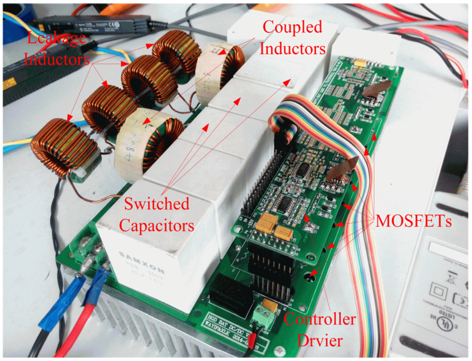
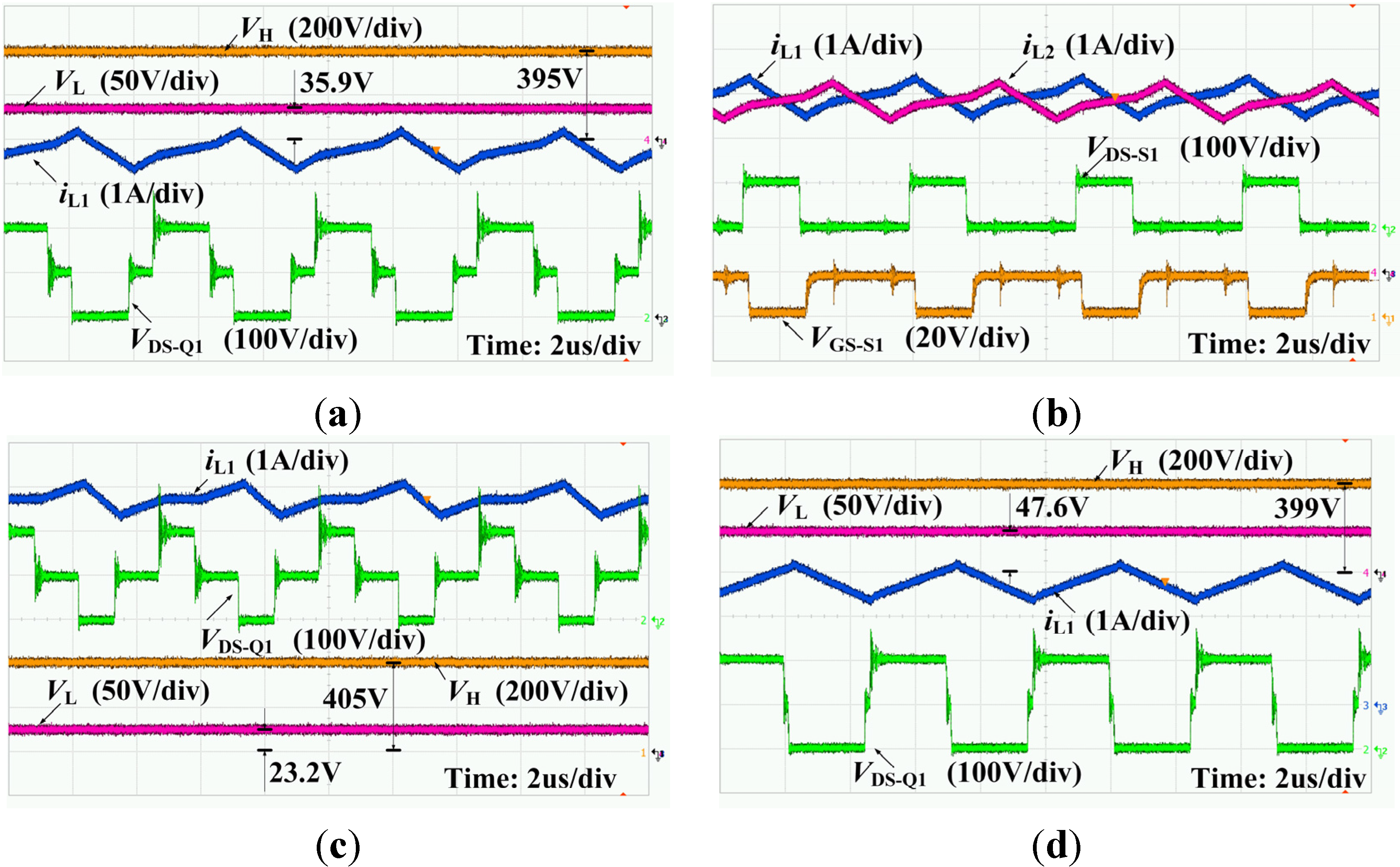
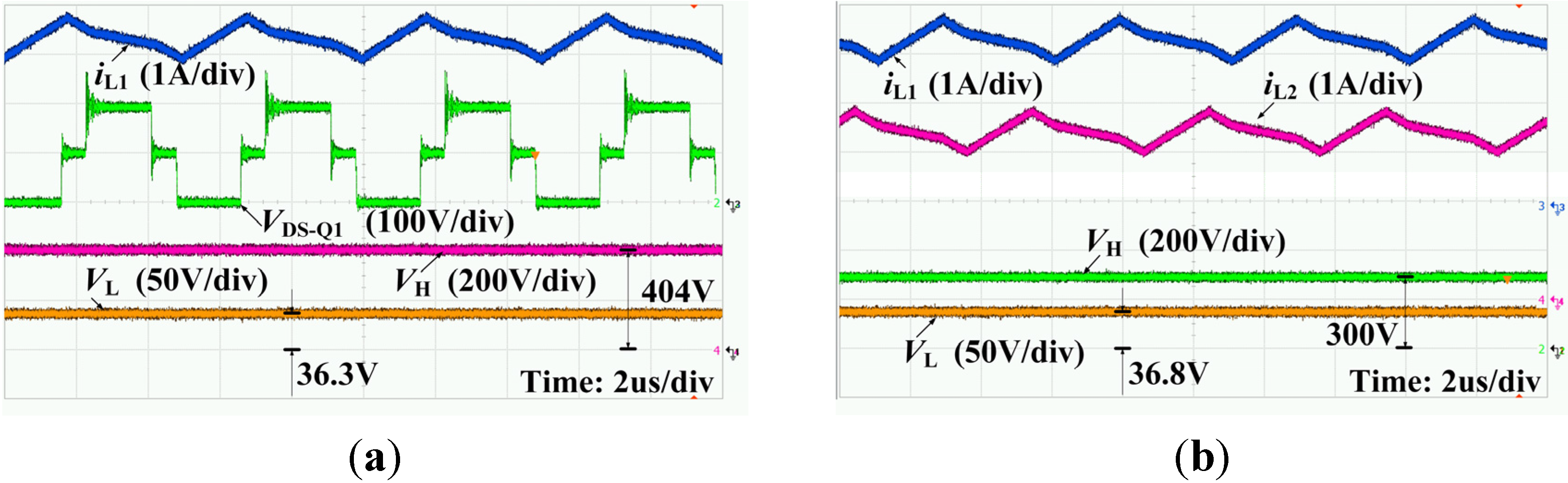
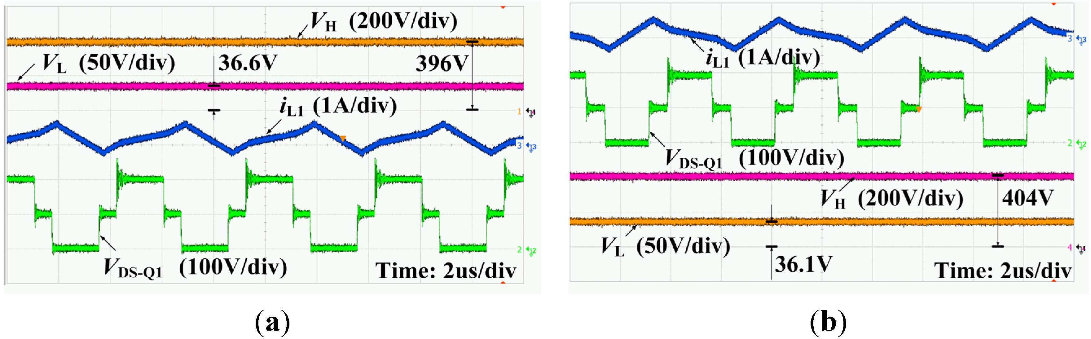
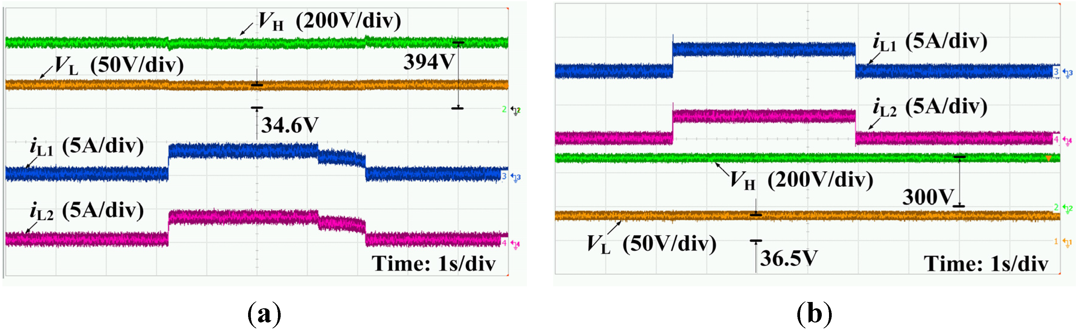
5. Experimental Results

The experiments are performed under voltage and current closed-loop conditions. The output/input voltage acquisition is simply achieved by voltage-splitter resistances, and the inductor current acquisition utilizes a LAH 25-NP current transducer. According to the analysis in Section 4.2, the average inductor currents are identical to each other i.e., IL1 = IL2 = IL3 = IL4, assuming that D1 = D2 = D3 = D4 = Dup. Based on this fact, channel current transducers can be reduced to just one. The experimental results of channel current comparison shown in the following figures are just the results with the effect of ACS fulfilled by SCs, there is no other additional current-sharing controller. This would dramatically reduce circuit complexity, cost and controller design.
As illustrated in Figure 16, a 500 W prototype converter is built in the laboratory. It can be seen that each of the CIs is constituted with two separated leakage inductors and a strong coupling (k = 0.95) transformer, which is used to reduce the difficulty of CIs construction (k = 0.3). Moreover, with limited selectable types, S1 to S4 as well as Q1 to Q4 are the same type of SiC MOSFET: C2M0080120D. In addition, isolated driver circuit based on pulse transformer is used as the driver circuit of those MOSFETs. S1 and Q1 (the same as S2 and Q2, or S3 and Q3, or S4 and Q4) share a drive circuit, and complementary symmetrical PWM driving signals will be supplied to S1 and Q1 (the same as S2 and Q2, or S3 and Q3, or S4 and Q4) respectively. In this way only four identical drive circuits are needed, which can effectively reduce the complexity of the driving circuits.
Figure 16. Picture of the laboratory setup.
Energies 08 06399 g016
Based on above analyses and optimization methods, the optimized parameters are shown in Table 1.
Table 1. Specifications of the prototype circuit.
Parameters and componentsValues (units)
Rated power Pn500 W
Low side input DC voltage VL24–48 V
High side input DC voltage VH400 V
Operating frequency (fS)200 kHz
Power MOSFETsC2M0080120D
Switched capacitors (C1, C2, C3)40 μF
Input/Output Capacitors (CL, CH)80 μF
ESR (C1, C2, C3, CL, CH)5 m Ohm
Inductance of channel 1 (L1)122 μH
Inductance of channel 2 (L2)128 μH
Inductance of channel 3 (L3)124 μH
Inductance of channel 4 (L4)126 μH
Coupling coefficient (k)0.3
Weight of magnetic core25.2 g
Core loss per unit weight20 mW/g
Length of magnetic path8.95 cm
Number of turns48
ESR (L1, L2, L3, L4)30 m Ohm
Figure 17a,c,d show the input and output voltages, channel 1 inductor current, and drain-source voltage of Q1 in CCM Boost mode under different input voltages (24 V to 48 V). It can be seen that inductor current ripples are less than 1 A in the entire input voltage range, and voltage stress across Q1 is about 200 V. When VL side voltage varies from 24 V to 48 V, output voltage VH fluctuates between 395 V and 405 V. As shown in Figure 17c, when VL = 23.2 V, each channel average inductor current is about 5.5 A, and peak value is about 6 A. Figure 17b shows channel 1 and channel 2 inductor current waveforms, drain-source and gate-source voltages of S1 in rated CCM Boost mode. Combine this figure with the inductances given in Table 1, it can be seen that when inductance deviation among L1, L2, L3 and L4 are less than ±5%, the coefficient of ACS executed by SCs will be greater than 0.95 (Just the effect of ACS fulfilled by SCs, without extra current-sharing control). Furthermore, voltage stress across S1 is about 100 V.
Figure 17. Experimental waveforms under CCM Boost mode (a) and (b) 36 V to 400 V; (c) 24 V to 400 V; (d) 48 V to 400 V.
Energies 08 06399 g017
Figure 18 displays the experimental results obtained in CCM Buck stage under 400 V (or 300 V) input and 36 V output. Figure 18a gives the input and output voltages, channel 1 inductor current, and drain-source voltage of Q1. It can be seen that inductor current ripples remain less than 1 A when the output voltage VL = 36 V. Voltage stress across Q1 is still approximately 200 V. Figure 18b shows the channel 1 and channel 2 inductor currents, input and output voltages, it can be seen that the coefficient of ACS is still larger than 0.95.
Figure 18. Experimental waveforms under CCM Buck stage (a) 400 V to 36 V (b) 300 V to 36 V.
Energies 08 06399 g018
Figure 19 shows the experimental waveforms of the input and output voltages, channel 1 inductor current, and drain-source voltage of Q1 under light-load conditions. Figure 19a is the waveforms of Boost mode with 15.7 W output power, and Figure 19b shows the waveforms of Buck mode with 13 W output power. Therefore, the proposed BDC can achieve quasi-critical inductor currents even under tiny load conditions. Moreover, as shown in Figure 19, ZVS turn-on for each switch is achieved under light-load conditions, which is beneficial to the light-load efficiency optimization.
Figure 19. Experimental results in light-load condition (a) 36 V input and 400 V/10 k Ohm output; (b) 400 V input and 36 V/100 Ohm output.
Energies 08 06399 g019
Figure 20 gives the dynamic response of the proposed BDC against load variation. Figure 20a shows the input and output voltages, channel 1 and channel 2 current waveforms with 34.6 V input and 394 V output. During this time period, load resistance is changed between 10 k Ohm and 320 Ohm. It can be seen that output voltage variation is less than 15 V. Figure 20b shows the input and output voltages, channel 1 and channel 2 current waveforms when input is 300 V and output 36.5 V. At this time, load resistance is changed between 100 Ohm and 2.5 Ohm. It can be seen that output voltage variation is less than 10 V. Therefore, fast and stabilized dynamic responses are achieved.
Figure 20. Dynamic response of the proposed BDC against load variation (a) load resistance variation between 10 k Ohm and 320 Ohm; (b) load resistance variation between 100 Ohm and 2.5 Ohm.
Energies 08 06399 g020
The measured efficiency of the proposed BDC is depicted in Figure 21a, and the test result is based on YOKOGAWA WT3000 data, with a basic power accuracy of ±0.02% of reading, DC and 0.1 Hz–1 MHz measurement bandwidths. When the output power is 500 W, the efficiency under CCM Boost stage and CCM Buck stage are about 96.1% and 94.8% respectively. Benefit from the margin of the selected devices and heat sink, during the experiment, the maximum output power of the proposed converter has been raised to 1 kW, the efficiency under 1 kW Boost stage and 1 kW Buck stage are about 95.8% and 94.5% respectively. Moreover, due to the achievement of the ZVS and SR features under light-load conditions, the fluctuation of the system efficiency curve is relatively small.
In order to clarify the actual efficiency further, the dissipated power has been calculated and shown in Figure 21b, based on equations in Section 4.4 and parameters in Table 1. From Figure 21b we can see that the total power losses is 19 W, accounting for 3.8% in rated condition. This matches the measured efficiency (96.1% at 500 W Boost stage) well. Also, the heat losses induced by parasitic ESR of inductors is about 1.4 W with magnetic counterpart 2.9 W. The capacitor ESR caused extremely low energy losses. However, the power dissipated in MOSFETs is relatively high, with switching losses and conduction losses 7.4 W and 7 W, respectively.
Figure 21. (a) Measured efficiency. (b) Calculated losses breakdown.
Energies 08 06399 g021

6. Conclusions

This paper proposed a 4-phase interleaved HVCR BDC topology with SCs and CIs, which can prominently reduce the current/voltage stress of the power devices, and only needs a simple PWM control method. With an optimized design of the coupled inductors and switched capacitors, it can further reduce the inductance and inductor volume, lower the channel ripple current, and improve the dynamic performance of ACS. A 500 W prototype converter is built in the laboratory for experimental verification of the proposed topology. The maximum voltage stress of each MOSFET is about VH/2. Under different working conditions, inductor current ripples remain less than 1 A and the coefficient of ACS is greater than 0.95. The prototype converter efficiency achieves 96.1% in CCM Boost stage and 94.8% in CCM Buck stage at rated load.
Furthermore, the proposed circuit can be extended into n-mode/1/n-mode (n is a positive even number: 2, 4 … n) HVCR BDC shown in Figure 22. Higher VCR and lower current/voltage stress characteristics can be obtained by extending structure, and the relationship between VH and VL can be derived by:
MnH = VH/VL = n/(1 − Dup)
MnL = VL/VH = Ddown/n
Figure 22. Extensible circuits based on the proposed topology.
Energies 08 06399 g022

Acknowledgments

This research was supported by the National Natural Science Foundation of China (Grant: 51307117) and supported by Tianjin Municipal Science and Technology Commission (Grant: 14ZCZDGX00035). The authors would also like to thank the anonymous reviewers for their valuable comments and suggestions that helped improve the quality of the paper.

Author Contributions

Li-Kun Xue, Ping Wang and Yi-Feng Wang designed the main parts of the study, including the circuit model, topology innovation and prototype development. Tai-Zhou Bei helped in the DSP controller procedures. Hai-Yun Yan was also responsible for writing the paper.

Conflicts of Interest

The authors declare no conflict of interest.

References

  1. Long, B.; Jeong, T.W.; Lee, J.D.; Jung, Y.C.; Chong, K.T. Energy management of a hybrid AC-DC micro-grid based on a battery testing system. Energies 2015, 8, 1181–1194. [Google Scholar] [CrossRef]
  2. Chang, C.-H.; Wu, F.-Y.; Chen, Y.-M. Modularized bidirectional grid-connected inverter with constant-frequency asynchronous sigma-delta modulation. IEEE Trans. Ind. Electron. 2012, 11, 4088–4100. [Google Scholar] [CrossRef]
  3. Dong, D.; Cvetkovic, I.; Boroyevich, D.; Zhang, W.; Wang, R.; Mattavelli, P. Grid-interface bidirectional converter for residential DC distribution systems—Part one: High-density two-stage topology. IEEE Trans. Power Electron. 2013, 4, 1655–1666. [Google Scholar] [CrossRef]
  4. Rawn, B.G.; Lehn, P.W.; Maggiore, M. Control methodology to mitigate the grid impact of wind turbines. IEEE Trans. Energy Convers. 2007, 2, 431–438. [Google Scholar] [CrossRef]
  5. Carpinelli, G.; Celli, G.; Mocci, S.; Mottola, F.; Pilo, F.; Proto, D. Optimal integration of distributed energy storage devices in smart grids. IEEE Trans. Smart Grid 2013, 2, 985–995. [Google Scholar] [CrossRef]
  6. Wang, X.Y.; Vilathgamuwa, D.M.; Choi, S.S. Determination of battery storage capacity in energy buffer for wind farm. IEEE Trans. Energy Convers. 2008, 3, 868–878. [Google Scholar] [CrossRef]
  7. Wei, L.; Joos, G. Comparison of energy storage system technologies and configurations in a wind farm. In Proceedings of the IEEE Power Electronics Specialists Conference, Orlando, FL, USA, 17–21 June 2007; pp. 1280–1285.
  8. Giess, H. The operation of VRLA lead acid batteries in parallel strings of dissimilar capacity or can we now sin? In Proceedings of the 21st International Telecommunication Energy Conference, Copenhagen, Denmark, 6–9 June 1999.
  9. Sathyan, S.; Suryawanshi, H.M.; Ballal, M.S.; Shitole, A.B. Soft switching DC-DC converter for istributed energy sources with high step up voltage capability. IEEE Trans. Ind. Electron. 2015, 99, 1. [Google Scholar] [CrossRef]
  10. Zhao, B.; Song, Q.; Liu, W.H.; Sun, Y.D. Overview of dual-active-bridge isolated bidirectional DC-DC converter for high-frequency-link power-conversion system. IEEE Trans. Power Electron. 2014, 8, 4091–4106. [Google Scholar] [CrossRef]
  11. Zhao, B.; Song, Q.; Liu, W.H.; Sun, Y.D. Dead-time effect of the high-frequency isolated bidirectional full-bridge DC-DC converter: Comprehensive theoretical analysis and experimental verification. IEEE Trans. Power Electron. 2014, 4, 1667–1680. [Google Scholar] [CrossRef]
  12. Wang, K.; Lin, C.Y.; Zhu, L.; Qu, D.; Lee, F.C.; Lai, J.S. Bidirectional dc to dc converters for fuel cell systems. In Proceedings of the Power Electronics Transportation, Dearborn, MI, USA, 22–23 October 1998; pp. 47–51.
  13. Jung, J.-H.; Kim, H.-S.; Ryu, M.-H.; Baek, J.-W. Design methodology of bidirectional CLLC resonant converter for high-frequency isolation of DC distribution systems. IEEE Trans. Power Electron. 2013, 4, 1741–1755. [Google Scholar] [CrossRef]
  14. Jung, J.-H.; Kim, H.-S.; Kim, J.-H.; Ryu, M.-H.; Baek, J.-W. High efficiency bidirectional LLC resonant converter for 380 V DC power distribution system using digital control scheme. In Proceedings of the 27th Annual IEEE Applied Power Electronics Conference and Exposition, 5–9 February 2012; pp. 532–538.
  15. Wang, Z.; Li, H. A soft switching three-phase current-fed bidirectional DC-DC converter with high efficiency over a wide input voltage range. IEEE Trans. Power Electron. 2012, 2, 669–684. [Google Scholar] [CrossRef]
  16. Sedaghati, F.; Hossein Hosseini, S.; Sabahi, M.; Gharehpetian, G.B. Analysis and implementation of a modular isolated zero-voltage switching bidirectional dc-dc converter. IET Power Electron. 2013, 8, 2035–2049. [Google Scholar] [CrossRef]
  17. Li, W.H.; Xu, C.; Yu, H.B.; Gu, Y.J.; He, X.N. Analysis, design and implementation of isolated bidirectional converter with winding-cross-coupled inductors for high step-up and high step-down conversion system. IET Power Electron. 2013, 1, 67–77. [Google Scholar] [CrossRef]
  18. Lin, B.-R.; Huang, C.-L.; Lee, Y.-E. Asymmetrical pulse-width modulation bidirectional DC-DC converter. IET Power Electron. 2008, 3, 336–347. [Google Scholar] [CrossRef]
  19. Ko, Y.-P.; Lee, Y.-S.; Liu, L.-J. Design of high efficiency multi-phase QR ZCS switched-capacitor bidirectional power converters. In Proceedings of the 8th International Conference on Power Electronics and ECCE Asia, Jeju, Korea, 30 May–3 June 2011; pp. 860–867.
  20. Zhao, Q.; Lee, F.C. High-efficiency, high step-up DC-DC converters. IEEE Trans. Power Electron. 2003, 1, 65–73. [Google Scholar] [CrossRef]
  21. Law, K.K.; Cheng, K.W.E.; Yeung, Y.P.B. Design and analysis of switched-capacitor-based step-up resonant converters. IEEE Trans. Circuits Syst. 2005, 5, 943–948. [Google Scholar] [CrossRef]
  22. Lee, Y.-S.; Chiu, Y.-Y. Zero-current-switching switched-capacitor bidirectional DC-DC converter. IEE Proc. Electric Power Appl. 2005, 6, 1525–1530. [Google Scholar] [CrossRef]
  23. Hsieh, Y.-P.; Chen, J.-F.; Yang, L.-S.; Wu, C.-Y.; Liu, W.-S. High-conversion-ratio bidirectional DC-DC converter with coupled inductor. IEEE Trans. Ind. Electron. 2014, 1, 210–222. [Google Scholar] [CrossRef]
  24. Duan, R.-Y.; Lee, J.-D. High-efficiency bidirectional DC-DC converter with coupled inductor. IET Power Electron. 2012, 1, 115–123. [Google Scholar] [CrossRef]
  25. Wai, R.-J.; Duan, R.-Y.; Jheng, K.-H. High-efficiency bidirectional dc-dc converter with high-voltage gain. IET Power Electron. 2012, 2, 173–184. [Google Scholar] [CrossRef]
  26. Lee, Y.-S.; Ko, Y.-P.; Cheng, M.-W.; Liu, L.-J. Multiphase zero-current switching bidirectional converters and battery energy storage application. IEEE Trans. Power Electron. 2013, 8, 3806–3815. [Google Scholar] [CrossRef]
  27. Lee, Y.-S.; Chiu, Y.-Y.; Cheng, M.-W. Inverting ZCS switched-capacitor bi-directional converter. In Proceedings of the 37th Power Electronics Specialists Conference, Jeju, Korea, 18–22 June 2006; pp. 1–6.
  28. Kwon, M.; Choi, W. High gain soft-switching bidirectional DC-DC converter for eco-friendly vehicles. IEEE Trans. Power Electron. 2014, 4, 1659–1666. [Google Scholar] [CrossRef]
  29. Xue, L.K.; Wang, P.; Wang, Y.F.; Li, W. High step-up DC-DC converter with switched capacitors and interleaved inductors. In Proceedings of the 2014 International Electronics and Application Conference and Exposition, Shanghai, 5–8 November 2014; pp. 26–29.
  30. Wong, P.L.; Wu, Q.Q.; Xu, P.; Yang, B.; Lee, F.C. Investigating coupling inductors in the interleaving QSW VRM. In Proceedings of the 15th 2000 Annual IEEE Applied Power Electronics Conference and Exposition, New Orleans, LA, USA, 6–10 February 2000; pp. 973–978.
  31. Pressman, A.I.; Billings, K.; Morey, T. Swiching Power Supply Design, 3rd ed.; McGraw-Hill Education: New York, NY, USA, 2009. [Google Scholar]
  32. Havanur, S. Quasi-clamped inductive Switching behaviour of power Mosfets. In Proceedings of the IEEE Power Electronics Specialists Conference, Rhodes, Greece, 15–19 June 2008; pp. 4349–4354.
  33. Ren, Y.C.; Xu, M.; Zhou, J.H.; Lee, F.C. Analytical loss model of power MOSFET. IEEE Trans. Power Electron. 2006, 21, 310–319. [Google Scholar]
  34. McLyman, W.T. Transformer and Inductor Design Handbook, 3rd ed.; Marcel Dekker, Inc.: New York, NY, USA, 2004. [Google Scholar]

