
A Model of DC-DC Converter with Switched-Capacitor Structure for Electric Vehicle Applications


Department of Engineering, University of Palermo, 90133 Palermo, Italy
*
Author to whom correspondence should be addressed.
Energies 2022, 15(3), 1224; https://doi.org/10.3390/en15031224
Submission received: 15 November 2021
/
Revised: 3 February 2022
/
Accepted: 6 February 2022
/
Published: 8 February 2022
(This article belongs to the Special Issue Power Converters Design, Control and Applications)
Abstract
:In this paper, a DC-DC converter with an innovative topology for automotive applications is proposed. The goal of the presented power converter is the electrical storage system management of an electric vehicle (EV). The presented converter is specifically compliant with a 400 V battery, which represents the high-voltage primary source of the system. This topology is also able to act as a bidirectional power converter, so that in this case, the output section is an active stage, which is able to provide power as, for example, in the case of a low-voltage battery or a supercapacitor. The proposed topology can behave either in step-down or in step-up mode, presenting in both cases a high gain between the input and output voltage. Simulation results concerning the proposed converter, demonstrating the early feasibility of the system, were obtained in a PowerSIM environment and are described in this paper.
1. Introduction
The idea of a sustainable society represents a goal for all the major drivers of technological progress in several fields. Mobility plays a key role in this, since it has long been a primary need of human beings; it has therefore stimulated notable interest from industries and researchers as far as the use of sustainable energy sources is concerned. Therefore, the idea of eco-sustainable mobility is increasingly strong; in particular, there is an increasing focus on electric mobility. Nevertheless, to be truly ecologically sustainable, electric mobility must use energy arising from renewable sources. In order to use power at any time, storage systems are fundamental to compensate the typically intermittent nature of the power generated by means of renewable sources. In the general scenario of sustainable electric mobility, made of renewable sources, electric storage systems and electrical drives, power electronics assumes a fundamental role, consisting in the interconnection between all these components in order to produce smart and efficient energy conversion.
Technical-economic issues for the use of renewable sources and control strategies for the proper exploitation of the power arising from them are fundamental [1,2,3], as well as the efficient power management of hybrid electrical storage systems made, for example, of batteries and ultracapacitors, in order to take advantage of the inherent benefits given by each storage element in terms of power density, energy density, reliability, and durability [4,5]. Among the innovative approaches to truly eco-sustainable mobility, the use of fuel- cells represents a notably valid solution, provided that green hydrogen is used [6]. The use of power electronics is also the basis for innovative electric vehicle (EV) charging methods, such as inductive power transfer (IPT), which makes it possible to wirelessly charge the storage system [7]. By means of reversible power electronics stages, the energy can also flow from the EV storage system to the grid, according to the vehicle-to-grid (V2G) concept. The V2G idea is strongly related to the current concept of active demand: in a smart electrical network, the consumer can also be a producer of energy. In the case of surplus of energy stored in some devices of the grid, the power can flow towards other devices requiring energy. The V2G idea is flexible and strongly related to other similar approaches, such as vehicle-to-vehicle and vehicle-to-home [8,9].
The target of this paper consists of a crucial stage in the production of an electric vehicle (EV), that is, the on-board power conversion system. Specifically, the main focus of this work is the DC-DC converter, which interconnects a high-voltage primary source and a low-voltage section. The considered case is a (400–48) V DC-DC bidirectional converter, where 400 V represents the higher voltage primary source, typically a battery, whereas 48 V represents the lower voltage section, which is either a DC voltage bus or another storage system. The investigated converter must therefore guarantee a high gain both in the step-down operation, i.e., from 400 V to 48 V, and in the step-up operation, i.e., from 48 V to 400 V. In addition to this, it must be able to present low current ripple at the input and output sections, in order to minimize the electromagnetic interference inside the vehicle. For the gain maximization of DC-DC converters, different isolated topologies have been presented in scientific research. Some examples are given in [10,11,12,13,14,15], presenting a high conversion ratio but needing expensive filtering and snubber networks, in addition to the high costs due to the transformer stage. Generally, in spite of the advantages offered by electrical insulation in terms of safety and grounding issues, isolated converters are heavy, bulky, and expensive.
This paper focuses on non-isolated topologies of DC-DC converters aiming at high output-to-input voltage ratios. Simple topologies are generally preferred to complex ones, so that design and control can be made easier; therefore, if the basic unidirectional version is considered, one-switch topologies are better than two-switch topologies. In [16], different topologies with multiple inductors and capacitors are presented. Although superbuck and superboost converters, based on two-inductor and one-switch switching cells, are excellent in terms of the low current ripple at their terminal sections, they present the same gain as conventional buck and boost converters, respectively [17,18]. The interleaved converter described in [19] guarantees a higher gain with respect to the conventional buck or boost converter and gives low current ripple as well, but it is quite complex, presenting two active switches and four diodes. Other DC-DC converters reach high gain but with high complexity and high current ripple. In [20], the proposed boost converter reaches a notable gain with one controlled switch, but at the cost of a high number of components, consisting of eight diodes, four inductances, and one capacitance, as well as a pulsating output current. In [21], a high-conversion-ratio bidirectional DC-DC converter with coupled inductors is presented, but at the cost of a notably complex circuit, also based on five active switches and three capacitors, as well as a pulsating output current, which implies the addition of heavy and bulky filters to the already expensive coupled inductors. Similarly, in [22], in spite of the high complexity of the proposed converter, notable filters are required at the output section in order to smooth the pulsating current.
Among the different solutions of DC-DC converters proposed in scientific research in order to obtain high conversion ratios, the topologies based on switched capacitors are particularly effective and promising. Nevertheless, different issues in terms of cost and complexity are generally present in these converters. In [23], a high-voltage gain-switched capacitor boost converter is proposed, presenting seven switches, three capacitors, and one inductor, at the cost of a highly pulsating current at the output section, thus requiring heavy filtering networks in addition to its several components. In [24], the proposed converter presents both a high number of components and a pulsating output current. The switched capacitor/switched inductor topology proposed in [25], in spite of a high gain, presents a pulsating output current and a notable amount of components, that is, two controlled switches, two inductors, three capacitors, and six diodes. Despite featuring fewer components, the converter proposed in [26] presents a high pulsating output current. In the converter presented in [27], in which only two capacitors and one inductor are present as reactive components, high gain and efficiency are obtained at the cost of seven controlled switches, which increase the system’s complexity. The topology of the converter presented in [28] offers continuous current waveforms at the terminal sections, with relatively low complexity, but it is unidirectional. Complex topologies and analytical methods regarding switched-capacitor converters are presented in [29,30,31,32,33].
In this paper, a non-isolated bidirectional DC-DC converter with low complexity, low input, and output current ripple with high gain is proposed. The proposed topology is based on a switched-capacitor structure, meaning that the electrical connection between two capacitors changes whenever a commutation occurs. This converter was designed and simulated in order to investigate its operation and feasibility between 400 V and 48 V, compliant with electric vehicle applications, particularly concerning storage system management.
This paper is organized as follows: Section 2 provides a description of the proposed power converter and analyzes both the step-down and step-up operation; Section 3 focuses on the parasitic effects on the converter gain, especially in the step-up operation; Section 4 discusses the obtained simulation results; in Section 5, conclusions are given.
2. Analysis of the Proposed Switched-Capacitor Converter
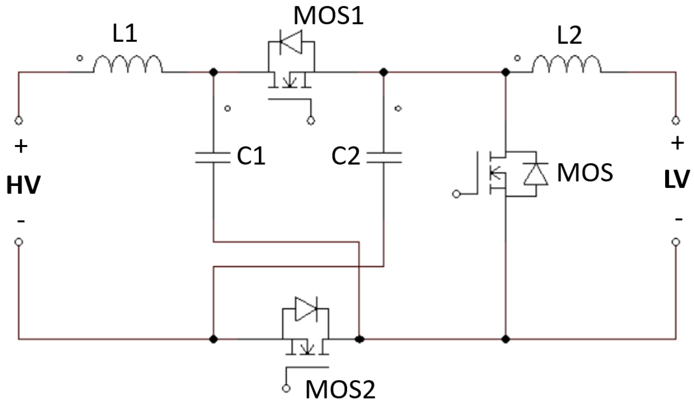
A schematic of the proposed DC-DC converter is shown in Figure 1. It consists of three switching devices (MOS1-MOS2-MOS), two inductors (L1–L2), and two capacitors (C1–C2). The presented DC-DC converter is able to work according to a buck-boost operation, meaning that, according to the energy flow direction, it can work in either in step-down (buck) or in step-up (boost) operation: in the buck operation, the high voltage (HV) is the source and the low voltage (LV) is the load, whereas in the step-up operation, the energy flows in the opposite direction.
In Table 1, the main intended specifications are given in terms of the HV and LV voltages VHV and VLV, target power level P, maximum current ripple on HV and LV sides (ΔIL1,max and ΔIL2,max respectively), power density, and maximum desired power losses.
Based on pulse-width modulation (PWM) control, the power flow amount and direction can be regulated according to the duration of the on and off states of the MOSFETs: when MOS1 and MOS2 are on (during Ton), MOS is off, and vice versa (during Toff). This topology is quite simple if the corresponding unidirectional configuration is considered, where the active switches MOS1 and MOS2 are replaced by two diodes and the only active switch is MOS. Furthermore, due to the use of bidirectional switches, the direction of the current on the inductors can also be reversed, so that the converter is in continuous conduction mode (CCM) in any condition. As for the current ripple at the input and output sections, this is inherently low in the proposed converter since this topology is based on two inductances at both the terminal sections, leading to a current that does not pulsate. This implies the need of external filtering networks that are not bulky, limited electromagnetic emissions, and a reduction in the ripple of the input and output voltages.
2.1. Step-Down Operation
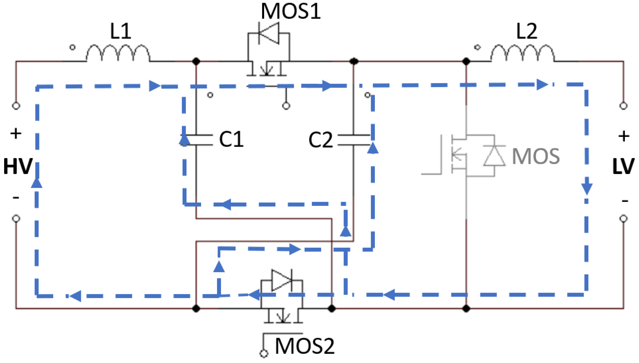
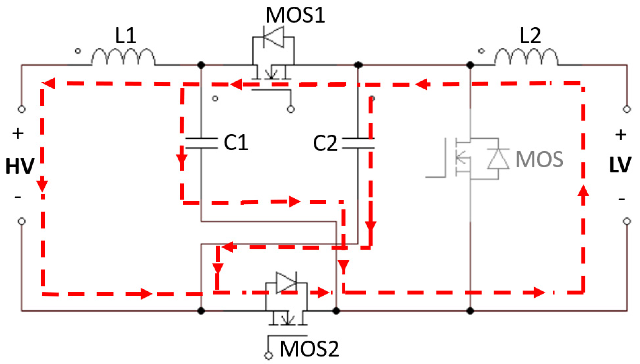
In Figure 2 and Figure 3, the proposed converter is shown in its two operating modes regarding the step-down configuration, corresponding to the periods Ton and Toff, respectively, and referenced as Mode 1 and Mode 2. Inside the switching Ts period, Ton and Toff are the subperiods when MOS1 and MOS2 are on and off, respectively. Notably, according to the switched-capacitor structure, the connection between C1 and C2 changes from parallel in Mode 1 to series in Mode 2.
By assuming that VC1 = VC2 in both operating modes, since C1 and C2 are considered identical, and according to the Kirchhoff laws, as known from circuits theory, the following equations arise:
During Mode 1:
During Mode 2:
According to the energy balance regarding inductors L1 and L2 in a steady-state condition and according to the previous equations, the following expressions are obtained:
According to (6), the following equation regarding capacitor voltage arises:
The duty cycle D is defined as follows:
The switching period can be defined as:
Therefore, according to (7)–(9):
By substituting (10) into (5), the following equation is obtained:
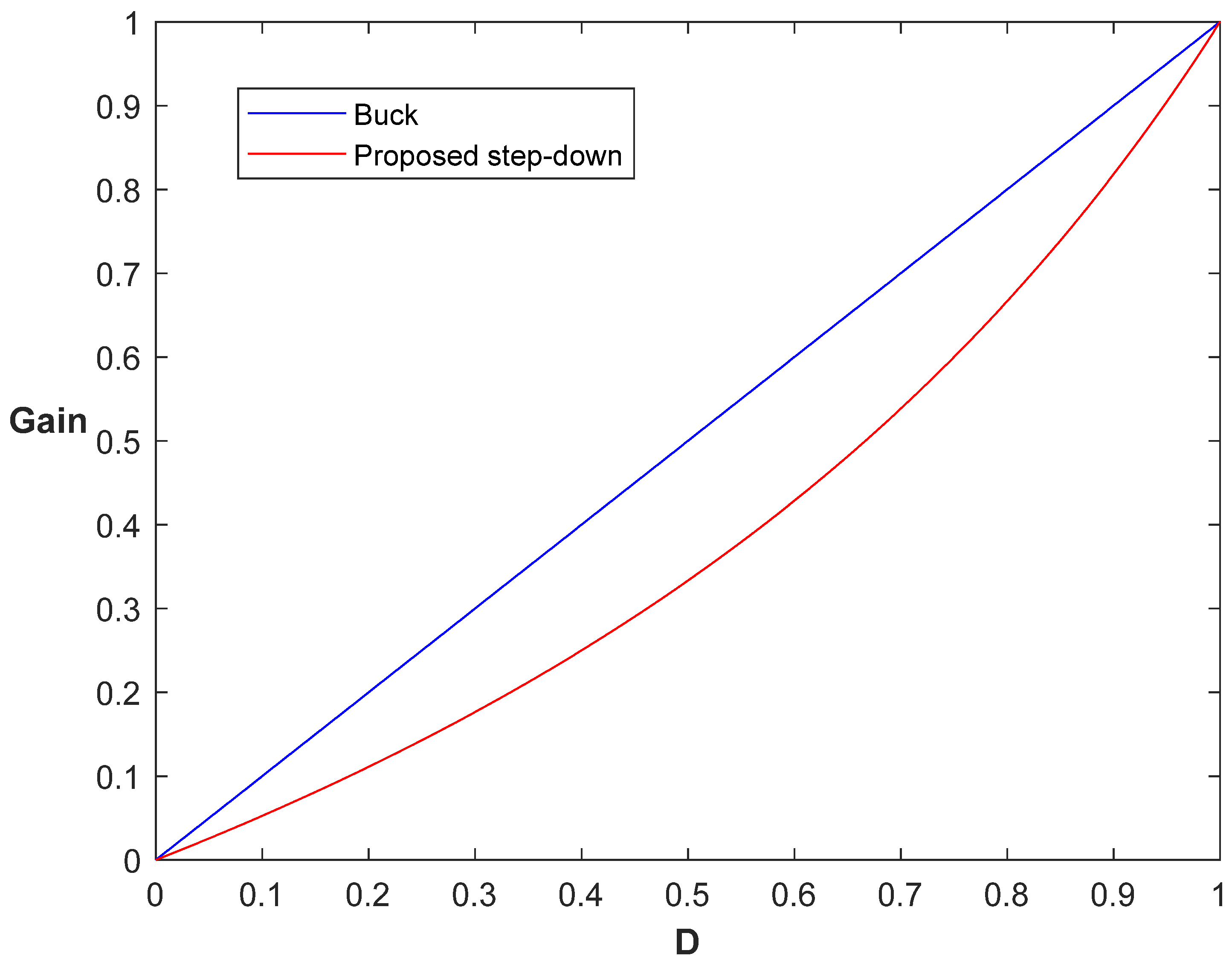
Finally, the load-to-source voltage gain can be derived as:
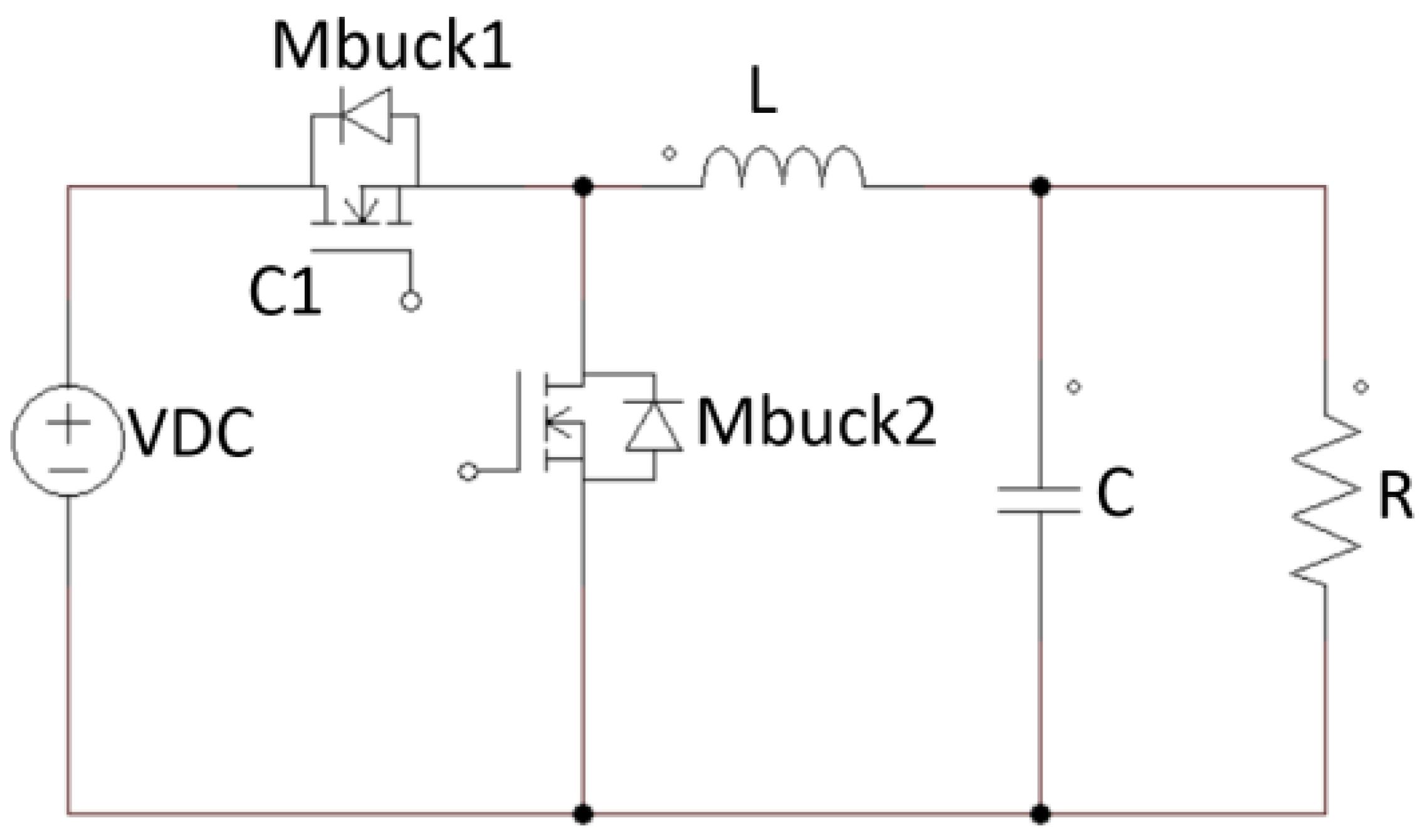
In Figure 4, a schematic of a conventional buck converter is shown.
Assuming that in this switching converter, Ton and Toff refer to the switch Mbuck1, the following load-to-source gain is derived, as is well known:
According to (12) and (13), in Figure 5, the ideal conversion ratio of the output voltage to the input voltage for the proposed converter in step-down mode is shown as a function of the duty cycle, and compared to the conventional buck converter gain.
2.2. Step-Up Operation
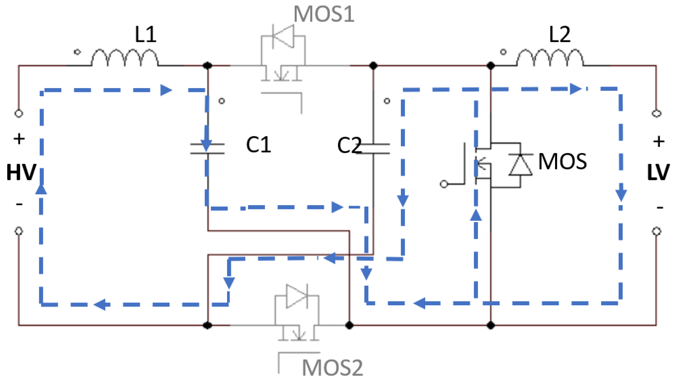
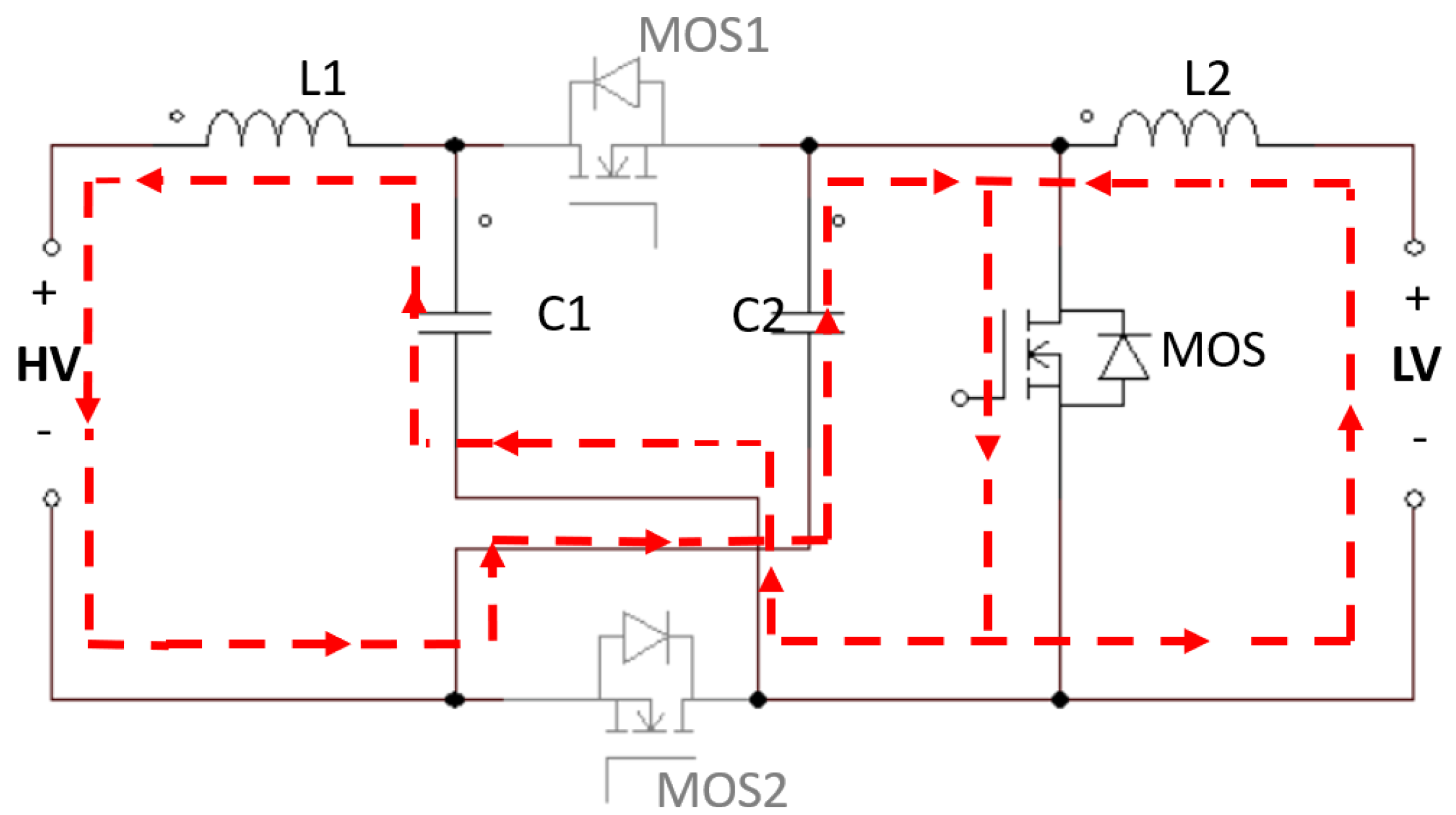
In Figure 6 and Figure 7, the proposed converter is shown in its two operating modes regarding the step-up configuration.
In the same way as in the step-down case, a system of proper equations can also be gained for the step-up operation, thus obtaining the ideal conversion ratio, as in the following:
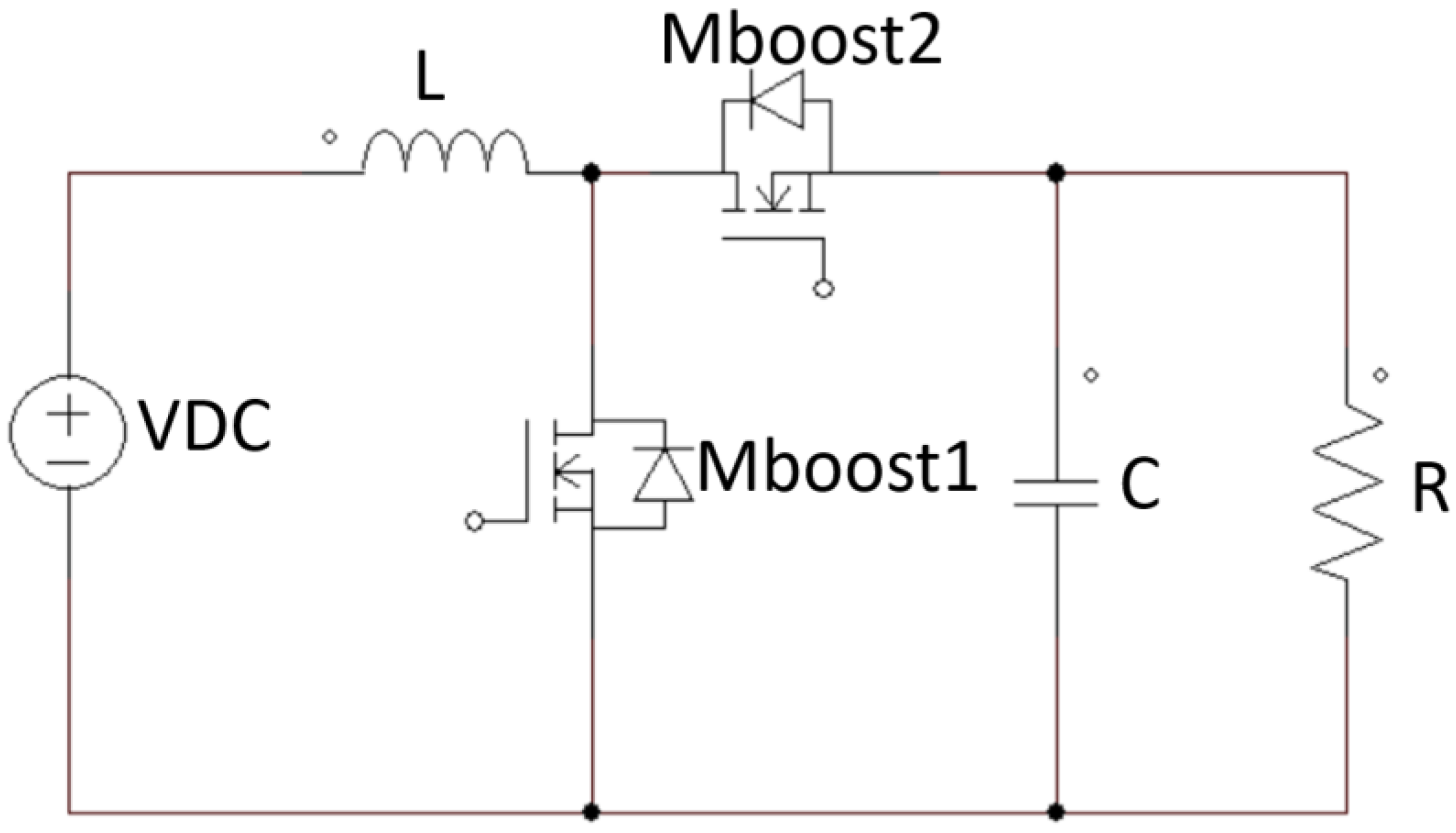
In Figure 8, a schematic of a conventional boost converter is shown.
Assuming that in this switching converter, Ton and Toff refer to the switch Mboost1, the following load-to-source is derived, as is well known:
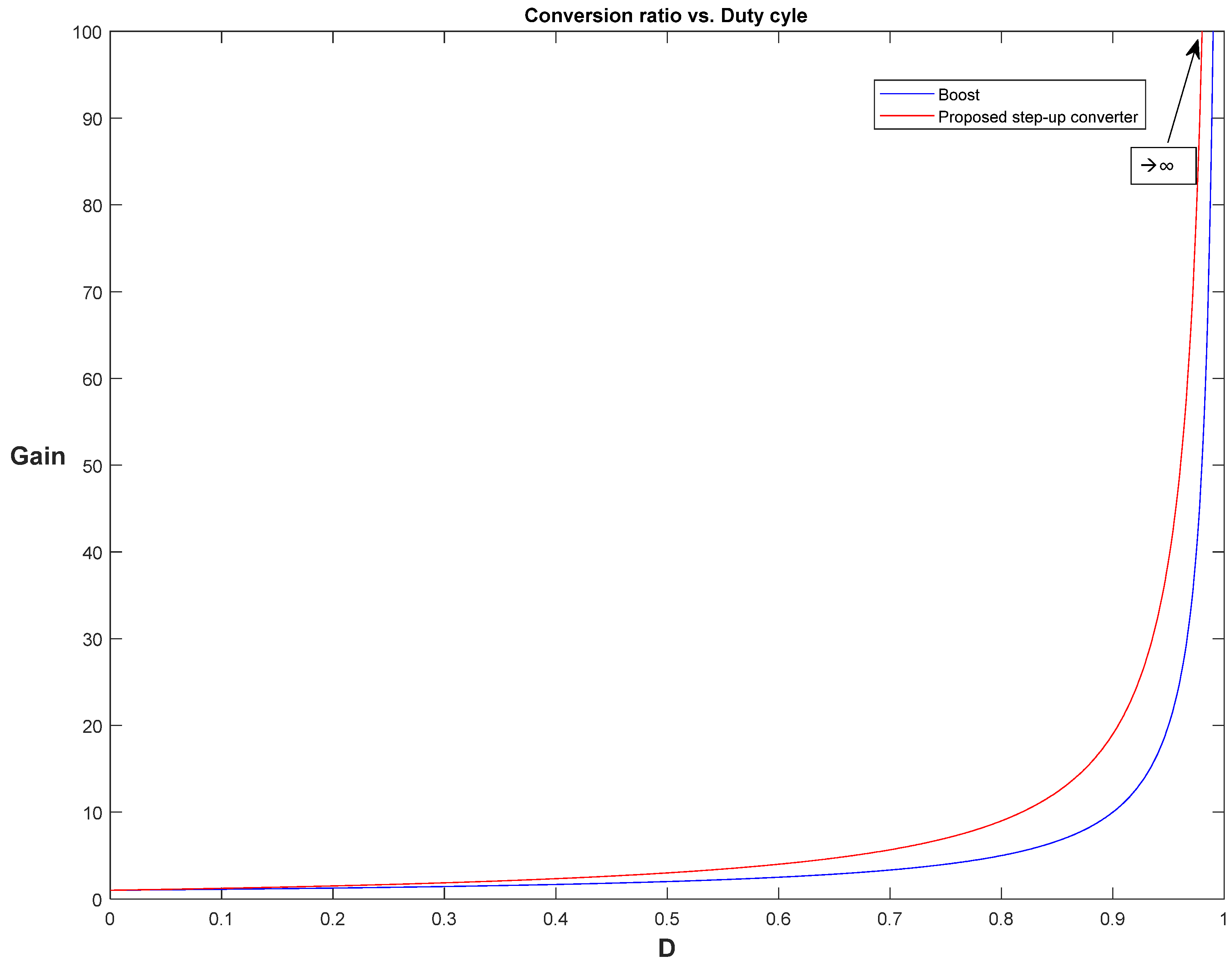
According to (14) and (15), in Figure 9, the ideal conversion ratio of the output voltage to the input voltage for the proposed converter in step-up mode is shown as a function of the duty cycle, and compared to the conventional boost converter gain. In this case, the duty cycle of the proposed converter has been referred to the switch MOS in order to obtain a gain increase along with the duty cycle increase.
2.3. Steady-State Current Analysis and Voltage Stress across the Components
Regarding the current waveforms, the following equations arise, both in step-down and step-up operations:
During Mode 1:
Therefore:
During Mode 2:
A proper investigation into the voltage stress across the single components should be performed in order to choose them correctly. According to Equations (1)–(4), the maximum voltage stress on each inductor can be obtained. Based on (1), (3), and (10), the voltage across L1 during Mode 1 and Mode 2 is:
During Mode 1:
During Mode 2:
According to (12), from (13) and (14) the following arise:
During Mode 1:
During Mode 2:
Based on (2), (4), and (10), the voltage across L2 during Mode 1 and Mode 2 is:
During Mode 1:
During Mode 2:
According to (12), from (17) and (18) the following arise:
During Mode 1:
During Mode 2:
Considering the results of Equations (15), (16), (19) and (20), the voltage across the inductors is the same:
Therefore, according to (19)–(21), the maximum voltage stress on each inductor is equal to VHV. Regarding the voltage across the switches, the maximum voltage stress occurs when in interdiction; therefore, during Mode 1 for MOS and during Mode 2 for MOS1 and MOS2:
During Mode 1:
During Mode 2:
Therefore, the maximum voltage stress on the switches arises:
3. Design of the Proposed Switched-Capacitor Converter
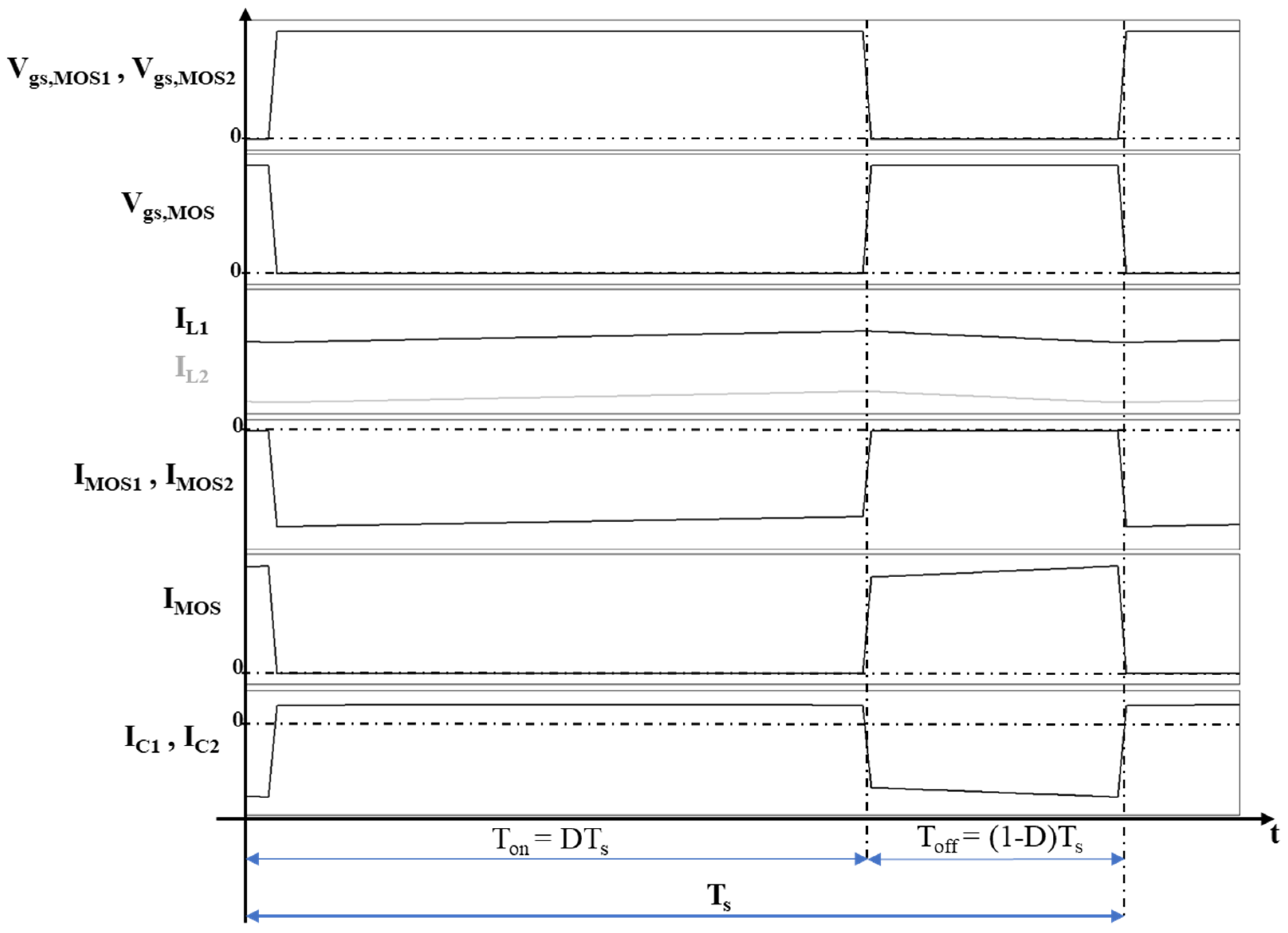
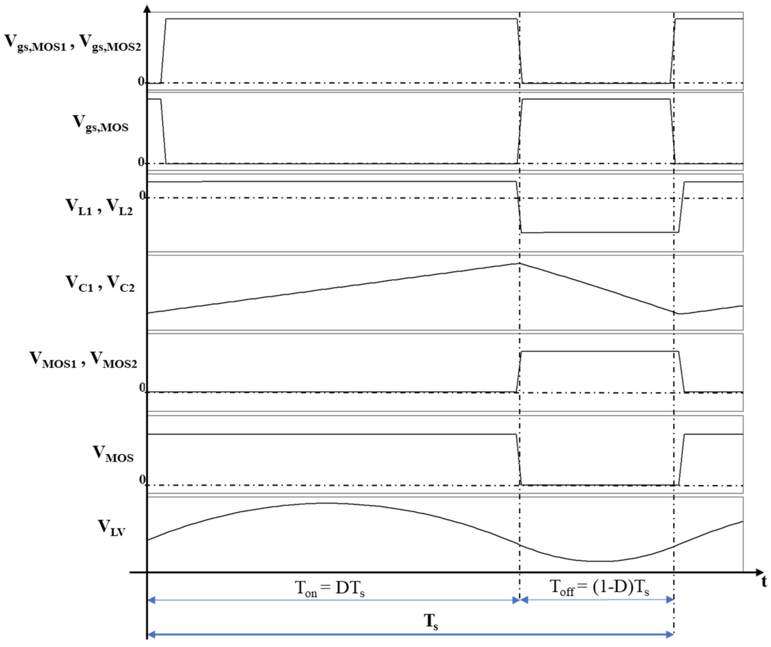
In Figure 10 and Figure 11, the main waveforms of the proposed converter are highlighted in order to show its behavior.
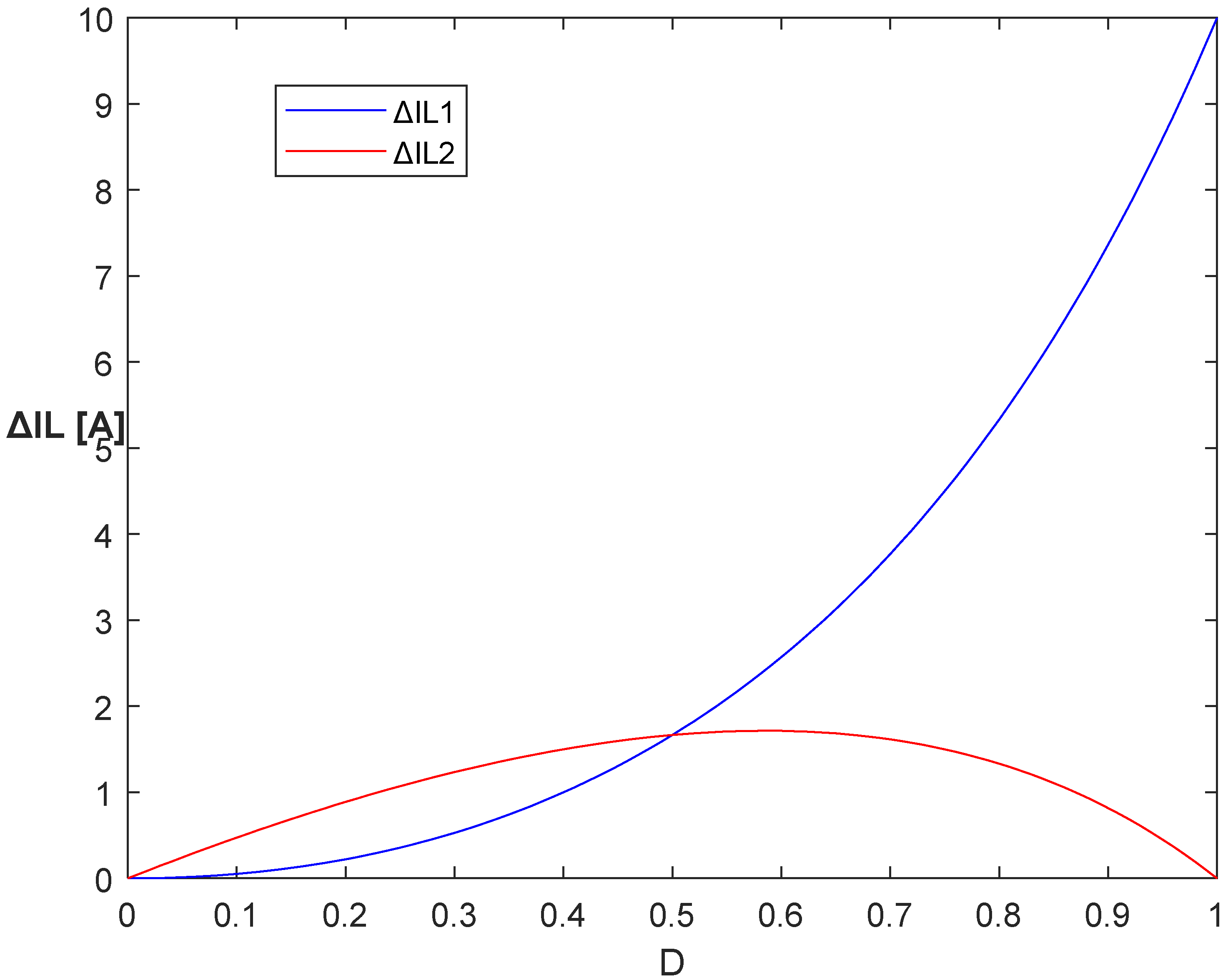
The maximum current ripple and maximum voltage ripple were considered as the design criteria to size the inductances and capacitances, respectively. The ripples of current ΔIL1 and ΔIL2 can be obtained by considering either the Ton (Mode 1) or the Toff (Mode 2). If Mode 1 is considered, then:
Therefore:
The maximum desired current ripple can be considered as a design criterion in order to size inductances. If a maximum 10 A value is defined for the current ripple, considering a case of a switching frequency fs equal to 400 kHz, L1 and L2 are sized equal to 100 μH. The corresponding values of the current ripple are reported in Figure 12.
The ripples of voltage ΔVC1 and ΔVC2 can be obtained by considering either the Ton (Mode 1) or the Toff (Mode 2). If Mode 2 is considered, then:
Therefore:
The maximum desired voltage ripple can be considered as a design criterion in order to size the capacitances. If a maximum 2.5 V value is defined for voltage ripple, considering a case of a switching frequency fs equal to 400 kHz and a pessimistic case of L1 average current equal to 1000 A, C1 and C2 are sized equal to 1000 μF. Correspondingly, the voltage ripples follow a decreasing linear trend with respect to the duty cycle, starting from the maximum ripple of 2.5 V at D = 0.
The capacitance C is implemented through an electrolytic capacitor, whereas the capacitances C1 and C2 are realized by means of metallized polypropylene film capacitors. A more detailed description of possible components that can be accordingly used is given in the following paragraphs. The switching frequency value of 400 kHz was chosen as an example, supposing that at high frequency and high voltage levels, SiC switching devices are used.
The parameter values of the proposed converter are accordingly reported in Table 2.
4. Parasitic Effects on the Converter Gain
The convenience of the proposed configuration is highlighted by Figure 5 and Figure 9, since the input-to-output gain in the step-down operation and the output-to-input gain in the step-up operation are higher for any duty cycle.
Nevertheless, a proper comparison must also consider the parasitic elements of the real components, due to their power losses. In order to estimate the influence of the parasitic components on the steady-state behavior of the proposed converter, only the equivalent series resistances of the employed components were considered as parasitic elements. This is especially evident in the step-up configurations, for which the real gain declines as the duty cycle approaches zero.
Indeed, both in the conventional boost converter and in the proposed step-up configuration, no energy can supply the load if the duty cycle is zero. Therefore, a peak in the gain vs. duty cycle curve is present for an intermediate value of D.
Simulations in the PowerSIM environment of the proposed converter, according to the parameters reported in Table 2, were carried out in order to evaluate the feasibility of the production of a future prototype and to estimate the influence of the parasitic effects on the voltage gain. In the simulation, a simple model for MOSFETs was considered, consisting mainly in the conductive losses, due to the need to understand the general behavior of the proposed converter, without investigating in detail, in a preliminary phase of study, the switching transients.
Most of the power losses are concentrated in the series elements, which are the switches, the capacitors, and the inductors. Therefore, for each of these components, an equivalent resistance Rs was considered and, for the sake of simplicity, the Rs value was chosen to be identical for each of them. Furthermore, as reported in Table 3 two different cases of parasitic effects were investigated, corresponding to two different values of per-unit-resistance R*, defined as the ratio of Rs to the load resistance R: case (a) refers to an R* of 0.001; case (b) refers to an R* of 0.01. The conventional boost (conv. step-up) and the proposed converter in step-up operation (prop. step-up) were compared, considering open-loop simulations according to the values reported in Table 2, to a DC source voltage of 48 V and to a load resistance R of 10 Ω.
In Figure 13, Figure 14, Figure 15 and Figure 16, the main waveforms in terms of gate signals, output voltage, and inductor currents regarding the proposed step-up and the conventional boost converter are provided with respect to both the considered cases of parasitic effects. The provided simulation plots refer to the maximum achieved gains. In more detail, Figure 13 and Figure 14 concern case (a), whereas Figure 15 and Figure 16 concern case (b), respectively.
5. Discussion
Based on the results reported above, the convenience of the proposed converter with respect to the conventional boost topology arises if the components are designed and produced to minimize power losses.
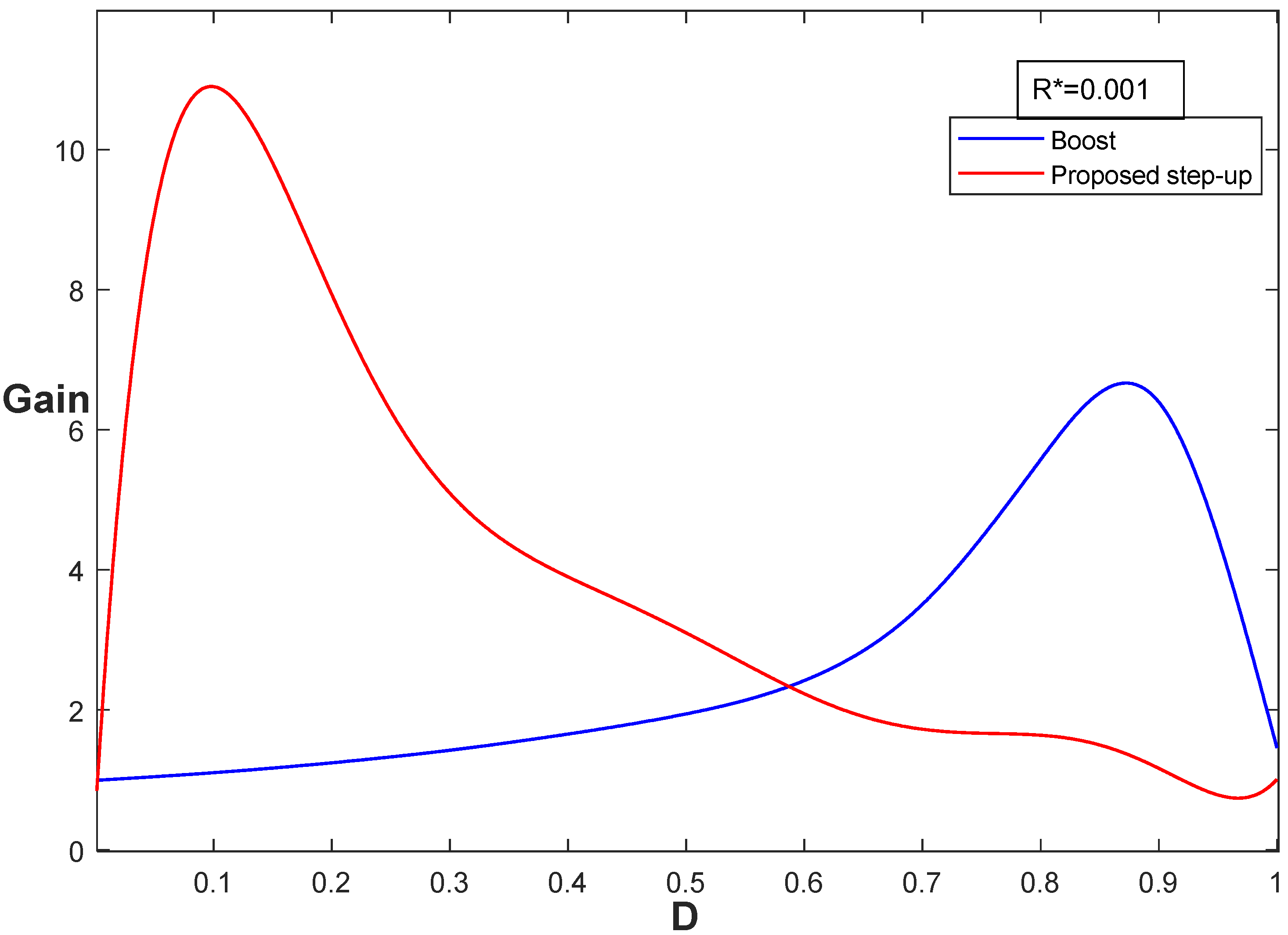
Therefore, it is crucial to select the devices and design the power converter so that the equivalent series resistances are minimized. Regarding this issue, case (a) in Table 3, which is the most challenging case in terms of power losses, is compliant with the equivalent series resistance (ESR) of some emerging switch and capacitor technologies. Silicon carbide (SiC) power MOSFETs [36] and metallized polypropylene film capacitors [37] compliant with the capacitance value in Table 2 guarantee very low ESRs at 600 V, equal to 12 mΩ and 1.7 mΩ, respectively. Attention should be paid to single electrolytic capacitors, since the higher the voltage rating, the higher the equivalent series resistance (ESR). Nevertheless, the higher the capacitance value, the lower the ESR; therefore, it is convenient to select a high-value electrolytic capacitor in order to minimize parasitic effects. For instance, given the capacitance value reported in Table 2, a maximum ESR of 143 mΩ was reported by a typical datasheet for a 400 V voltage [38], but if the value is decreased to 3600 µF, a maximum ESR of 43 mΩ is reported. Solutions based on the device’s parallel connection are particularly advantageous, offering a minimization of the equivalent series resistance even for the highest power levels. Indeed, a maximum voltage gain of more than 10 can be obtained from the proposed topology in case (a), which is more than compliant with the (400–48) V specification for the DC-DC converter.
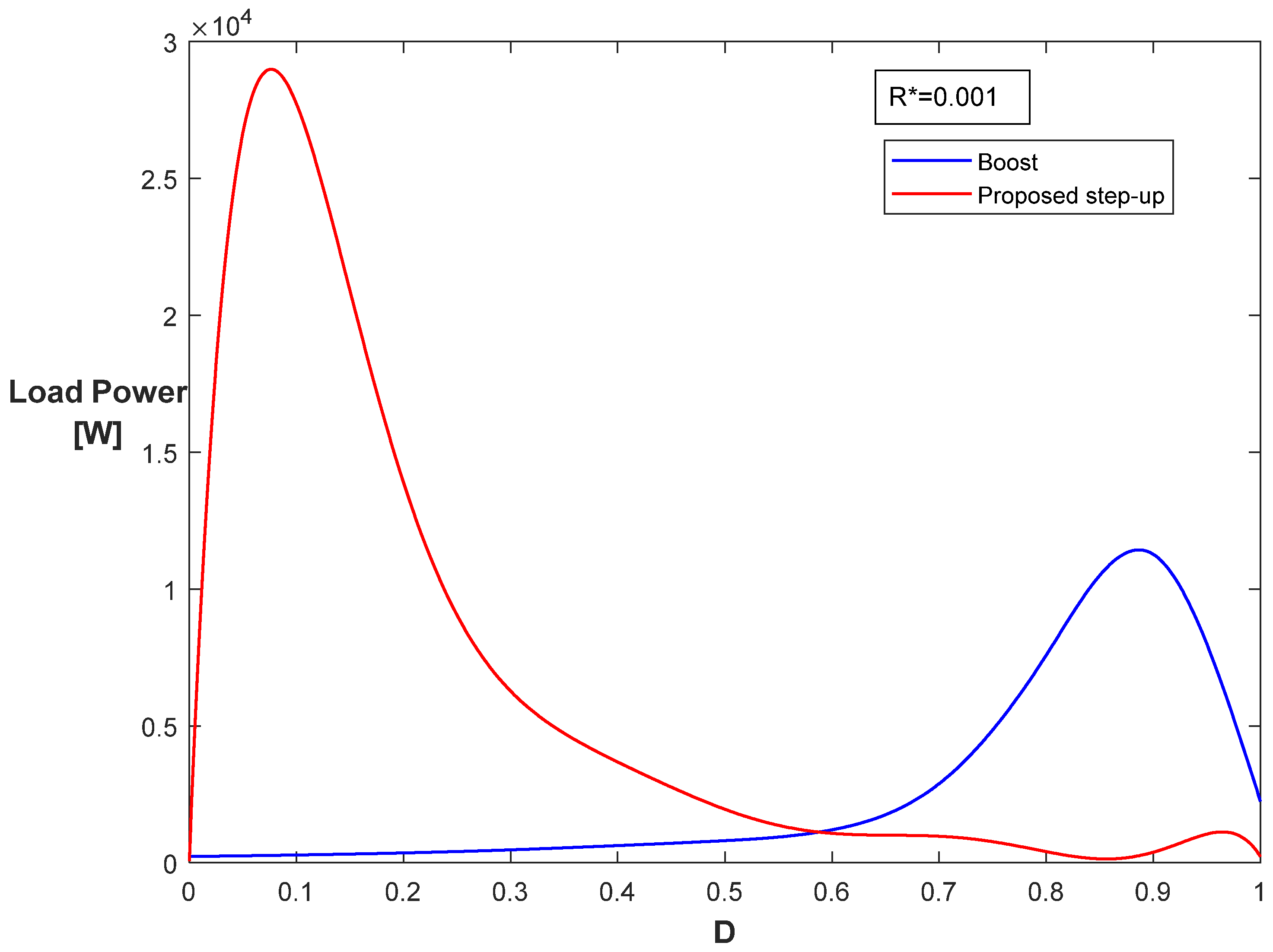
From the comparison between the given results, the proposed converter is able to supply a maximum power of almost 30 kW for a load resistor R of 10 Ω, whereas the maximum power supplied by the conventional topology is half of this, as highlighted in Figure 19. These data were obtained via simulation results post-processing, considering the open-loop step-up configuration with a source voltage of 48 V. For a duty cycle of about 0.1, the maximum power load was obtained, corresponding to a load voltage of about 547 V.
In automotive environments, the results achieved by the proposed converter represent a great advantage due to the need for high voltage ratios, e.g., between DC storage systems or between low-voltage battery packs and high-voltage electric motors, and for low electromagnetic disturbances without bulky and expensive filtering networks. Indeed, the presence of the series inductor inside the converter topology guarantees low current ripples.
The power efficiency at the maximum load power is 57% for R* = 0.001. This implies an input power of around 50 kW, equivalent to an average source current of 1000 A. Although this represents the worst case, it is required to parallelize devices in order to obtain a total maximum current rate of 1000 A. The power efficiency reaches at least 95% for load power values of less than 5 kW, since the lower the current, the lower the conduction losses. This is compliant with the specifications given in Table 1, reporting a 10% maximum value in terms of desired converter power losses.
The efficiency estimation was taken into account, in addition to the equivalent series resistances of the reactive components and the conduction losses of the switching devices. The switching losses were not considered because they are beyond the focus of this paper, even though a future efficiency analysis would be appropriate to better compare it to other topologies.
Table 4 reports the voltage rating of the devices according to (19)–(22) and (28)–(32), where a value of D equal to 0.1 was considered as the worst case, considering that under this value, the power load curve quickly reaches zero, as highlighted by Figure 19.
Although power transfer efficiency is an issue beyond the focus of this paper, future developments of the proposed circuit involve improvements in order to guarantee high levels of efficiency, even for the highest voltage and power levels, as required by automotive applications. Capacitor soft-charging capability is possibly needed for this purpose, so that hard switching power losses generally occurring in switching capacitor-based converters can be properly smoothed.
As far as the transistor selection is concerned, a derating factor of half its rated maximum voltage is suggested as a design safety margin. Furthermore, snubber networks are recommended to smooth over voltages due to inductive parasitic elements.
An investigation of switching losses with respect to the switching frequency will be crucial to better evaluate the behavior in real applications, as well as considering emerging technologies in switching semiconductor devices.
6. Conclusions
In this paper, a bidirectional DC-DC converter for the management of a storage system is proposed. One of the most important fields in which electrical storage systems are applied is electric mobility.
In the context of an electric vehicle (EV), the on-board power system architecture can include a high-voltage primary source and a low-voltage section, represented by a DC voltage bus or a storage system.
The main goal of this study was to present an innovative bidirectional DC-DC converter interconnecting a 400 V battery and a 48 V DC section. The proposed converter features low electromagnetic emissions due to the series inductors at the input and output sections, thus minimizing current ripples, and low complexity with respect to other high-gain topologies.
Specifically, a non-isolated converter was selected and investigated, in order to avoid the bulky and expensive implications of using a transformer.
After a deep steady-state analysis of the converter, the main electrical waveforms were presented in order to depict the circuit behavior. Design considerations regarding the sizing of reactive components and the current and voltage rating of switching devices were also provided.
The presented simulation results, arising from the software tool PowerSIM, highlight the convenience of the proposed topology in terms of voltage gain with respect to the conventional buck-boost converter, as well as considering the influence of parasitic effects. The results prove the feasibility of an experimental realization, reaching a maximum power level of 30 kW, which is double that reached in the conventional topology.
Furthermore, with respect to other non-isolated converters with higher gain than conventional buck or boost converters, particularly the switched-capacitor converters to which it belongs, the proposed converter provides an optimal trade-off between complexity and electromagnetic emissions, as well as offering the possibility of bidirectional operation.
Author Contributions
Conceptualization, F.P. and C.P.; methodology, V.D.D.; software, C.P. and F.P.; validation, R.M. and F.P.; formal analysis, F.P. and C.P.; investigation, F.P.; resources, V.D.D.; data curation, R.M. and C.P.; writing—original draft preparation, F.P.; writing—review and editing, R.M. and V.D.D.; visualization, C.P.; supervision, R.M.; project administration, V.D.D. and R.M.; funding acquisition, V.D.D. All authors have read and agreed to the published version of the manuscript.
Funding
This work was produced with financial support from the following grants: the European Union PO FESR Sicilia 2014–2020, Action 1.1.5, Project n. 08000PA90246, Project title: “Smart grids per le isole minori (Smart grids for small islands)”, acronym: I-Sole CUP G99J18000540007; PON R&I 2015–2020 PROpulsione e Sistemi IBridi per velivoli ad ala fifissa e rotante PROSIB, CUP no: B66C18000290005; PRIN 2017, Advanced power-trains and -systems for full electric aircrafts, prot. no.: 2017MS9F49; PON R&I 2014–2020—AIM (Attraction and International Mobility), project AIM1851228-1. The paper’s content is the responsibility of the authors and it does not necessarily reflect the point of view of the European Union. The authors would like to thank Layer Electronics Srl for their assistance during on-field tests and the availability of the test site.
Conflicts of Interest
The authors declare no conflict of interest.
References
- Di Dio, V.; Miceli, R.; Rando, C.; Zizzo, G. Dynamics photovoltaic generators: Technical aspects and economical valuation. In Proceedings of the International Symposium on Power Electronics, Electrical Drives, Automation and Motion (SPEEDAM), IEEE, Pisa, Italy, 14–16 June 2010; pp. 635–640. [Google Scholar]
- Cecconi, V.; Di Dio, V.; Di Tommaso, A.O.; Di Tommaso, S.; La Cascia, D.; Miceli, R. Active power maximizing for Wind Electrical Energy Generating Systems moved by a Modular Multiple Blade Fixed Pitch Wind Turbine. In Proceedings of the 2008 International Symposium on Power Electronics, Electrical Drives, Automation and Motion, Ischia, Italy, 11–13 June 2008; pp. 1460–1465. [Google Scholar]
- Cipriani, G.; Di Dio, V.; Madonia, N.; Miceli, R.; Pellitteri, F.; Galluzzo, F.R. Reconfiguration strategies to reduce mismatch effects on PV array: An Arduino-based prototype. In Proceedings of the 2014 International Symposium on Power Electronics, Electrical Drives, Automation and Motion, Ischia, Italy, 18–20 June 2014; pp. 1003–1008. [Google Scholar]
- Livreri, P.; Castiglia, V.; Pellitteri, F.; Miceli, R. Design of a Battery/Ultracapacitor Energy Storage System for Electric Vehicle Applications. In Proceedings of the 2018 IEEE 4th International Forum on Research and Technology for Society and Industry (RTSI), Palermo, Italy, 10–13 September 2018; pp. 1–5. [Google Scholar]
- Castiglia, V.; Livreri, P.; Miceli, R.; Pellitteri, F.; Schettino, G.; Viola, F. Power Management of a Battery/Supercapacitor System for E-Mobility Applications. In Proceedings of the 2019 AEIT International Conference of Electrical and Electronic Technologies for Automotive (AEIT AUTOMOTIVE), IEEE, Turin, Italy, 2–4 July 2019; pp. 1–5. [Google Scholar]
- Ala, G.; Di Filippo, G.; Viola, F.; Giglia, G.; Imburgia, A.; Romano, P.; Castiglia, V.; Pellitteri, F.; Schettino, G.; Miceli, R. Different Scenarios of Electric Mobility: Current Situation and Possible Future Developments of Fuel Cell Vehicles in Italy. Sustainability 2020, 12, 564. [Google Scholar] [CrossRef] [Green Version]
- Pellitteri, F.; Boscaino, V.; Di Tommaso, A.O.; Miceli, R. Efficiency optimization in bi-directional inductive power transfer systems. In Proceedings of the 2015 International Conference on Electrical Systems for Aircraft, Railway, Ship Propulsion and Road Vehicles (ESARS), Aachen, Germany, 3–5 March 2015; pp. 1–6. [Google Scholar]
- Liu, C.; Chau, K.T.; Wu, D.; Gao, S. Opportunities and Challenges of Vehicle-to-Home, Vehicle-to-Vehicle, and Vehicle-to-Grid Technologies. Proc. IEEE 2013, 101, 2409–2427. [Google Scholar] [CrossRef] [Green Version]
- Sami, I.; Ullah, Z.; Salman, K.; Hussain, I.; Ali, S.M.; Khan, B.; Mehmood, C.A.; Farid, U. A Bidirectional Interactive Electric Vehicles Operation Modes: Vehicle-to-Grid (V2G) and Grid-to-Vehicle (G2V) Variations within Smart Grid. In Proceedings of the 2019 International Conference on Engineering and Emerging Technologies (ICEET), Lahore, Pakistan, 21–22 February 2019; pp. 1–6. [Google Scholar]
- Fathy, K.; Morimoto, K.; Doi, T.; Lee, H.W.; Nakaoka, M. An Asymmetrical Switched Capacitor and Lossless Inductor Quasi-Resonant Snubber-Assisted ZCS-PWM DC-DC Converter with High frequency Link. In Proceedings of the CES/IEEE 5th International Power Electronics and Motion Control Conference, Shanghai, China, 14–16 August 2006; pp. 1–5. [Google Scholar]
- Wu, T.-F.; Yang, J.-G.; Kuo, C.-L.; Wu, Y.-C. Soft-Switching Bidirectional Isolated Full-Bridge Converter with Active and Passive Snubbers. IEEE Trans. Ind. Electron. 2013, 61, 1368–1376. [Google Scholar] [CrossRef]
- Goyal, V.K.; Shukla, A. Isolated DC–DC Boost Converter for Wide Input Voltage Range and Wide Load Range Applications. IEEE Trans. Ind. Electron. 2020, 68, 9527–9539. [Google Scholar] [CrossRef]
- Matsumori, H.; Kosaka, T.; Sekido, K.; Kim, K.; Egawa, T.; Matsui, N. Isolated DC-DC Converter utilizing GaN power device for Automotive Application. In Proceedings of the 2019 IEEE Applied Power Electronics Conference and Exposition (APEC), Houston, TX, USA, 20–24 March 2019; pp. 1704–1709. [Google Scholar]
- Bastos, G.H.D.A.; Costa, L.F.; Tofoli, F.L.; Bascope, G.V.T.; Bascope, R.P.T. Nonisolated DC–DC Converters With Wide Conversion Range for High-Power Applications. IEEE J. Emerg. Sel. Top. Power Electron. 2019, 8, 749–760. [Google Scholar] [CrossRef]
- Kafle, Y.R.; Hasan, S.U.; Town, G. Quasi-Z-source based bidirectional DC-DC converter and its control strategy. Chin. J. Electr. Eng. 2019, 5, 1–9. [Google Scholar] [CrossRef]
- Tymerski, R.; Vorperian, V. Generation and classification of PWM DC-to-DC converters. IEEE Trans. Aerosp. Electron. Syst. 1988, 24, 743–754. [Google Scholar] [CrossRef]
- Leppäaho, J.; Suntio, T. Dynamic Characteristics of Current-Fed Superbuck Converter. IEEE Trans. Power Electron. 2010, 26, 200–209. [Google Scholar] [CrossRef]
- Sammaljärvi, T.; Lakhdari, F.; Karppanen, M.; Suntio, T. Modelling and dynamic characterisation of peak-current-mode-controlled superboost converter. IET Power Electron. 2008, 1, 527–536. [Google Scholar] [CrossRef]
- Gules, R.; Pfitscher, L.; Franco, L. An interleaved boost DC-DC converter with large conversion ratio. In Proceedings of the 2003 IEEE International Symposium on Industrial Electronics (Cat. No.03TH8692), Rio de Janeiro, Brazil, 9–11 June 2003; pp. 411–416. [Google Scholar]
- Zhang, G.; Zhang, B.; Li, Z.; Qiu, D.; Yang, L.; Halang, W.A. A 3-Z-Network Boost Converter. IEEE Trans. Ind. Electron. 2015, 62, 278–288. [Google Scholar] [CrossRef]
- Hsieh, Y.-P.; Chen, J.-F.; Yang, L.-S.; Wu, C.-Y.; Liu, W.-S. High-Conversion-Ratio Bidirectional DC–DC Converter With Coupled Inductor. IEEE Trans. Ind. Electron. 2013, 61, 210–222. [Google Scholar] [CrossRef]
- Liao, W.C.; Liang, T.J.; Liang, H.H.; Liao, H.K.; Yang, L.S.; Juang, K.C.; Chen, J.F. Study and implementation of a novel bidirectional DC-DC converter with high conversion ratio. In Proceedings of the Energy Conversion Congress and Exposition (ECCE), IEEE, Phoenix, AZ, USA, 17–22 September 2011; pp. 134–140. [Google Scholar]
- Jyotheeswara, R.K.; Sudhakar, N. High Voltage Gain Switched Capacitor Boost Converter with ANFIS Controller for Fuel Cell Electric Vehicle Applications. In Proceedings of the International Conference on Power Electronics, Intelligent Control and Energy Systems (ICPEICES), IEEE, New Delhi, India, 22–24 October 2018; pp. 465–470. [Google Scholar]
- Wu, G.; Ruan, X.; Ye, Z. Nonisolated High Step-Up DC–DC Converters Adopting Switched-Capacitor Cell. IEEE Trans. Ind. Electron. 2015, 62, 383–393. [Google Scholar] [CrossRef]
- Chauhan, A.K.; Raghuram, M.; Tripathi, A.K.; Singh, S.K.; Xiong, X.; Xuewei, P. A High Gain DC-DC Converter based on Switched Capacitor/Switched Inductor Arrangement. In Proceedings of the 2018 IEEE International Conference on Power Electronics, Drives and Energy Systems (PEDES), Chennai, India, 18–21 December 2018; pp. 1–6. [Google Scholar]
- Zhang, Y.; Gao, Y.; Zhou, L.; Sumner, M. A Switched-Capacitor Bidirectional DC–DC Converter With Wide Voltage Gain Range for Electric Vehicles With Hybrid Energy Sources. IEEE Trans. Power Electron. 2018, 33, 9459–9469. [Google Scholar] [CrossRef]
- Lee, Y.-S.; Chiu, Y.-Y. Zero-current-switching switched-capacitor bidirectional DC–DC converter. IEE Proc. Electr. Power Appl. 2005, 152, 1525–1530. [Google Scholar] [CrossRef] [Green Version]
- Axelrod, B.; Berkovich, Y.; Tapuchi, S.; Ioinovici, A. Single-Stage Single-Switch Switched-Capacitor Buck/Buck-Boost-Type Converter. IEEE Trans. Aerosp. Electron. Syst. 2009, 45, 419–430. [Google Scholar] [CrossRef]
- Biswas, I.; Kastha, D.; Bajpai, P. A Novel High Gain Switched Capacitor Topology for Fuel Cell Vehicles with Wide Voltage Gain. In Proceedings of the 2021 9th IEEE International Conference on Power Systems (ICPS), Kharagpur, India, 16–18 December 2021; pp. 1–6. [Google Scholar]
- Thota, P.R.; Jeevananthan, S. A New Switched Capacitor Nine-Level Inverter with Quadruple Voltage Boosting and Capacitor Voltage Balancing Capabilities. In Proceedings of the 2020 IEEE International Conference on Power Electronics, Drives and Energy Systems (PEDES), Jaipur, India, 16–19 December 2020; pp. 1–5. [Google Scholar]
- Salehian, A.; Hashemi, S.S.; Beiranvand, R.; Yazdian, A. Simulation of a Step-up Resonant Switched-Capacitor Converter under the CCM Operation Mode. In Proceedings of the 2019 10th International Power Electronics, Drive Systems and Technologies Conference (PEDSTC), Fars, Iran, 12–14 February 2019; pp. 230–235. [Google Scholar]
- Xu, J.; Gu, L.; Rivas-Davila, J. Effect of Class 2 Ceramic Capacitor Variations on Switched-Capacitor and Resonant Switched-Capacitor Converters. IEEE J. Emerg. Sel. Top. Power Electron. 2019, 8, 2268–2275. [Google Scholar] [CrossRef]
- Birtek, G.; Yildiz, A.B. Analysis of Switched Capacitor Circuits Based on Unified Ideal Switch Model. In Proceedings of the 2020 2nd Global Power, Energy and Communication Conference (GPECOM), Izmar, Turkey, 20–23 October 2020; pp. 98–101. [Google Scholar]
- Górecki, P.; Górecki, K. Analysis of the Usefulness Range of the Averaged Electrothermal Model of a Diode-Transistor Switch to Compute the Characteristics of the Boost Converter. Energies 2021, 14, 154. [Google Scholar] [CrossRef]
- Scognamillo, C.; Catalano, A.; Riccio, M.; D’Alessandro, V.; Codecasa, L.; Borghese, A.; Tripathi, R.; Castellazzi, A.; Breglio, G.; Irace, A. Compact Modeling of a 3.3 kV SiC MOSFET Power Module for Detailed Circuit-Level Electrothermal Simulations Including Parasitics. Energies 2021, 14, 4683. [Google Scholar] [CrossRef]
- SiC N-Channel MOSFET, 142 A, 650 V, 4-Pin TO-247 onsemi NTH4L015N065SC1-1. Available online: https://www.onsemi.com/products/discrete-power-modules/silicon-carbide-sic/silicon-carbide-sic-mosfets/nth4l015n065sc1 (accessed on 2 February 2022).
- KEMET C44U Polypropylene Film Capacitor, 600V dc, 10%, 1000μF, Screw Mount. Available online: https://content.kemet.com/datasheets/KEM_F3119_C44U_M.pdf (accessed on 2 February 2022).
- Snap-In Aluminum Electrolytic Capacitors. Available online: https://content.kemet.com/datasheets/KEM_A4081_ALC70.pdf (accessed on 2 February 2022).
Figure 1.
Schematic of the proposed switched-capacitor converter.

Figure 2.
The proposed converter in step-down operation: Mode 1.

Figure 3.
The proposed converter in step-down operation: Mode 2.

Figure 4.
Schematic of the conventional buck converter.

Figure 5.
Gain vs. duty cycle for conventional and proposed step-down converter.

Figure 6.
The proposed converter in step-up operation: Mode 1.

Figure 7.
The proposed converter in step-up operation: Mode 2.

Figure 8.
Schematic of the conventional boost converter.

Figure 9.
Gain vs. duty cycle for conventional and proposed step-up converter.

Figure 10.
The main current waveforms of the proposed converter during the switching period Ts.

Figure 11.
The main voltage waveforms of the proposed converter during the switching period Ts.

Figure 12.
Current ripple on L1 and L2 as function of the duty cycle D.

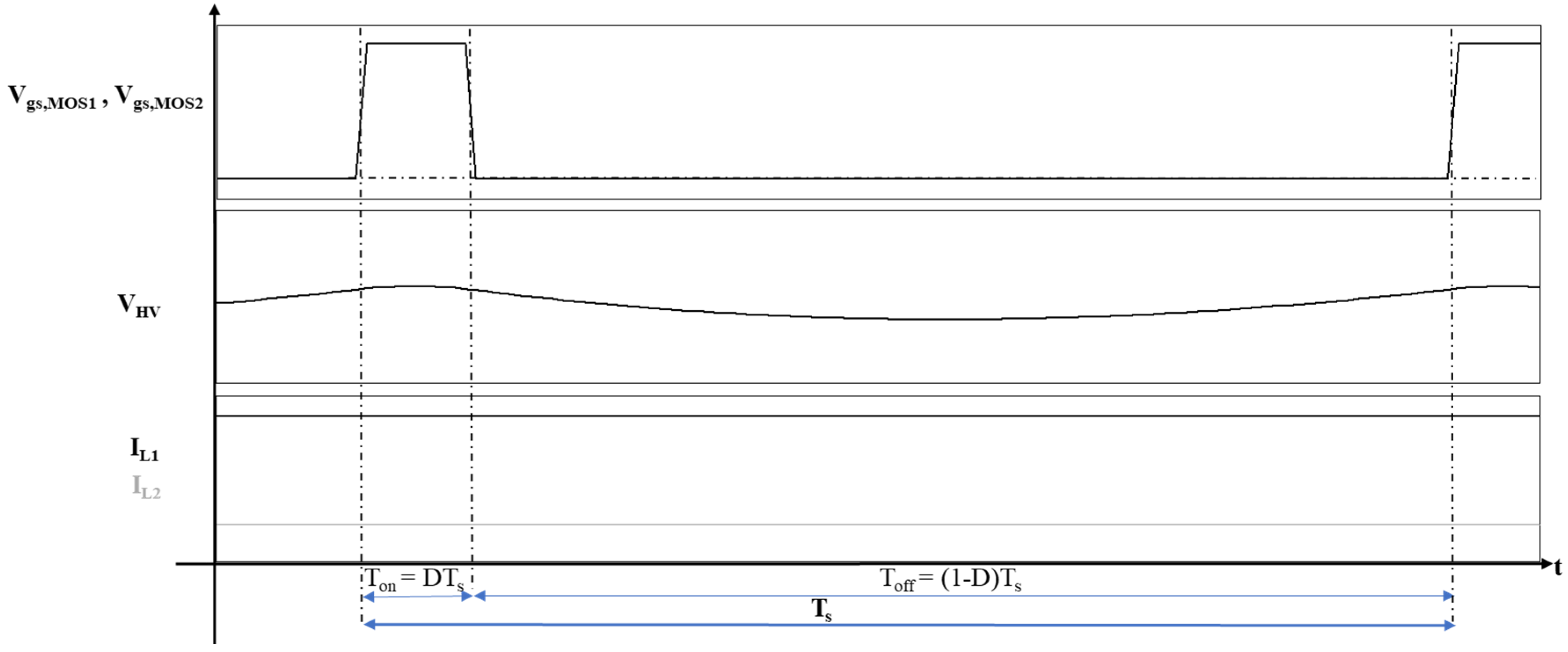
Figure 13.
Gate signals, output voltage, and inductor current waveforms of the proposed converter for case (a) at maximum achieved gain: VLV = 48 V; VHV = 528 V; D = 0.1.
Figure 13.
Gate signals, output voltage, and inductor current waveforms of the proposed converter for case (a) at maximum achieved gain: VLV = 48 V; VHV = 528 V; D = 0.1.

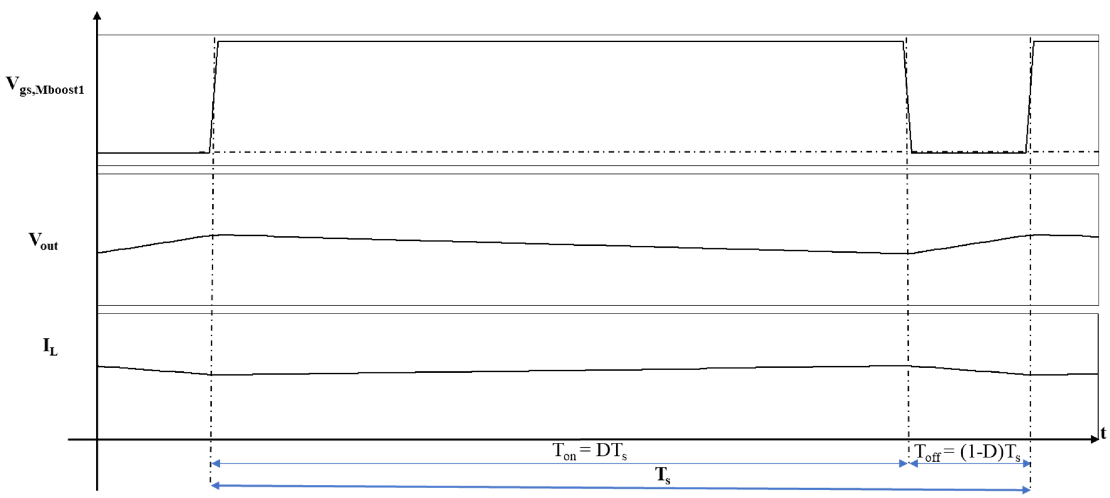
Figure 14.
Gate signal, output voltage, and inductor current waveforms of the conventional boost converter for case (a) at maximum achieved gain: Vin = 48 V; Vout = 297 V; D = 0.85.
Figure 14.
Gate signal, output voltage, and inductor current waveforms of the conventional boost converter for case (a) at maximum achieved gain: Vin = 48 V; Vout = 297 V; D = 0.85.

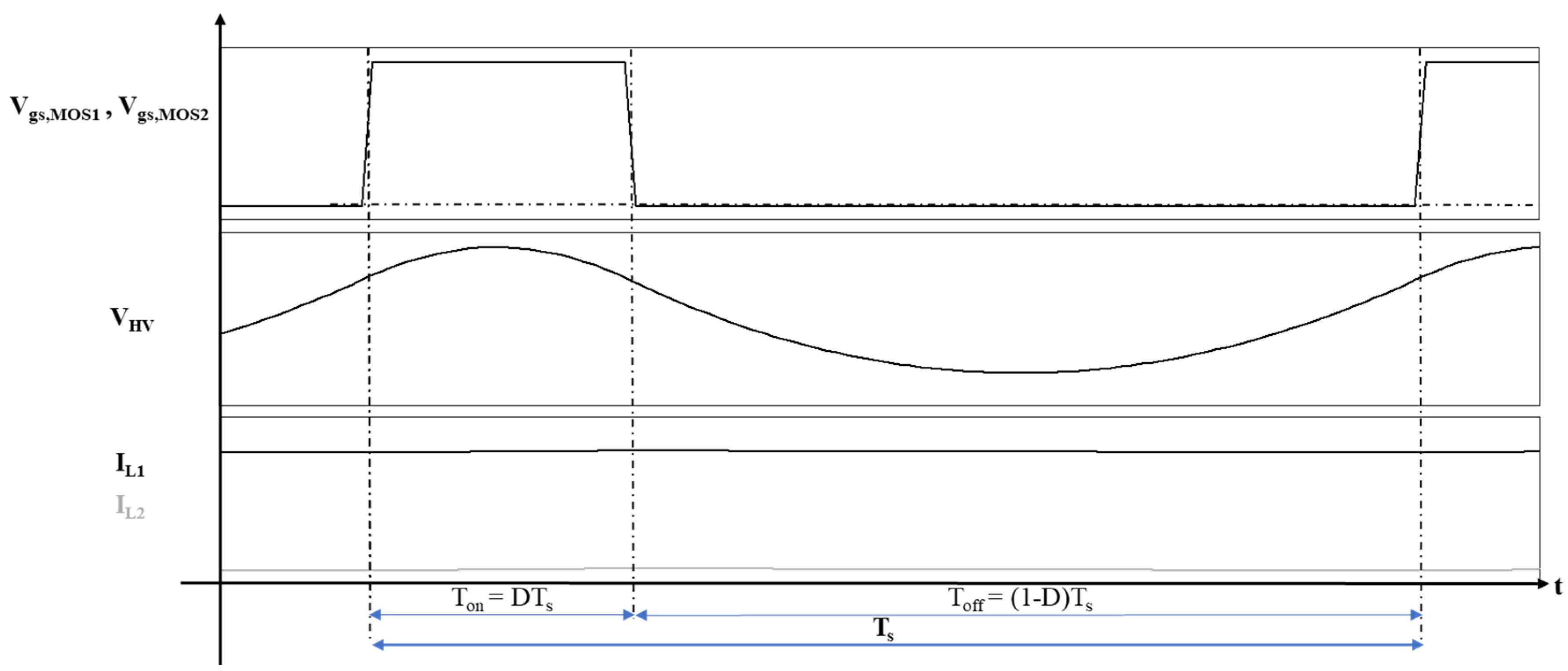
Figure 15.
Gate signals, output voltage, and inductor current waveforms of the proposed converter for case (b) at maximum achieved gain: VLV = 48 V; VHV = 170 V; D = 0.25.
Figure 15.
Gate signals, output voltage, and inductor current waveforms of the proposed converter for case (b) at maximum achieved gain: VLV = 48 V; VHV = 170 V; D = 0.25.

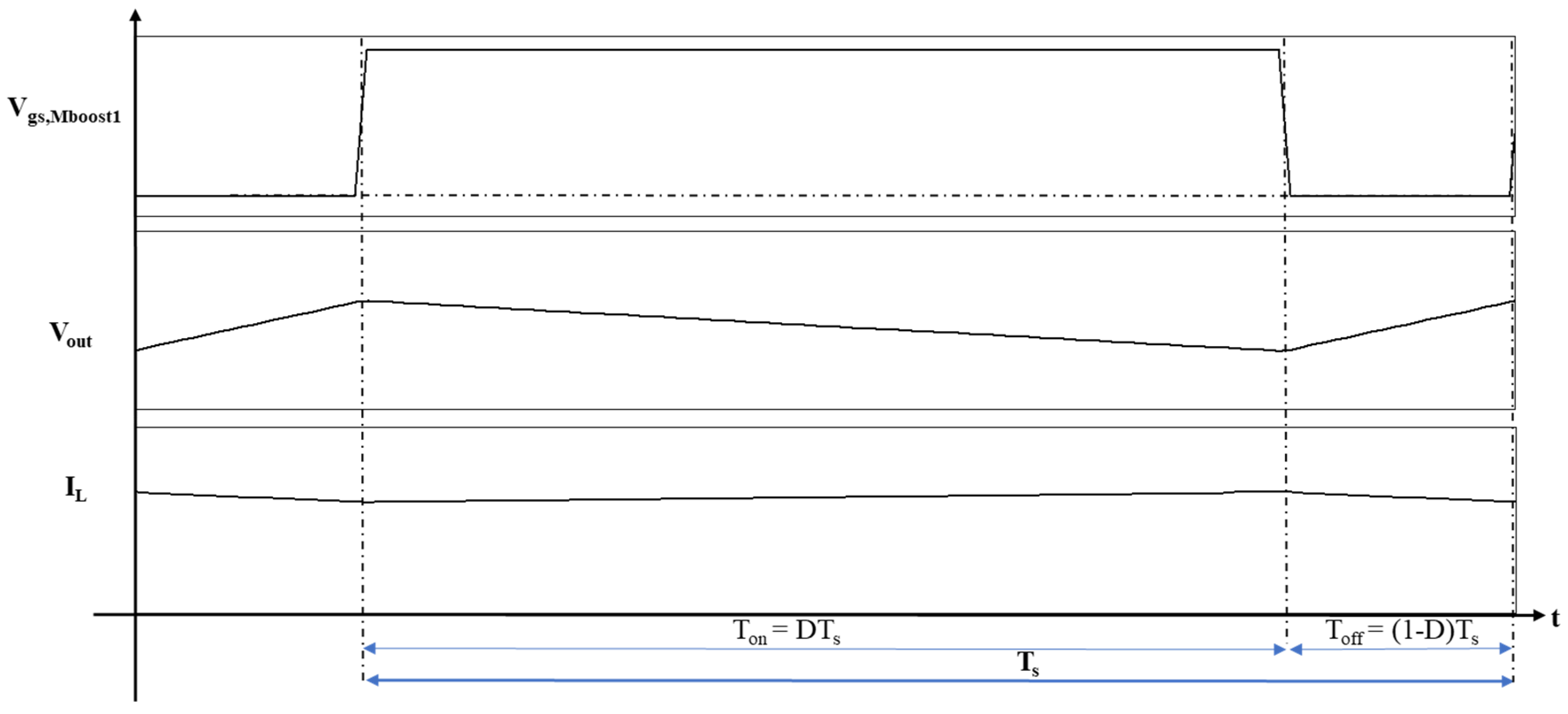
Figure 16.
Gate signal, output voltage, and inductor current waveforms of the conventional boost converter for case (b) at maximum achieved gain: Vin = 48 V; Vout = 165 V; D = 0.8.
Figure 16.
Gate signal, output voltage, and inductor current waveforms of the conventional boost converter for case (b) at maximum achieved gain: Vin = 48 V; Vout = 165 V; D = 0.8.

Figure 17.
Gain vs. duty cycle for conventional and proposed step-up converter for parasitic effects (a).
Figure 17.
Gain vs. duty cycle for conventional and proposed step-up converter for parasitic effects (a).

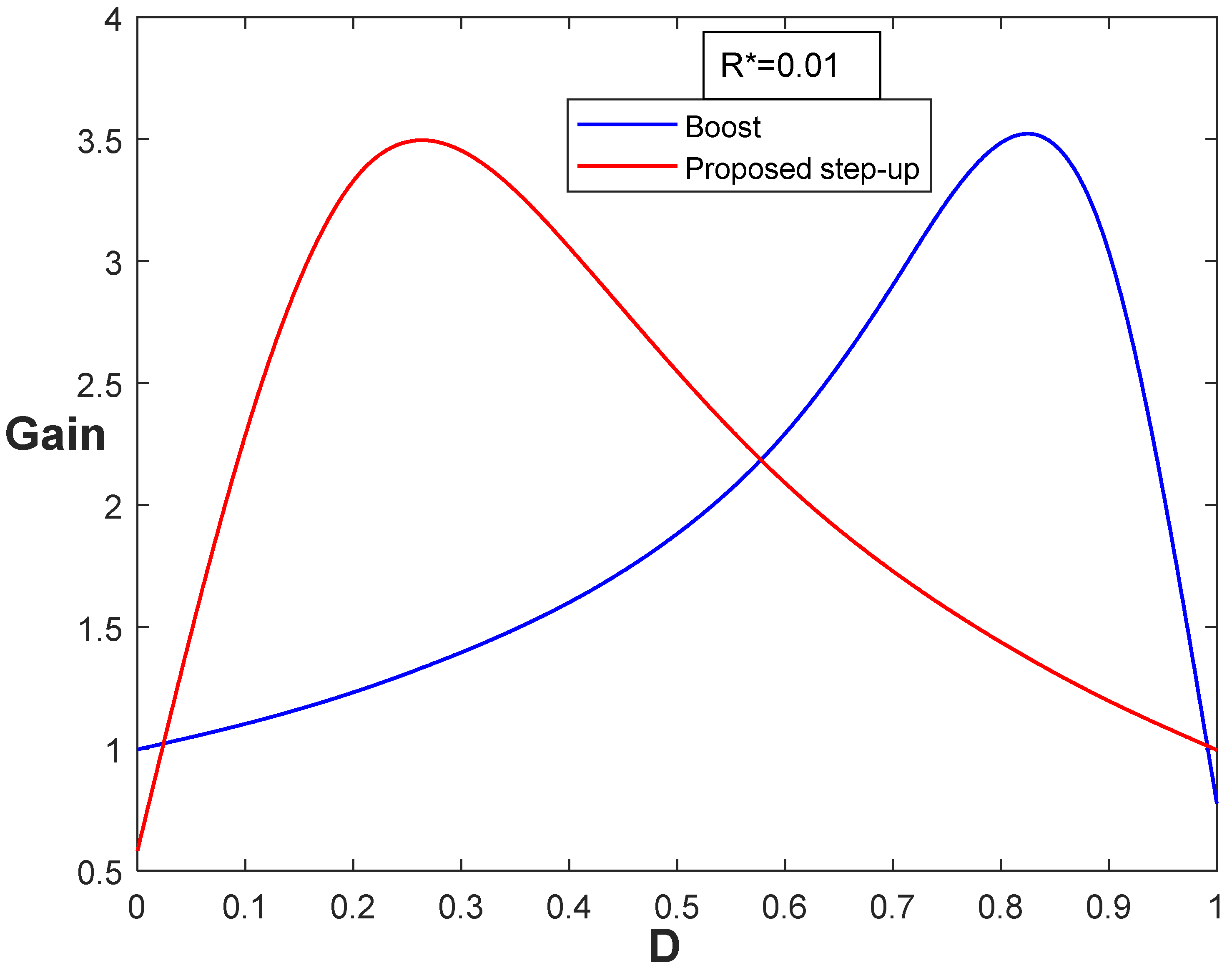
Figure 18.
Gain vs. duty cycle for conventional and proposed step-up converter for parasitic effects (b).
Figure 18.
Gain vs. duty cycle for conventional and proposed step-up converter for parasitic effects (b).

Figure 19.
Transferred power vs. duty cycle for conventional and proposed step-up converter for parasitic effects (a).
Figure 19.
Transferred power vs. duty cycle for conventional and proposed step-up converter for parasitic effects (a).


Table 1.
The converter specifications.
| Parameter | Value |
|---|---|
| VHV | 400 V |
| VLV | 48 V |
| P | 30 kW |
| ΔIL1,max = ΔIL2,max | 10 A |
| Power Density | 2 kW/kg |
| Max Power Losses | 10% |
Table 2.
The chosen parameters.
| C1 = C2 = C | L1 = L2 | fs |
|---|---|---|
| 1000 μF | 100 μH | 400 kHz |
Table 3.
Considered cases of parasitic effects.
| Case | Conv. Step-Up | Prop. Step-Up |
|---|---|---|
| Rs = Ron,MOS1 = Ron,MOS2 = RL | Rs = Ron,MOS1 = Ron,MOS2 = Ron,MOS = RL1 = RL2 = RC1 = RC2 | |
| (a) | R* = Rs/R = 0.001 | R* = Rs/R = 0.001 |
| (b) | R* = Rs/R = 0.01 | R* = Rs/R = 0.01 |
Table 4.
Voltage rating of devices.
| Voltage | Rated Value |
|---|---|
| 400 V | |
| 480 V | |
| 480 V |
Publisher’s Note: MDPI stays neutral with regard to jurisdictional claims in published maps and institutional affiliations. |
© 2022 by the authors. Licensee MDPI, Basel, Switzerland. This article is an open access article distributed under the terms and conditions of the Creative Commons Attribution (CC BY) license (https://creativecommons.org/licenses/by/4.0/).
Share and Cite
MDPI and ACS Style
Pellitteri, F.; Di Dio, V.; Puccio, C.; Miceli, R. A Model of DC-DC Converter with Switched-Capacitor Structure for Electric Vehicle Applications. Energies 2022, 15, 1224. https://doi.org/10.3390/en15031224
AMA Style
Pellitteri F, Di Dio V, Puccio C, Miceli R. A Model of DC-DC Converter with Switched-Capacitor Structure for Electric Vehicle Applications. Energies. 2022; 15(3):1224. https://doi.org/10.3390/en15031224
Chicago/Turabian StylePellitteri, Filippo, Vincenzo Di Dio, Christian Puccio, and Rosario Miceli. 2022. "A Model of DC-DC Converter with Switched-Capacitor Structure for Electric Vehicle Applications" Energies 15, no. 3: 1224. https://doi.org/10.3390/en15031224
Note that from the first issue of 2016, this journal uses article numbers instead of page numbers. See further details here.