
Performance of Parallel Connected SiC MOSFETs under Short Circuits Conditions
by
 , , and
Ruizhu Wu
1,
Simon Mendy
1,
Nereus Agbo
1,
Jose Ortiz Gonzalez
1,
Saeed Jahdi
2 and
Olayiwola Alatise
1,* 1
School of Engineering, University of Warwick, Coventry CV4 7AL, UK
2
Department of Electrical & Electronic Engineering, University of Bristol, Bristol BS8 1TH, UK
*
Author to whom correspondence should be addressed.
Energies 2021, 14(20), 6834; https://doi.org/10.3390/en14206834
Submission received: 21 September 2021
/
Revised: 5 October 2021
/
Accepted: 14 October 2021
/
Published: 19 October 2021
Abstract
:This paper investigates the impact of parameter variation between parallel connected SiC MOSFETs on short circuit (SC) performance. SC tests are performed on parallel connected devices with different switching rates, junction temperatures and threshold voltages (VTH). The results show that VTH variation is the most critical factor affecting reduced robustness of parallel devices under SC. The SC current conducted per device is shown to increase under parallel connection compared to single device measurements. VTH shift from bias–temperature–instability (BTI) is known to occur in SiC MOSFETs, hence this paper combines BTI and SC tests. The results show that a positive VGS stress on the gate before the SC measurement reduces the peak SC current by a magnitude that is proportional to VGS stress time. Repeating the measurements at elevated temperatures reduces the time dependency of the VTH shift, thereby indicating thermal acceleration of negative charge trapping. VTH recovery is also observed using SC measurements. Similar measurements are performed on Si IGBTs with no observable impact of VGS stress on SC measurements. In conclusion, a test methodology for investigating the impact of BTI on SC characteristics is presented along with key results showing the electrothermal dynamics of parallel devices under SC conditions.
1. Introduction
The ability of power devices to withstand short circuit currents is an important reliability metric. SiC MOSFETs, by virtue of a higher critical electric field, can block higher OFF-state voltages with reduced conduction losses while ON. This means SiC MOSFETs usually have smaller die size compared to comparatively rated silicon IGBTs. This smaller die size results in reduced switching losses due to smaller parasitic capacitances. However, this also means higher junction temperatures and smaller short circuit withstand times compared to silicon devices [1]. There are several papers that comprehend the performance and failure mechanisms of SiC MOSFETs under short circuit conditions, such as in [2,3,4]. In [5], the short circuit withstand time of 1.2 kV SiC MOSFETs was compared to that of 900 V silicon super-junction MOSFETs. The results showed higher performance in the SiC MOSFETs when energy density is used as a metric, however the SiC MOSFETs could not meet the 10 µs withstand time, unlike in the silicon devices. In [6], two failure mechanisms were identified in SiC MOSFETs under short circuits, namely, (i) parasitic BJT activation resulting from increased hole current flow in the MOSFET drift region and (ii) thermally induced degradation of the material and interfaces. The simulations showed significantly higher temperatures in the SiC MOSFET due to the smaller die size. In [7], the short circuit performance of 1.2 kV SiC Trench MOSFETs were investigated at low (400 V) and high (800 V) DC link voltages. The results at high VDC indicated thermal runaway as the failure mode, while measurements at low VDC indicated VGS rupture as the failure mode. NPN BJT activation during short-circuit measurements has also been reported in 3.3 kV SiC MOSFETs [8]. Other studies have also shown that gate oxide failure is a specific failure point in SiC MOSFETs [9,10,11,12,13,14]. High electric fields and lattice temperature during short circuits can cause gate oxide breakdown due to large leakage currents. In [15], the dependency of the short circuit performance of the SiC MOSFET on the turn-OFF VGS was investigated and the results showed that turning the device OFF with a higher negative VGS improved the short circuit performance. This was attributed to higher turn-OFF VGS suppressing the thermally activated parasitic BJT. It was also shown that increasing the gate oxide thickness of the SiC MOSFET improved the short circuit performance. The failure modes are also described as “fail-to-short” and “fail-to-open” in [16], where a fail-to-open (degradation of the gate structure) is identified as relevant to the application. Different SiC MOSFETs were evaluated, and the gate leakage current was identified as degradation precursor. The gate and drain leakage current during short circuits in SiC MOSFET were also investigated in [17]. The repetitive short-circuit capability of SiC MOSFETs has been evaluated by different authors [18,19,20].
In [8,21,22] the short circuit performance of 3.3 kV SiC MOSFET was evaluated, whereas 10 kV SiC MOSFETs were investigated in [23,24]. In addition to the new higher voltage rated SiC MOSFETs, the short circuit performance of parallel connected SiC MOSFETs/modules is a highly relevant topic.
The spread of the device characteristics can lead to uneven stresses in multichip structures [16], with results reported in [25] for SiC power modules. In [26] a 1.2 kV/330 A SiC MOSFET module was tested under short circuit conditions with a DC link of 800 V, a peak SC current of 5.4 kA and a withstand time between 2 and 3 µs measured. Subsequent failure analysis showed that only some MOSFETs failed, thereby indicating non-uniform stress distribution as the primary cause of module failure. The primary factor was attributed to threshold voltage variation between the parallel connected MOSFETs. Similar results were presented in [27,28], where VTH mismatch between parallel connected devices was shown to be the cause of failure under short circuit measurements. Parasitic inductance mismatch has also been reported as a cause of short circuit current failure in parallel connected SiC MOSFETs [13].
This paper contributes to the study of short circuits in parallel connected SiC MOSFETs by investigating the relative impacts of mismatch in (i) threshold voltage, (ii) MOSFET switching rate, and (iii) initial junction temperature. This was investigated for both planar and trench MOSFETs from three different device manufacturers. Threshold voltage shift from bias temperature instability is known to be an important phenomenon in SiC MOSFETs [29,30,31]. In this paper, a new test methodology that combines both BTI and short circuit tests is introduced. Section 2 describes the test setup and presents the experimental results. Section 3 introduces the experimental methodology for evaluating the role of BTI in the short circuit characteristics. Section 4 complements the experimental results with modeling of short circuits in SiC MOSFETs, and Section 5 concludes the paper.
2. Experimental Measurements for Short Circuits
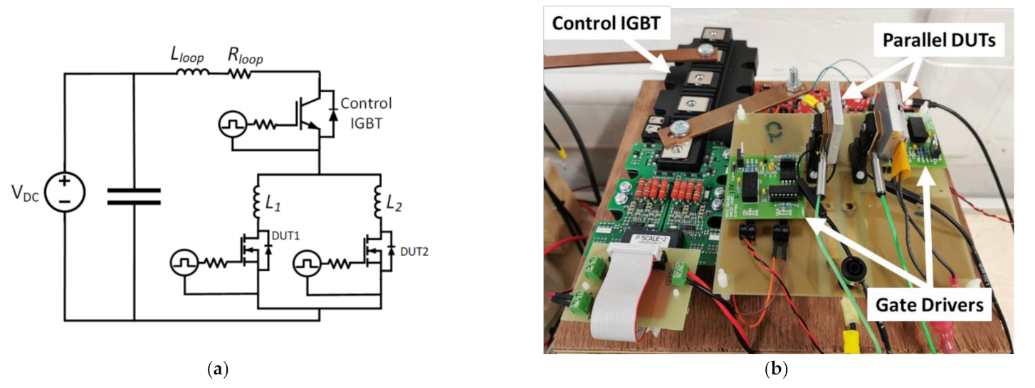
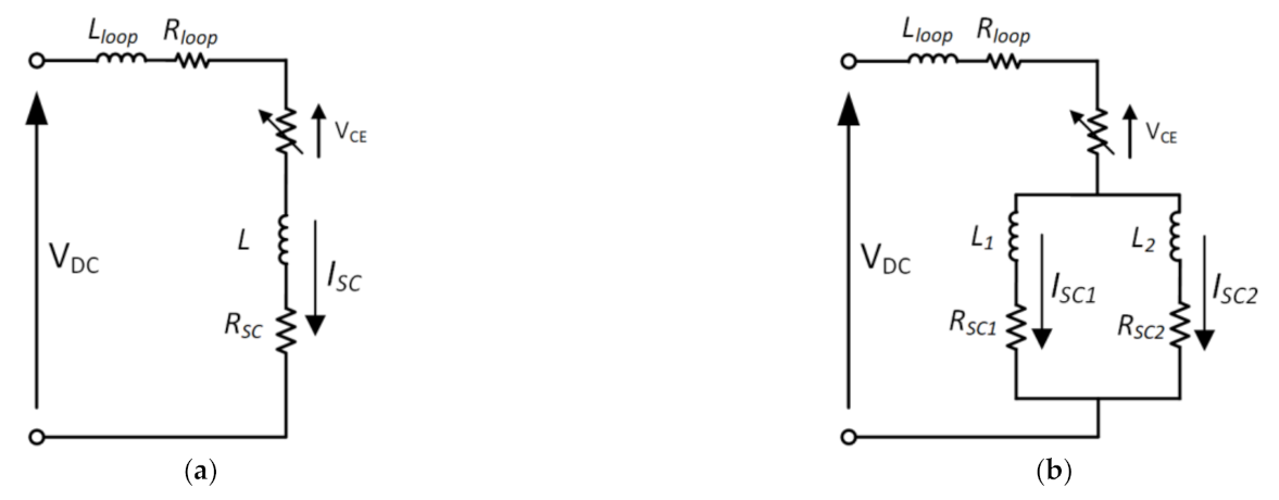
The experimental test rig circuit diagram is shown in Figure 1a, and the experimental circuit picture is shown in Figure 1b. In Figure 1a, Lloop is the total loop inductance, Rloop is the total loop resistance, L1 and L2 are the lumped total series parasitic inductance (internal device inductances plus PCB track inductance) of the parallel devices, and VDC is the supply voltage.
The test-rig comprises a DC power source, a 90 µF capacitor bank, a 1.2 kV/1 kA control IGBT module with datasheet reference FF1000R17IE4 and the devices under test (DUTs). Various of DUTs are tested including 1.2 kV planar MOSFETs, 1.2 kV SiC Trench MOSFETs, 650 V SiC Trench MOSFETs and 1.7 kV SiC Planar MOSFETs. Rogowski coils are used for current measurements and differential voltage probes are used for voltage measurements.
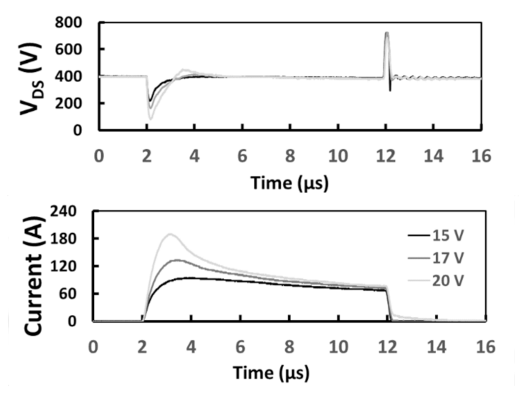
Figure 2 shows the measured voltage and current waveforms from the short circuit measurements for a single DUT (1.2 kV SiC planar MOSFET) driven with VGS = 15 V, 17 V and 20 V. The peak short circuit current increases with increased VGS due to reduced channel resistance. The negative and positive VDS spike at turn-ON and turn-OFF is due to the voltage drop across the parasitic inductance subtracting and adding to the device VDS voltage. The longer short circuit withstand times are due to the lower VDS of the measurements, which is a third of the device rating.
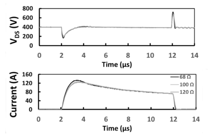
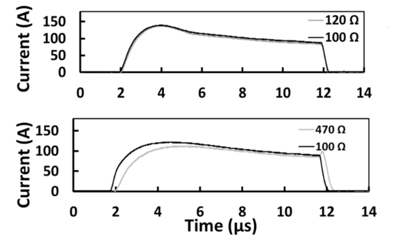
Figure 3 shows short circuit measurements for a 1.2 kV SiC Planar MOSFET with three different gate resistances, namely, RG = 68 Ω, 100 Ω and 120 Ω. The measurements show that the peak short circuit current increases marginally with reduced RG.
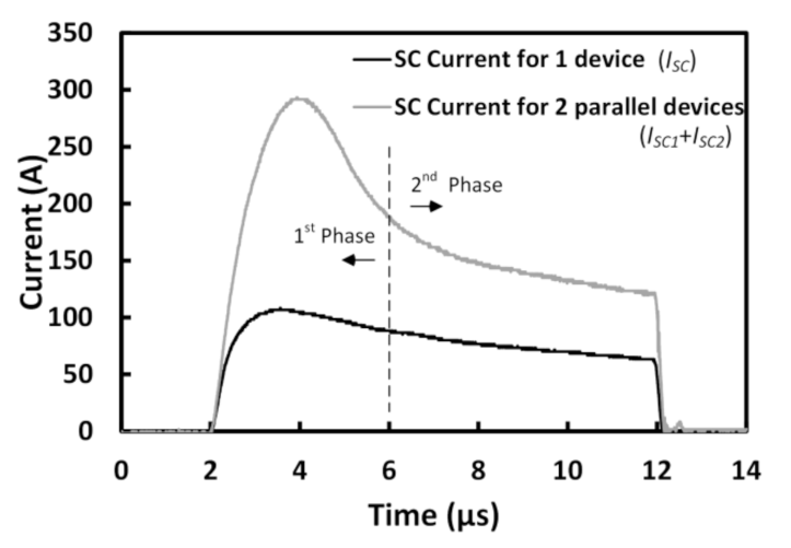
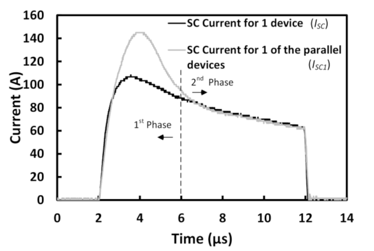
As devices are paralleled, it is expected that the total peak short circuit current increases due to the reduced SC resistance of the parallel pair. Figure 4 shows the measured SC currents for a single SiC MOSFET and a parallel pair. It can be observed that although the final SC current in the parallel devices is twice that of the single device, the peak SC current is approximately three times. This difference is due to the fact the SC currents have two phases. The first phase is limited by the series inductance and if affected by the threshold voltage, gate resistance and switching speed of the device. The second phase of the SC current is limited by the temperature coefficient of the short circuit resistance (RSC).
The trebling of the peak SC current is due to the paralleling of the device parasitic inductances. Hence, as devices are placed in parallel, the total SC current increases by more than a factor of the number of devices. Therefore, as the number of parallel devices is increased, the SC current per device increases, with the potential of leading to over-currents. This can be quantified considering the circuits in Figure 5a, which shows the equivalent circuit of the SC measurement of a single device (ISC), and Figure 5b, which shows the equivalent circuit for two parallel devices with SC currents ISC1 and ISC2. Figure 5a,b also shows the voltage drops in the series IGBT as well as the DC link parasitic inductance and resistance.
Figure 6 shows the comparison of ISC and ISC1. It can be seen from Figure 6 that during the first phase of the SC current, the peak SC current per device increases in the parallel devices compared to the single device (ISC1 is 37% greater ISC). However, in the second phase of the SC, the role of the parasitic inductance is minimized; hence, the SC current per device is independent of the number of parallel devices.
A key parameter in determining the impact of paralleling on the total SC current is the series parasitic inductance of the DC link. This DC link inductance will determine the difference between the peak currents ISC and ISC1 shown in Figure 6. The following model explains the role of this inductance.
From the equivalent circuit in Figure 5a, the SC current for a single device is given by Equation (1) below:
where VCE is the IGBT forward voltage, L is the lumped series parasitic inductance and RSC is the short circuit resistance of the single SiC MOSFET.
The parasitic inductance can be calculated by using the equation below. In the equation, is measured as overshoot voltage during the turn-OFF of the short-circuit as shown in Figure 2. This overshoot voltage is due to the total parasitic inductance, including the device drain inductance and parasitic inductance in series with the device.
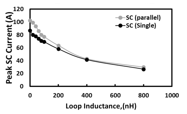
Assuming L1 = L2 = 50 nH (estimated parasitic source and drain inductances of a TO-247 package and PCB track), Rloop = 0.1 Ω, RSC1 = RSC2 = 3.5 Ω (derived as average resistance taken from measurements) and VDC = 400V, Equation (2) can be solved to show the impact of LDC on the SC current per device under parallel connection. Since the IGBT forward voltage (VCE) is significantly smaller than the supply voltage (VDC), this does not impact the SC currents. Figure 7 compares the calculated peak SC current for a single device and a device under parallel connection as a function of the busbar inductance. It can be seen from Figure 7 that the difference in the peak SC current between the single device and the single-device in parallel increases as the bus–bar inductance reduces. Hence, in applications that use power modules in circuits with low busbar inductance, the SC per device can be much higher than expected from a single device.
Measurements on parallel connected SiC MOSFETs with differences in VTH, RG and initial junction temperature have been performed. Differences in VTH can arise from variability in the manufacturing process and when that is minimized by careful pre-screening, VTH drift from BTI can cause VTH variation between parallel connected devices over the life of the power module. BTI is the process by which positive VGS stress causes VTH to increase due to negative charge trapping, and negative VGS stress causes VTH to decrease due to positive charge trapping. The higher interface and fixed oxide charges in SiC (due to the presence of carbon atoms during the gate oxidation process in the fabrication flow) is responsible for the more active nature of BTI in SiC MOSFETs. The random nature of trapped charge occurrence means that devices can exhibit varying degrees of VTH shift under identical conditions.
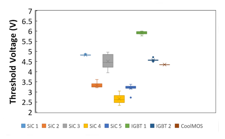
For SiC MOSFETs from different manufacturers, the threshold voltage distribution has been measured on a batch of devices. The threshold voltage was measured by shorting the drain to the gate, forcing 10 mA through the channel and measuring the VDS as described in [32]. Figure 8 shows the measured VTH distribution on devices from different manufacturers. The results show a wide range and standard deviation of VTH in SiC MOSFETs, hence emphasizing why it is important to analyze short circuit performance of parallel devices.
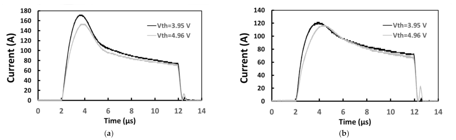
Figure 9a shows short circuit measurements on parallel connected 1.2 kV SiC Planar MOSFETs with 25% difference in VTH and VGS = 17 V, while Figure 9b shows similar measurements on the same device with VGS = 15 V. The measurements in Figure 9 show that a 25% difference in VTH leads to a 12.5% difference in the peak short circuit current at VGS = 17 V and 5% difference at VGS = 15 V. The device with the lower VTH has a higher peak SC current due to the reduced channel resistance according to Equation (3).
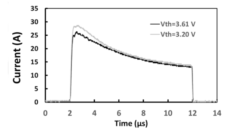
Similar measurements were performed on parallel connected 1.7 kV SiC MOSFET from another manufacturer and with a VTH difference of 12.8%. Figure 10 shows the short circuit measurement results, where the device with the lower VTH is shown to conduct 10% higher peak current. As the device voltage rating is increased, the short circuit current reduces due to higher ON-state resistance. The impact of VTH mismatch is apparent at both 1.2 and 1.7 kV voltage ratings. The main impact of the VTH mismatch is in the peak SC current. At the end of the SC pulse, the currents in both devices converge.
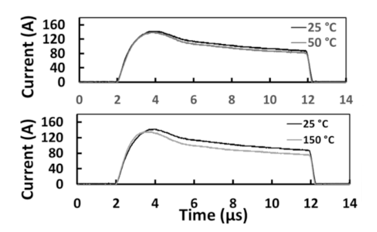
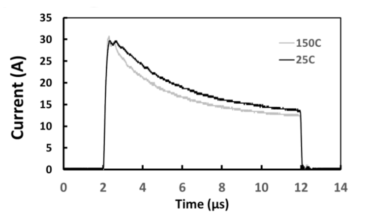
Measurements were performed on parallel devices set with different initial junction temperatures. Figure 11 shows the results of the SC measurements on the parallel connected 1.2 kV MOSFETs set with 100% and 500% difference in initial junction temperature. Initial junction temperature difference is important to consider because power devices on the same substrate can experience different rates of thermo-mechanical degradation. These differences in thermo-mechanical degradation rates can cause differences in the junction-to-case transient thermal impedance and hence differences in the junction temperature. The results in Figure 11 show that TJ mismatch in parallel connected devices has a marginal impact on the peak SC current unlike VTH mismatch where there is a more prominent difference in the peak SC current. Unlike the measurements in Figure 9 and Figure 10 corresponding with the VTH mismatch, the currents in Figure 11 do not converge over the SC duration. Figure 11 shows that a 100% difference in TJ leads to a 6.1% difference in the SC energy, while a 500% difference in Tj leads to a 12% difference in the SC energy with the higher TJ device dissipating less energy due to the higher temperature coefficient of the saturation resistance. Figure 12 shows similar measurements for parallel connected 1.7 kV SiC MOSFETs set with 500% difference in initial TJ.
The impact of differences in the MOSFET switching rate (controlled by RG) on current sharing under SC have also been analyzed. Over the operational life of the module, degradation in the gate wirebond can cause reduced switching rates in power devices due to increased gate current path impedance. Hence, it is possible that a power module undergoes a short circuit event with parallel devices that switch at different rates as a result of different degrees of gate wirebond degradation. Figure 13 shows the SC measurements on parallel connected 1.2 kV SiC MOSFETs with 20% and 370% difference in RG. A 20% difference in RG does not cause any difference in the SC characteristics, whereas a 370% difference in RG causes a 5.7% difference in the SC energy with the faster switching device dissipating more SC Energy. Because a 370% difference in RG is high and is indicative of significant reliability problems, it can be concluded that small and moderate differences in RG do not impact the performance of the module under SC conditions.
3. BTI and SC Measurements
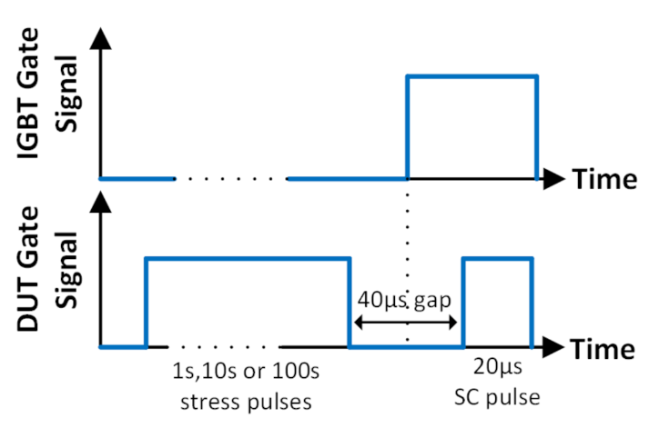
In this section, the impact of threshold voltage shift (ΔVTH) from BTI on short circuit characteristics of SiC MOSFETs were investigated. In SiC MOSFETs, biasing the gate terminal is known to cause a threshold voltage shift [33], which depends on the magnitude and duration of the bias stress. This ΔVTH can have implications on the SC performance of SiC MOSFETs, and this has been experimentally characterized in this section. The experiment is performed by applying a pre-stress VGS pulse on the gate of the SiC device before testing the DUT under short circuit conditions. The pulse sequence is shown in Figure 14, where the control IGBT gate pulse and the DUT pulse is shown.
The short-circuit tests (duration of 20 µs at a DC link voltage of 200 V) is performed 40 µs after stress removal, thereby minimizing the impact of the recovery time on the measured SC current. A time of 40 µs was chosen to allow sufficient time for the IGBT to turn-ON while also capturing the influence of trapped charges on the short circuit performance since VTH recovery from the release of trapped charges can affect the measurements. This recovery after stress removal in one of the main challenges of BTI characterization in SiC MOSFETs [20,21,22]. The duration of the pre-test VGS stress pulse is varied as to investigate the impact of pulse duration on the SC characteristics. The selected value of VGS for stress and the SC evaluation is 17 V.
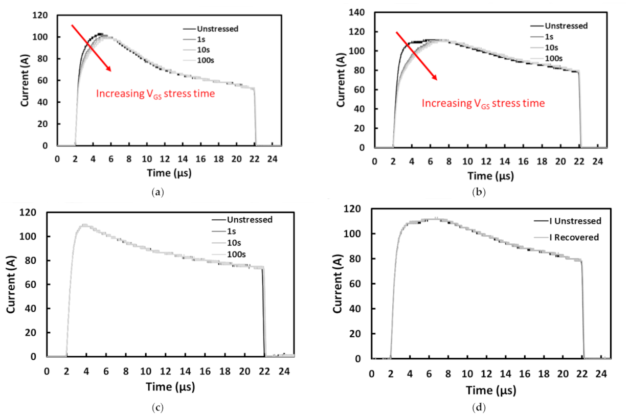
The results of the test described in Figure 14 are shown in Figure 15a for the 1.2 kV SiC Trench MOSFET, Figure 15b for the 1.2 kV SiC Planar MOSFET and Figure 15c for a silicon IGBT device. All the measurements in Figure 15 have been performed at a case temperature of 25 °C. The results for the SiC MOSFETs in Figure 15a,b show a slightly reduced short circuit charge as the VGS stress duration increases from 1 s to 100 s. The application of the pre-test VGS voltage causes a rise in VTH due to negative charge trapping [34], which subsequently causes a reduction in the short circuit current. Similar measurements performed on a 650 V silicon IGBT are shown in Figure 15c. It is apparent that the SC characteristics of the IGBT remain invariant of pre-test VGS stress pulses. The results in Figure 15 indicate that while BTI impacts the SC characteristics of SiC devices, it has no impact on silicon IGBTs.
After sufficient recovery time, the VTH of the stressed device reverts back to its pre-stressed value since all the trapped negative charges are subsequently released. Figure 15d shows the SC measurements of the fully recovered device where the recovery time was 15 min. It can be seen from Figure 15d that the SC characteristics are identical to that measured in the unstressed device; hence, the VTH has recovered fully to the pre-stress value.
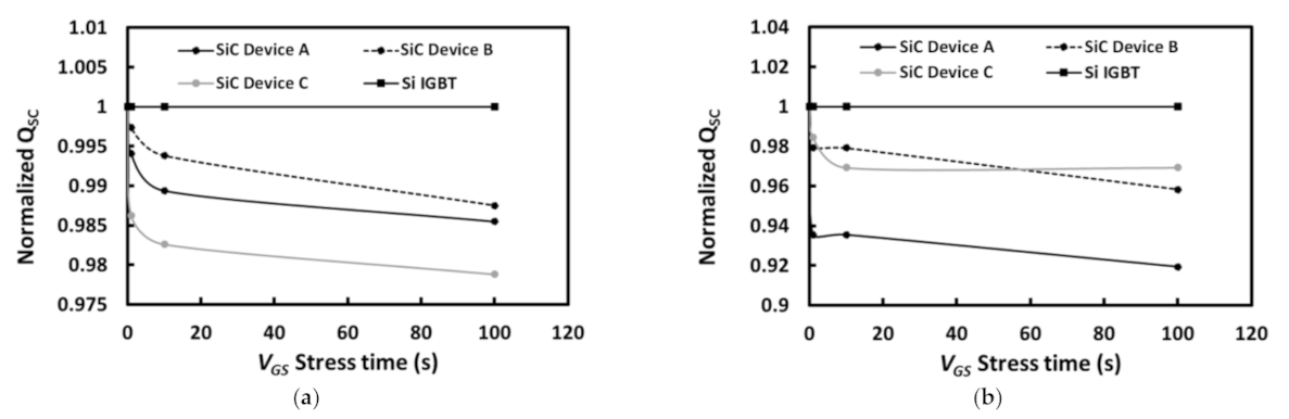
The short circuit current was integrated over time to yield the SC charge. Figure 16a shows the normalized short circuit charge for 3 SiC MOSFETs and 1 silicon IGBT after undergoing a combination of BTI and SC tests. The reduction in the SC charge after BTI stress is apparent for the SiC MOSFETs but not in the silicon IGBT. The reduction in SC charge ranges between 5% and 25% for the SiC MOSFETs. At face value, a reduction in SC charge/current due to an increase in VTH (from negative charge trapping) may not be negative consequences since the SC energy is reduced for the device; however, this can have a significant impact on the reliability of parallel connected SiC MOSFETs under SC conditions. Non-uniform current sharing of SiC MOSFETs under SC conditions has been cited as the primary cause of power module failure under SCs [16].
The combined BTI and SC measurements were repeated at a case temperature of 150 °C for different stress times to investigate the impact of temperature on BTI and SC current. The results are shown in Figure 16b. Comparing the SC measurements (after BTI stress) in Figure 16a,b shows that temperature increases the extent of VTH increase leading to SC charge reduction. All devices exhibit increased effect of VTH shift as temperature is increased; however, the change is not uniform. Device A shows a SC charge that reduces by 1.5% for VGS stress at 25 °C to 8% at 150 °C. Device B shows a SC charge that reduces by 1% for VGS stress at 25 °C to 4% at 150 °C. Device C shows a SC charge that reduces by 2% for VGS stress at 25 °C to 3% at 150 °C. These measurements were also performed on the Si IGBT, and as can be seen from the Figure 16, there has been no change in the SC charge due to VGE stress or temperature.
4. Datasheet-Based Thermal Modeling and Finite Element Electrothermal Simulations of Short Circuits
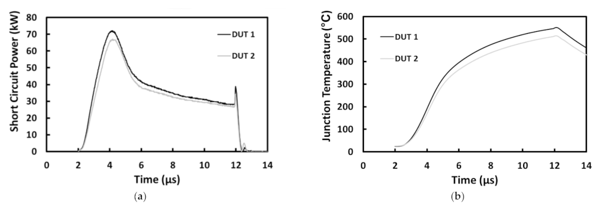
Simulations have been performed to investigate the impact of VTH mismatch on the junction temperatures of the power devices. The goal of the datasheet-based thermal modeling here is to use experimental SC measurements combined with a datasheet-provided thermal network to estimate the device junction temperature. First, the measured short circuit power from the experimental results is fed into the 5-layer Cauer thermal network provided by the manufacturer, and the resulting junction temperatures are evaluated. The devices are mounted in different heatsinks (as shown in Figure 1b); hence, the mutual thermal impedance can be neglected. Figure 17a shows the measured short circuit power for the parallel DUTs, while Figure 17b shows the simulated junction temperatures. Since experimental measurements (shown in Figure 17a) are used for evaluating junction temperature, the temperature dependencies of the device parameters and therefore self-heating, are already considered. Additionally, the transient thermal impedance characteristics provided on the datasheet is experimentally derived, the temperature dependencies of the thermal resistance and capacitances are accounted for. Figure 17b shows that there is a 6.8% difference in the peak junction temperatures between the two devices. Since the thermal simulations assume uniform temperature distribution in the power device, the temperatures in Figure 17b are likely underestimated values of the temperature hot-spots within the chip.
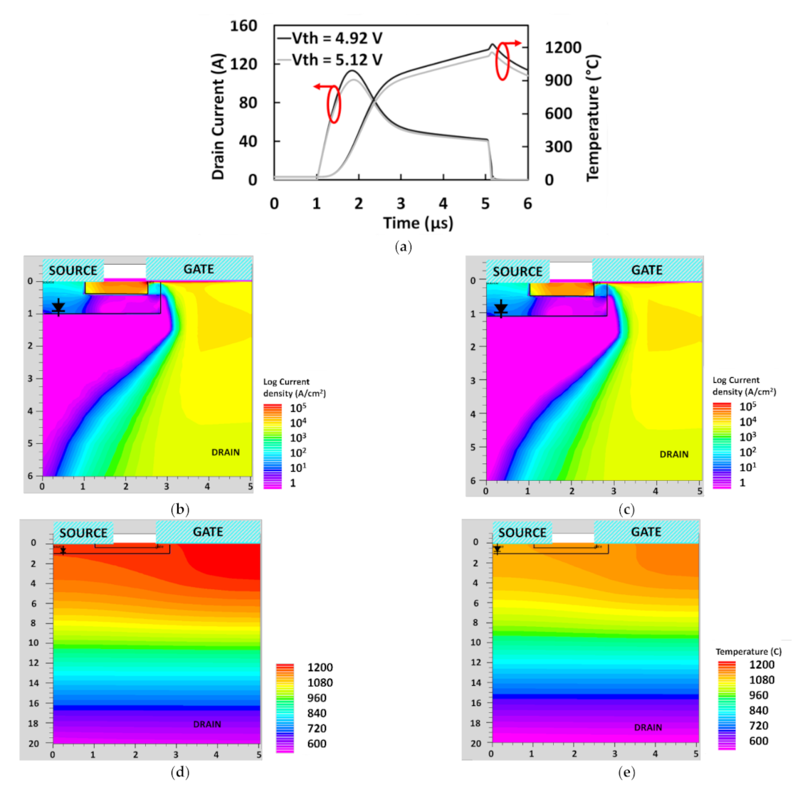
To investigate the impact of VTH shift on the internal current and temperature distribution of SiC MOSFETs, finite element simulations of SiC MOSFETs under short-circuit conditions have been performed in ATLAS (from Silvaco). For this investigation, a 2D model for a SiC MOSFET cell was simulated with the drift layer thickness and doping designed to achieve the required breakdown voltage. The thermal boundary conditions were defined in the simulation by specifying a lumped thermal resistance and capacitance chosen to replicate the thermal characteristics of the device according to the datasheet. The simulation solves the drift–diffusion equations fully coupled with the heat flow equation to yield a thermal map identifying the hot-spot location within the MOSFET cell. The temperature dependency of all semiconductor parameters (effective mobility and intrinsic carrier concentration) is accounted for. This 2D model can provide a qualitative insight of the temperature and current distributions within the device. Table 1 shows the parameters used in the finite element model. The threshold voltage of the MOSFET in the simulation is controlled by varying the doping in the current spreading layer. By varying this doping between parallel devices, the electrothermal dynamics of current sharing can be investigated using the simulator.
Figure 18a shows the simulated SC current and hot-spot temperature of 2 parallel SiC MOSFETs with 4% difference in VTH. The hot-spot temperature (shown in Figure 18a) within the device is approximately double that predicted by the compact model in Figure 17b, which uses the manufacturer provided thermal network. Figure 18b,c compares the current density for the simulated parallel devices with 4% difference in VTH, while Figure 16e and Figure 18d compare the hot-spot temperatures. Higher current density and lattice temperature can be observed in the device with the lower VTH with a corresponding larger hot-spot area compared to the device with the higher VTH.
5. Conclusions
This paper investigated the impact of variations in the threshold voltage, initial junction temperature and gate resistance on the sharing of SC current in parallel power devices. The results show that variations in VTH are most critical to SC current sharing. The SC current per device increases with the number of parallel devices due to the reduction of the total inductance across the voltage source. Hence, current sharing in large current capacity power modules is more critical as the number of parallel devices increases. VTH shift from BTI in SiC MOSFETs is well understood to be a more challenging reliability concern compared to silicon devices. This paper shows that VGS stresses on the gate oxide of SiC MOSFETs at the rated VGS is capable of causing a change in the peak SC current and SC charge due to VTH shift. Subsequent measurements of SC currents 15 min after the stress have shown a reversion to the pre-stress SC characteristics, thereby indicating a release of the trapped charge and a restoration of the pre-stress VTH. The change in the peak SC current and SC charge is proportional to the VGS stress duration and temperature, thereby indicating that the time constants of the trapped charge have a negative temperature coefficient. Electrothermal simulations have shown that a 25% difference in VTH between parallel connected SiC MOSFETs under SC can result in 6.8% difference in the peak junction temperature. Finite element simulations of SiC MOSFETs under short-circuit conditions show that the hot-spot temperatures are at least twice those predicted from manufacturer provided thermal models. The issue of VTH mismatch and BTI is shown to be assessed in SiC MOSFETs, and an experimental methodology has been presented to quantify the effects.
Author Contributions
Conceptualization, O.A. and J.O.G.; methodology, O.A., J.O.G. and R.W.; software, R.W., N.A. and S.M.; validation, R.W. and J.O.G.; formal analysis, R.W., O.A., S.M., J.O.G. and N.A.; investigation, R.W., S.M., N.A. and S.J.; resources, O.A.; data curation, R.W. and O.A.; writing—original draft preparation, O.A.; writing—review and editing, J.O.G., R.W. and S.J.; visualization, O.A., R.W. and N.A.; supervision, O.A.; project administration, O.A.; funding acquisition, O.A. All authors have read and agreed to the published version of the manuscript.
Funding
This work was funded by the UK Engineering and Physical Science Research Council (EPSRC) through the grant reference EP/R004366/1.
Institutional Review Board Statement
Not applicable.
Informed Consent Statement
Not applicable.
Data Availability Statement
Not applicable.
Conflicts of Interest
The authors declare no conflict of interest. The funders had no role in the design of the study; in the collection, analyses, or interpretation of data; in the writing of the manuscript; or in the decision to publish the results.
References
- Sun, J.; Xu, H.; Wu, X.; Yang, S.; Guo, Q.; Sheng, K. Short circuit capability and high temperature channel mobility of SiC MOSFETs. In Proceedings of the 2017 29th International Symposium on Power Semiconductor Devices and IC’s (ISPSD), Sapporo, Japan, 28 May–1 June 2017; pp. 399–402. [Google Scholar]
- Romano, G.; Fayyaz, A.; Riccio, M.; Maresca, L.; Breglio, G.; Castellazzi, A.; Irace, A. A Comprehensive study of short-circuit ruggedness of silicon carbide power MOSFETs. IEEE J. Emerg. Sel. Top. Power Electron. 2016, 4, 978–987. [Google Scholar] [CrossRef]
- Castellazzi, A.; Fayyaz, A.; Romano, G.; Yang, L.; Riccio, M.; Irace, A. SiC power MOSFETs performance, robustness and technology maturity. Microelectron. Reliab. 2016, 58, 164–176. [Google Scholar] [CrossRef]
- Qin, H.; Dong, Y.; Xu, K.; Xu, H.; Fu, D.; Wang, S.; Zhao, C. A comprehensive study of the short-circuit characteristics of SiC MOSFETs. In Proceedings of the 2017 12th IEEE Conference on Industrial Electronics and Applications (ICIEA), Siem Reap, Cambodia, 18–20 June 2017; pp. 332–336. [Google Scholar]
- Xing, D.; Hu, B.; Yu, S.; Zhang, Y.; Liu, T.; Salemi, A.; Kang, M.; Wang, J.; Agarwal, A. Current saturation characteristics and single-pulse short-circuit tests of commercial SiC MOSFETs. In Proceedings of the 2019 IEEE Energy Conversion Congress and Exposition (ECCE), Baltimoe, MD, USA, 29 September–3 October 2019; pp. 6179–6183. [Google Scholar]
- Romano, G.; Maresca, L.; Riccio, M.; D’Alessandro, V.; Breglio, G.; Irace, A.; Fayyaz, A.; Castellazzi, A. Short-circuit failure mechanism of SiC power MOSFETs. In Proceedings of the 2015 IEEE 27th International Symposium on Power Semiconductor Devices & IC’s (ISPSD), Hong Kong, China, 10–14 May 2015; pp. 345–348. [Google Scholar]
- Okawa, M.; Aiba, R.; Kanamori, T.; Yano, H.; Iwamuro, N.; Harada, S. Experimental and numerical investigations of short-circuit failure mechanisms for state-of-the-art 1.2 kV SiC trench MOSFETs. In Proceedings of the 2019 31st International Symposium on Power Semiconductor Devices and ICs (ISPSD), Shanghai, China, 19–23 May 2019; pp. 167–170. [Google Scholar]
- Chen, X.; Chen, H.; Shi, B.; Wang, Y.; Li, X.; Zhou, C.; Li, C.; Deng, X.; Luo, H.; Wu, Y.; et al. Investigation on short-circuit characterization and optimization of 3.3-kV SiC MOSFETs. IEEE Trans. Electron. Devices 2021, 68, 184–191. [Google Scholar] [CrossRef]
- Agarwal, A.; Kanale, A.; Han, K.; Baliga, B.J.; Bhattacharya, S. Impact of gate oxide thickness on switching and short circuit performance of 1200 V 4H-SiC inversion-channel MOSFETs. In Proceedings of the 2019 IEEE 7th Workshop on Wide Bandgap Power Devices and Applications (WiPDA), Raleigh, NC, USA, 29–31 October 2019; pp. 59–62. [Google Scholar]
- Tani, K.; Sakano, J.I.; Shima, A. Analysis of short-circuit break-down point in 3.3 kV SiC-MOSFETs. In Proceedings of the 2018 IEEE 30th International Symposium on Power Semiconductor Devices and ICs (ISPSD), Chicago, IL, USA, 14–17 May 2018; pp. 383–386. [Google Scholar]
- Agarwal, A.; Kanale, A.; Han, K.; Baliga, B.J. Switching and short-circuit performance of 27 nm gate oxide, 650 V SiC planar-gate MOSFETs with 10 to 15 V gate drive voltage. In Proceedings of the 2020 32nd International Symposium on Power Semiconductor Devices and ICs (ISPSD), Vienna, Austria, 13–18 September 2020; pp. 250–253. [Google Scholar]
- Sun, J.; Wei, J.; Zheng, Z.; Wang, Y.; Chen, K.J. Short circuit capability and short circuit induced VTH instability of a 1.2-kV SiC power MOSFET. IEEE J. Emerg. Sel. Top. Power Electron. 2019, 7, 1539–1546. [Google Scholar] [CrossRef]
- Zou, Q.; Ke, J.; Peng, J.; Zhao, Z. Effect of parasitic inductance mismatch on short-circuit characterization of paralleled SiC MOSFETs. In Proceedings of the 2019 4th IEEE Workshop on the Electronic Grid (eGRID), Xiamen, China, 11–14 November 2019; IEEE: New York, NY, USA, 2019; pp. 1–8. [Google Scholar]
- Ionita, C.; Nawaz, M.; Ilves, K.; Iannuzzo, F. Short-circuit ruggedness assessment of a 1.2 kV/180 A SiC MOSFET power module. In 2017 IEEE Energy Conversion Congress and Exposition (ECCE); IEEE: New York, NY, USA, 2017; pp. 1982–1987. [Google Scholar]
- An, J.; Namai, M.; Yano, H.; Iwamuro, N.; Kobayashi, Y.; Harada, S. Methodology for enhanced short-circuit capability of SiC MOSFETs. In Proceedings of the 2018 IEEE 30th International Symposium on Power Semiconductor Devices and ICs (ISPSD), Chicago, IL, USA, 13–17 May 2018; pp. 391–394. [Google Scholar]
- Richardeau, F.; Boige, F.; Castellazzi, A.; Chazal, V.; Fayyaz, A.; Borghese, A.; Irace, A.; Guibaud, G. SiC MOSFETs soft and hard failure modes: Functional analysis and structural characterization. In Proceedings of the 2020 32nd International Symposium on Power Semiconductor Devices and ICs (ISPSD), Vienna, Austria, 13–18 September 2020; pp. 170–173. [Google Scholar]
- Unger, C.; Pfost, M. Investigation of gate and drain leakage currents during the short circuit of SiC-MOSFETs. In Proceedings of the 2020 32nd International Symposium on Power Semiconductor Devices and ICs (ISPSD), Vienna, Austria, 13–18 September 2020; pp. 238–241. [Google Scholar]
- Wei, J.; Liu, S.; Yang, L.; Fang, J.; Li, T.; Li, S.; Sun, W. Comprehensive analysis of electrical parameters degradations for SiC power MOSFETs under repetitive short-circuit stress. IEEE Trans. Electron. Devices 2018, 65, 5440–5447. [Google Scholar] [CrossRef]
- Du, H.; Reigosa, P.D.; Iannuzzo, F.; Ceccarelli, L. Impact of the case temperature on the reliability of SiC MOSFETs under repetitive short circuit tests. In Proceedings of the 2019 IEEE Applied Power Electronics Conference and Exposition (APEC), Anaheim, CA, USA, 17–21 March 2019; pp. 332–337. [Google Scholar]
- Zhou, X.; Su, H.; Wang, Y.; Yue, R.; Dai, G.; Li, J. Investigations on the degradation of 1.2-kV 4H-SiC MOSFETs under repetitive short-circuit tests. IEEE Trans. Electron. Devices 2016, 63, 4346–4351. [Google Scholar] [CrossRef]
- Xing, D.; Lyu, X.; Liu, J.; Xie, C.; Agarwal, A.; Wang, J. 3300-V SiC MOSFET short-circuit reliability and protection. In Proceedings of the 2021 IEEE Applied Power Electronics Conference and Exposition (APEC), Online Conference, 14–17 June 2021; pp. 1262–1266. [Google Scholar]
- Xing, D.; Xie, C.; Wang, K.; Liu, T.; Hu, B.; Wang, J.; Agarwal, A.; Singh, R.; Atcitty, S. 3.3-kV SiC MOSFET performance and short-circuit capability. In Proceedings of the 2020 IEEE Workshop on Wide Bandgap Power Devices and Applications in Asia (WiPDA Asia), Online Conference, 23–25 September 2020; pp. 1–6.
- Ji, S.; Laitinen, M.; Huang, X.; Sun, J.; Giewont, B.; Tolbert, L.M.; Wang, F. Short circuit characterization of 3rd generation 10 kV SiC MOSFET. In Proceedings of the 2018 IEEE Applied Power Electronics Conference and Exposition (APEC), San Antonio, TX, USA, 4–8 March 2018; pp. 2775–2779. [Google Scholar]
- Ji, S.; Laitinen, M.; Huang, X.; Sun, J.; Giewont, W.; Wang, F.; Tolbert, L.M. Short-circuit characterization and protection of 10-kV SiC mosfet. IEEE Trans. Power Electron. 2019, 34, 1755–1764. [Google Scholar] [CrossRef]
- Reigosa, P.D.; Iannuzzo, F.; Luo, H.; Blaabjerg, F. A short-circuit safe operation area identification criterion for SiC MOSFET power modules. IEEE Trans. Ind. Appl. 2017, 53, 2880–2887. [Google Scholar] [CrossRef] [Green Version]
- Kadavelugu, A.; Aeloiza, E.; Belcastro, C. Short-circuit performance of multi-chip SiC MOSFET modules. In Proceedings of the 2017 IEEE 5th Workshop on Wide Bandgap Power Devices and Applications (WiPDA), Albuquerque, NM, USA, 30 October–1 November 2017; pp. 285–290. [Google Scholar] [CrossRef]
- Ke, J.; Zhao, Z.; Zou, Q.; Peng, J.; Chen, Z.; Cui, X. Device screening strategy for balancing short-circuit behavior of paralleling silicon carbide MOSFETs. IEEE Trans. Device Mater. Reliab. 2019, 19, 757–765. [Google Scholar] [CrossRef]
- Boige, F.; Fayyaz, A.; Castellazzi, A.; Richardeau, F.; Vinnac, S. Short-circuit robustness of parallel SiC MOSFETs and fail-safe mode strategy. In Proceedings of the 2019 21st European Conference on Power Electronics and Applications (EPE ’19 ECCE Europe), Genova, Italy, 2–5 September 2019. [Google Scholar]
- Peters, D.; Aichinger, T.; Basler, T.; Rescher, G.; Puschkarsky, K.; Reisinger, H. Investigation of threshold voltage stability of SiC MOSFETs. In Proceedings of the 2018 IEEE 30th International Symposium on Power Semiconductor Devices and ICs (ISPSD), Chicago, IL, USA, 13–17 May 2018; pp. 40–43. [Google Scholar]
- Gonzalez, J.A.O.; Alatise, O. Impact of BTI-induced threshold voltage shifts in shoot-through currents from crosstalk in SiC MOSFETs. IEEE Trans. Power Electron. 2021, 36, 3279–3291. [Google Scholar] [CrossRef]
- Gonzalez, J.A.O.; Alatise, O. A novel non-intrusive technique for BTI characterization in SiC mosfets. IEEE Trans. Power Electron. 2019, 34, 5737–5747. [Google Scholar] [CrossRef] [Green Version]
- Habersat, D.B.; Lelis, A.J.; Green, R. Measurement considerations for evaluating BTI effects in SiC MOSFETs. Microelectron. Reliab. 2018, 81, 121–126. [Google Scholar] [CrossRef]
- Aichinger, T.; Rescher, G.; Pobegen, G. Threshold voltage peculiarities and bias temperature instabilities of SiC MOSFETs. Microelectron. Reliab. 2018, 80, 68–78. [Google Scholar] [CrossRef]
- Gonzalez, J.O.; Alatise, O. Bias temperature instability and junction temperature measurement using electrical parameters in SiC power MOSFETs. IEEE Trans. Ind. Appl. 2021, 57, 1664–1676. [Google Scholar] [CrossRef]
Figure 1.
Experiment setup: (a) experimental test-rig circuit diagram for short circuit measurements; (b) experimental test-rig picture.
Figure 1.
Experiment setup: (a) experimental test-rig circuit diagram for short circuit measurements; (b) experimental test-rig picture.

Figure 2.
Short circuit measurements for VDS and current in SiC MOSFET with VGS = 15 V, 17 V and 20 V.
Figure 2.
Short circuit measurements for VDS and current in SiC MOSFET with VGS = 15 V, 17 V and 20 V.

Figure 3.
Short circuit measurements for VDS and current in SiC MOSFET with RG = 68, 100 and 120 Ω.

Figure 4.
Measurements of SC current for a single SiC MOSFET and 2 parallel SiC MOSFETs.

Figure 5.
Equivalent circuit of devices under test: (a) single device under short circuit; (b) parallel-connected devices under short circuit.
Figure 5.
Equivalent circuit of devices under test: (a) single device under short circuit; (b) parallel-connected devices under short circuit.

Figure 6.
Measurement of the short circuit currents through a 650 V SiC Trench MOSFET under single device short circuit condition and under parallel short circuit condition.
Figure 6.
Measurement of the short circuit currents through a 650 V SiC Trench MOSFET under single device short circuit condition and under parallel short circuit condition.

Figure 7.
Calculated peak SC current for single and parallel MOSFET as a function of total loop inductance.
Figure 7.
Calculated peak SC current for single and parallel MOSFET as a function of total loop inductance.

Figure 8.
VTH distribution on devices from different manufacturers.

Figure 9.
Measured short circuit current for parallel 1.2 kV/20 A SiC MOSFETs with 25% difference in VTH: (a) VGS = 17 V; (b) VGS = 15 V.
Figure 9.
Measured short circuit current for parallel 1.2 kV/20 A SiC MOSFETs with 25% difference in VTH: (a) VGS = 17 V; (b) VGS = 15 V.

Figure 10.
Measured short circuit current for parallel 1.7 kV/5 A SiC MOSFETs with 12.8% difference in VTH.
Figure 10.
Measured short circuit current for parallel 1.7 kV/5 A SiC MOSFETs with 12.8% difference in VTH.

Figure 11.
Measured short circuit current for parallel 1.2 kV/20 A SiC MOSFETs with 100% and 500% difference in Tj.
Figure 11.
Measured short circuit current for parallel 1.2 kV/20 A SiC MOSFETs with 100% and 500% difference in Tj.

Figure 12.
Measured short circuit current for parallel 1.7 kV/5 A SiC MOSFETs with different junction temperatures.
Figure 12.
Measured short circuit current for parallel 1.7 kV/5 A SiC MOSFETs with different junction temperatures.

Figure 13.
Measured short circuit current for parallel 1.2 kV/20 A SiC MOSFETs with 20% and 370% difference in RG.
Figure 13.
Measured short circuit current for parallel 1.2 kV/20 A SiC MOSFETs with 20% and 370% difference in RG.

Figure 14.
Gate pulse signals for the IGBT and DUT for BTI and SC tests.

Figure 15.
Impact of BTI on SC currents for devices: (a) 1.2 kV SiC Trench MOSFET; (b) 1.2 kV SiC Planar MOSFET; (c) 650 V Silicon IGBT; (d) SC measurements performed on fully recovered SiC Planar MOSFET showing VTH is restored to its pre-test value.
Figure 15.
Impact of BTI on SC currents for devices: (a) 1.2 kV SiC Trench MOSFET; (b) 1.2 kV SiC Planar MOSFET; (c) 650 V Silicon IGBT; (d) SC measurements performed on fully recovered SiC Planar MOSFET showing VTH is restored to its pre-test value.

Figure 16.
Impact of BTI on SC charge for 1.2 kV SiC MOSFETs and Si IGBT at a case temperature of (a) 25 °C, and (b) 150 °C. Impact of VGS stress time is apparent for SiC MOSFETs.
Figure 16.
Impact of BTI on SC charge for 1.2 kV SiC MOSFETs and Si IGBT at a case temperature of (a) 25 °C, and (b) 150 °C. Impact of VGS stress time is apparent for SiC MOSFETs.

Figure 17.
Measured SC power and simulated temperature for the parallel 1.2 kV SiC MOSFETs with 25% difference in VTH: (a) measured SC power; (b) simulated temperature.
Figure 17.
Measured SC power and simulated temperature for the parallel 1.2 kV SiC MOSFETs with 25% difference in VTH: (a) measured SC power; (b) simulated temperature.

Figure 18.
Simulated SC current and hot-spot temperature using finite elemental model and 2D plot results taken at 4 us into the short circuit for the SiC MOSFET: (a) simulated SC current and hot-spot temperature; (b) 2D current density plot (VTH = 4.92 V); (c) 2D current density plot (VTH = 5.12 V); (d) 2D temperature contour plot of the SiC MOSFET (VTH = 4.92 V); (e) 2D temperature contour plot of the SiC MOSFET (VTH = 5.12 V).


Table 1.
Simulation parameters.
| Parameter | MOSFET 1 | MOSFET 2 |
|---|---|---|
| Source doping (cm−3) | 1 × 10¹⁹ | 1 × 10¹⁹ |
| Channel length (µm) | 0.2 | 0.2 |
| Drift thickness (µm) | 8 | 8 |
| Drift doping (cm−3) | 1.5 × 10¹⁵ | 1.5 × 10¹⁵ |
| Channel doping (cm−3) | 1.5 × 10¹⁷ | 1.5 × 10¹⁷ |
| Drain doping (cm−3) | 1 × 10¹⁹ | 1 × 10¹⁹ |
| Oxide thickness (nm) | 50 | 50 |
| Thermal resistance (K/W) | 0.39 | 0.39 |
| Current spreading layer doping (cm−3) | 1.5 × 10¹⁶ | 1 × 10¹⁶ |
Publisher’s Note: MDPI stays neutral with regard to jurisdictional claims in published maps and institutional affiliations. |
© 2021 by the authors. Licensee MDPI, Basel, Switzerland. This article is an open access article distributed under the terms and conditions of the Creative Commons Attribution (CC BY) license (https://creativecommons.org/licenses/by/4.0/).
Share and Cite
MDPI and ACS Style
Wu, R.; Mendy, S.; Agbo, N.; Gonzalez, J.O.; Jahdi, S.; Alatise, O. Performance of Parallel Connected SiC MOSFETs under Short Circuits Conditions. Energies 2021, 14, 6834. https://doi.org/10.3390/en14206834
AMA Style
Wu R, Mendy S, Agbo N, Gonzalez JO, Jahdi S, Alatise O. Performance of Parallel Connected SiC MOSFETs under Short Circuits Conditions. Energies. 2021; 14(20):6834. https://doi.org/10.3390/en14206834
Chicago/Turabian StyleWu, Ruizhu, Simon Mendy, Nereus Agbo, Jose Ortiz Gonzalez, Saeed Jahdi, and Olayiwola Alatise. 2021. "Performance of Parallel Connected SiC MOSFETs under Short Circuits Conditions" Energies 14, no. 20: 6834. https://doi.org/10.3390/en14206834
Note that from the first issue of 2016, this journal uses article numbers instead of page numbers. See further details here.