Analysis and Verification of a Wide Input Voltage PWM Converter with Variable Windings

Department of Electrical Engineering, National Yunlin University of Science and Technology, Yunlin 640, Taiwan
*
Author to whom correspondence should be addressed.
Energies 2020, 13(7), 1634; https://doi.org/10.3390/en13071634
Submission received: 4 March 2020
/
Revised: 28 March 2020
/
Accepted: 30 March 2020
/
Published: 2 April 2020
(This article belongs to the Special Issue Design and Analysis of Electric Machines)
Abstract
:A three-leg pulse-width modulation converter with auxiliary windings is provided and investigated to realize wide voltage operation and zero voltage switching characteristics on power switches. The presented converter has three converter legs on the input-side and two sets of winding turns on the output-side. Owing to the on/off states of the three converter legs and the two sets of secondary winding turns, the proposed converter can be operated under three different equivalent circuits to have wide input voltage operation from 30V ~ 240V (Vin,max = 8Vin,min). Compared with the multi-stage converters to realize wide input voltage operation, the proposed circuit topology has fewer circuit components and a simple control algorithm. Conventional duty cycle control with phase-shift between each converter leg is adopted to regulate load voltage and also accomplish zero voltage switching on active switches. The presented three-leg converter is tested with a laboratory circuit. Finally, experiments testify to the performance and validity of the presented converter.
1. Introduction
Renewable energy sources are widely developed and investigated to lessen fossil fuel demand and reduce air pollution. From many renewable power sources, solar or wind power is more attractive due to the cost effectiveness. Power electronics play a more and more important role to convert the unstable input voltage from solar panels and wind generators to a stable direct-current (DC) or alternative-current (AC) voltage. Power electronics have been developed for low power (such as personal computer power units, battery chargers, consumer electronics, and solid-state lighting systems) and medium power applications (such as server power units, DC micro grid power conversion, and renewable energy power conversion). Due to the wide deviation of wind speed or solar intensity, the output voltage of wind generators or photovoltaic panels is not constant. The maximum output voltage versus minimum output voltage of the solar panels may be greater than 4:1. Conventional DC converters with wide voltage operation [1,2,3,4,5,6,7] for wind and solar power conversion are based on the circuit topologies of series-parallel connection or multi-stage conversion. However, the multi-stage circuit structure will result in low circuit efficiency and reliability. The wide voltage DC converters were studied in [8,9,10,11,12] to have soft switching operation and high efficiency. However, the complicated control scheme is the main drawback for these circuit topologies. The series and parallel resonant converters have been developed for lighting and industry applications [13,14]. The switching frequency of the resonant converters are dependent on the load conditions. The power switches turn on under zero voltage. Therefore, the switching losses are improved under high frequency operation. Compared with series or parallel resonant converters, the LLC (inductor-inductor-capacitor) resonant converters [15,16,17,18] are more attractive in consumer and industry applications such as server power and power units in personal computers and plug-in hybrid electric vehicles. Unfortunately, the narrow voltage range and wide switching frequency range are the main drawbacks of the LLC converters. For photovoltaic and fuel cell power applications, the solar panel or fuel cell output is a variable voltage that is related to the solar intensity. The low power units of railway systems, the input voltage of DC converters for motor drive controllers, lighting systems, electric door systems, and braking systems may be variated from 24 V to 110 V. For hybrid electric vehicle or electric vehicle systems, the output voltage of battery chargers is varied between 200 V and 450 V. Therefore, the wide voltage DC converters [19,20,21] have been developed as the interface circuits to convert the solar power to electric power. In [21], the PWM converter was presented with two transformers and one alternating current switch to achieve 4:1 (Vin,max = 4Vin,min) input voltage operation capability. Four operating circuits can be controlled [21] to realize wide voltage operation. However, the control algorithm in [21] was not easy to implement with the commercial analog integrated circuit. For remote control demand in stand-alone solar power systems, the wide voltage DC converter is needed to supply the necessary power for the control system, and the input voltage range of power units for controller demand is normally more than 4:1 (Vin,max ≥ 4Vin,min). Therefore, the circuit topologies in [19,20,21] cannot achieve this wide voltage demand.
This paper proposes a three-leg DC converter with auxiliary winding turns to accomplish low switching loss and wide voltage operation (30 V ~ 240 V). According to the different winding turns, there are three sub-circuits in the present converter to obtain three different voltage gains. Thus, the wide voltage operation is achieved in the presented pulse width modulation (PWM) converter. Three converter legs are used on the high voltage side to achieve 4:1 voltage range operation, and two secondary winding sets are used on the low voltage side to realize the other 2:1 voltage range operation. Two voltage comparators are employed in the control circuit to select the different primary and secondary turns and voltage gains. The reference voltages of the two voltage comparators are designed at 60 V and 120 V. Therefore, the presented converter can achieve 8:1 (30 V ~ 240V) wide voltage operation. Compared with the former wide voltage DC converter, the presented converter has a wider voltage range operation and is easier to implement with an analog or digital control circuit. The description of the presented circuit is discussed in Section 2. Three operation ranges of the presented circuit are provided in Section 3. The circuit characteristics and design procedures of the studied converter are demonstrated in Section 4. Experimental verifications are demonstrated in Section 5. Finally, the conclusions are discussed in Section 6.
2. Description of the Presented Converter
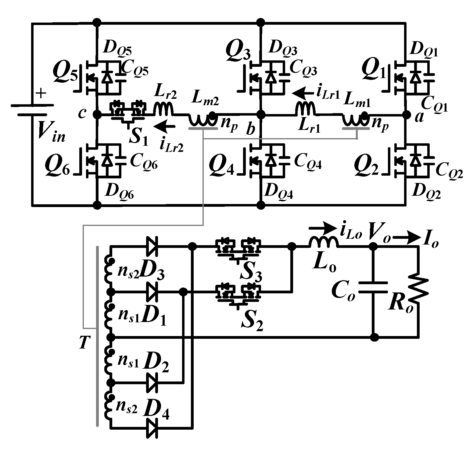
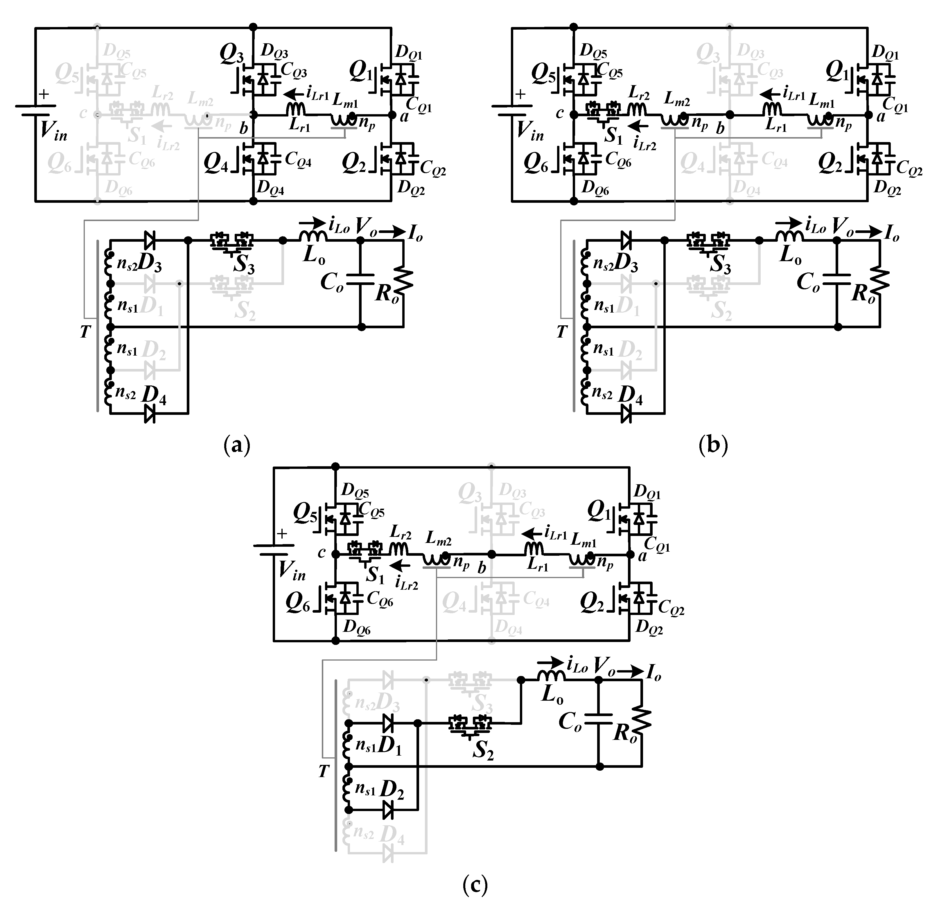
The proposed circuit topology is provided in Figure 1. As can be noted, three converter legs and one AC switch (two MOSFETs (metal–oxide–semiconductor field-effect transistor) connected by a back-to-back structure) are used on the input-side, and two sets of secondary winding turns and two AC switches are used on the output-side. The magnetic transformer with two primary turns np and two different secondary turns ns1 and ns2 is used in the proposed circuit topology. Switch S1 is on or off to select the full-bridge circuit with the larger primary turns 2np (S1 on, Q3 and Q4 off) or less primary turns np (S1, Q5, and Q6 off) on the input-side. Two AC switches S2 and S3 are on/off on the output-side to select the secondary turns ns1 or ns1+ns2 connected to the output inductor. According to the on/off states of S1~S3 and Q1~Q6, the presented three-leg PWM converter has three different equivalent circuits (Figure 2) under three voltage ranges: low voltage range (Vin,min–2Vin,min), medium voltage range (2Vin,min–4Vin,min), and high voltage range (4Vin,min–8Vin,min). For low voltage operation, the equivalent circuit is given in Figure 2a. It can be seen that switches S1, S2, Q5, and Q6 are off and S3 is on. Since the phase-shift PWM scheme is adopted to generate the PWM signals of Q1 ~ Q4, the equivalent full-bridge converter (Q1~Q4, Lr1, T, D3, D4, Lo, and Co) with transformer turns-ratio NL = np/(ns1 + ns2) is operated to achieve high voltage gain GL = Vo/Vin.L = 2deff/NL, where Vin.L denotes Vin in the low input voltage range and deff is the effective duty cycle of the full-bridge converter. Figure 2b gives the equivalent circuit of the proposed converter under the medium input voltage range Vin.M = 2Vin,min–4Vin,min. Q3, Q4, and S2 are in the off-state, and S1 and S3 are in the on-state. The equivalent circuit with components Q1, Q2, Q5, Q6, Lr1, Lr2, D3, D4, Lo, Co, and T with turns-ratio NM = 2np/(ns1+ns2) is adopted for the medium voltage range to achieve the low voltage gain GM = Vo/Vin.M = 2deff/NM. Figure 2c provides the equivalent circuit for high voltage range operation (Vin,H = 4Vin,min–8Vin,min). The switches Q3, Q4, and S3 are in the off-state, and S1 and S2 are in the on-state. The equivalent circuit shown in Figure 2c has voltage gain GH = Vo/Vin.H = 2deff/NH, where NH = 2np/ns1. According to the above discussion, the proposed converter can be operated at three different input voltage ranges by proper selection of the on/off states of Q1–Q6 and S1–S3 to achieve wide voltage operation from Vin,min to 8Vin,min.
3. The Principle of Operation
3.1. Low Voltage Operation (S3 on; Q5, Q6, S1, S2 off)
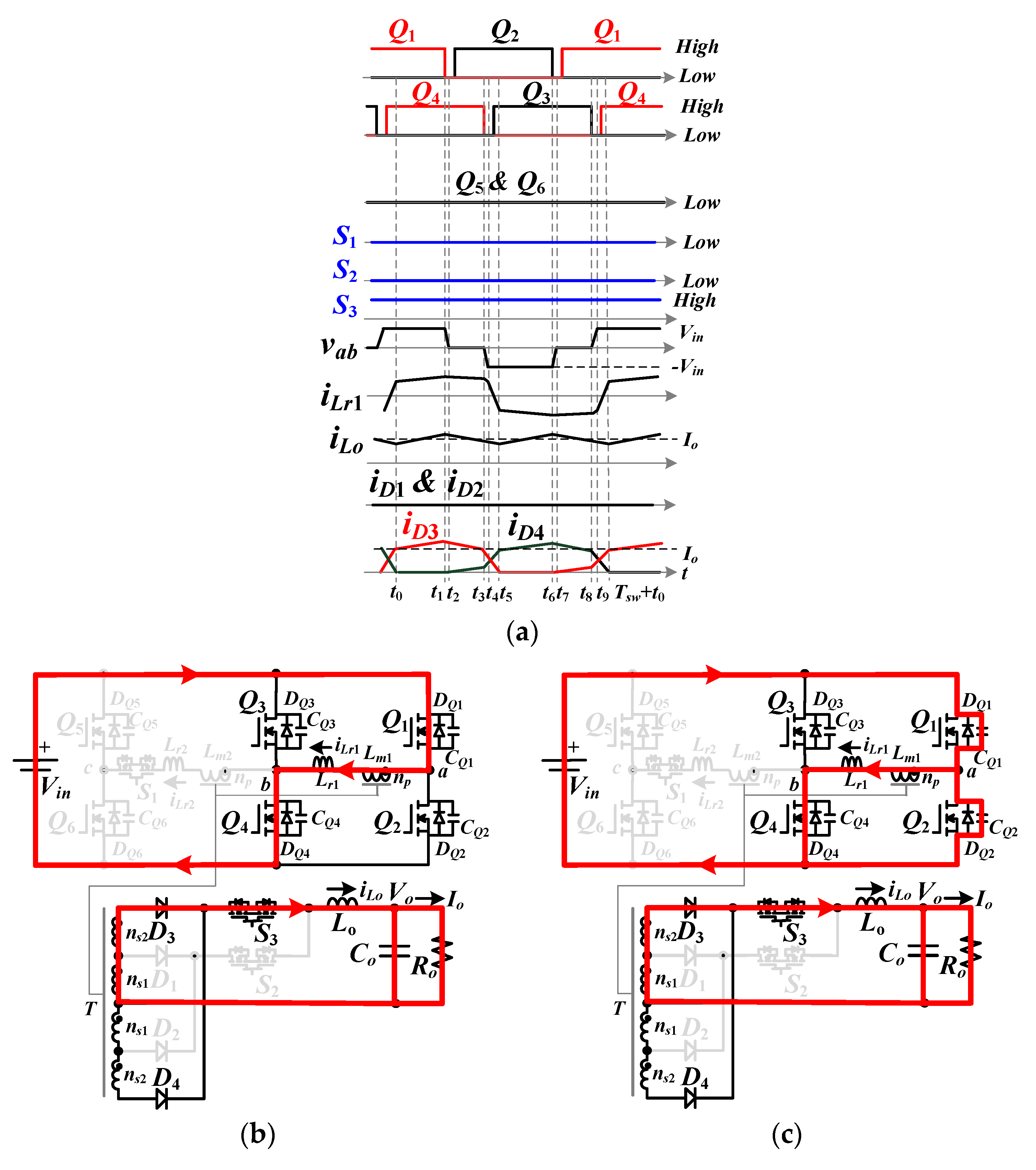
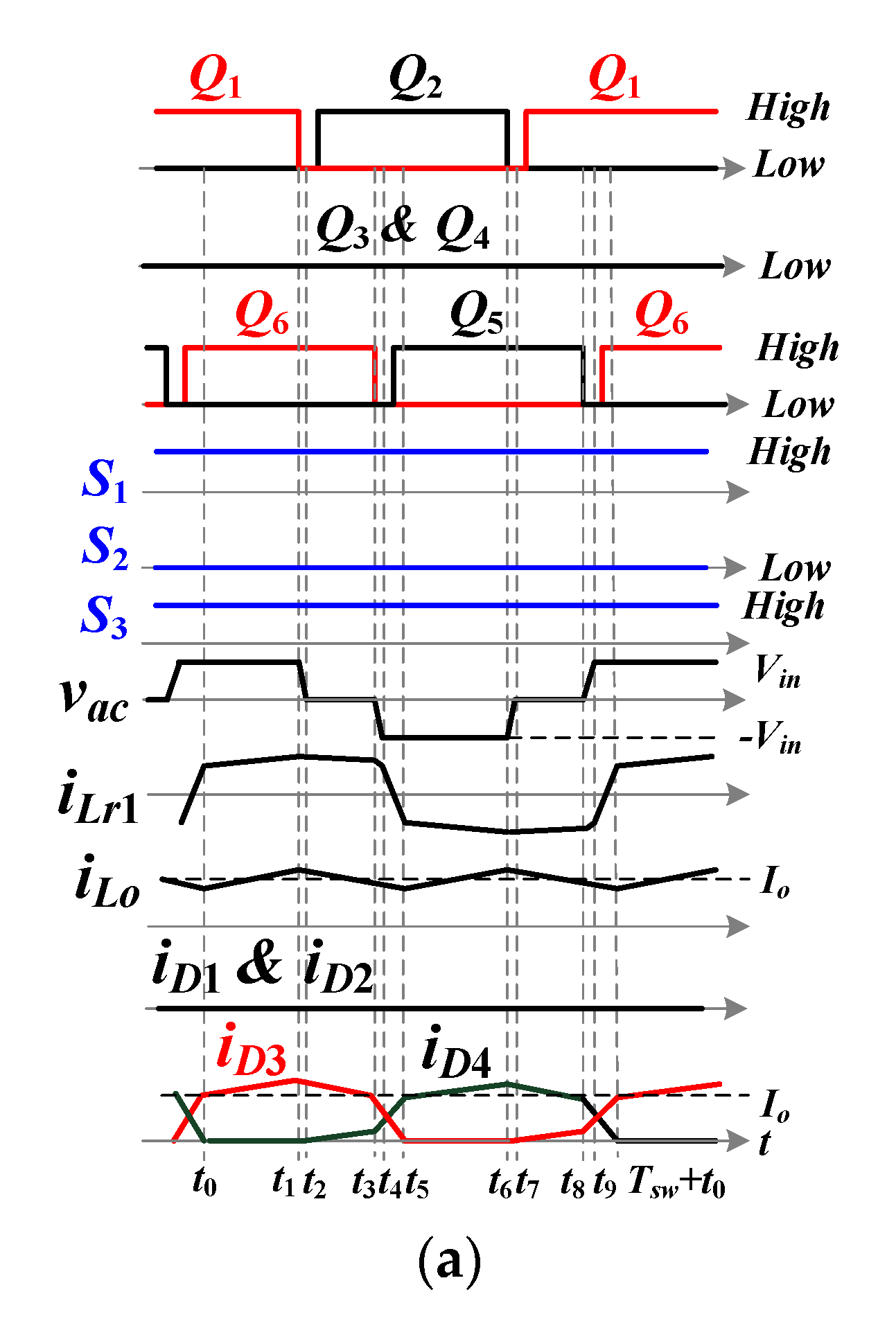
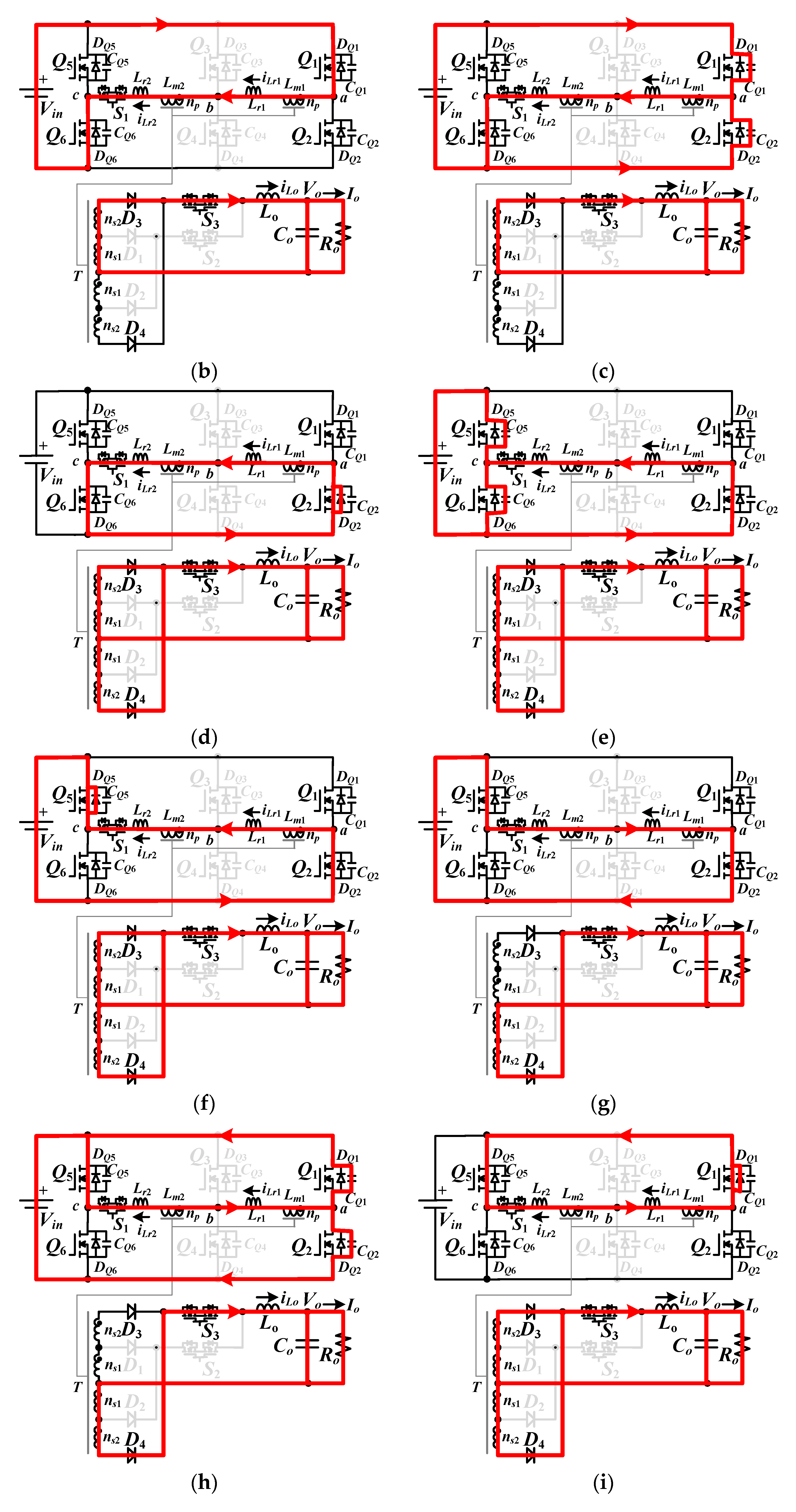
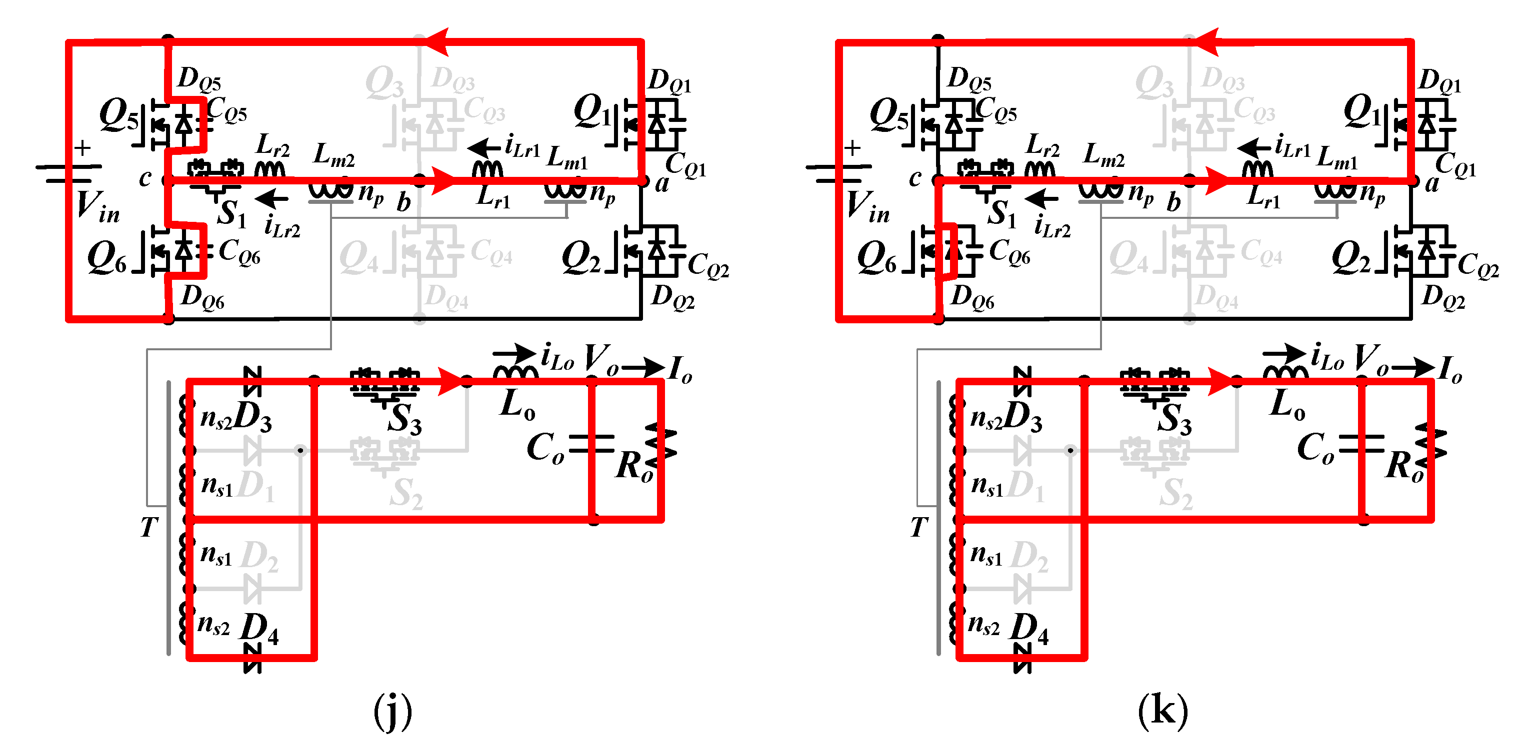
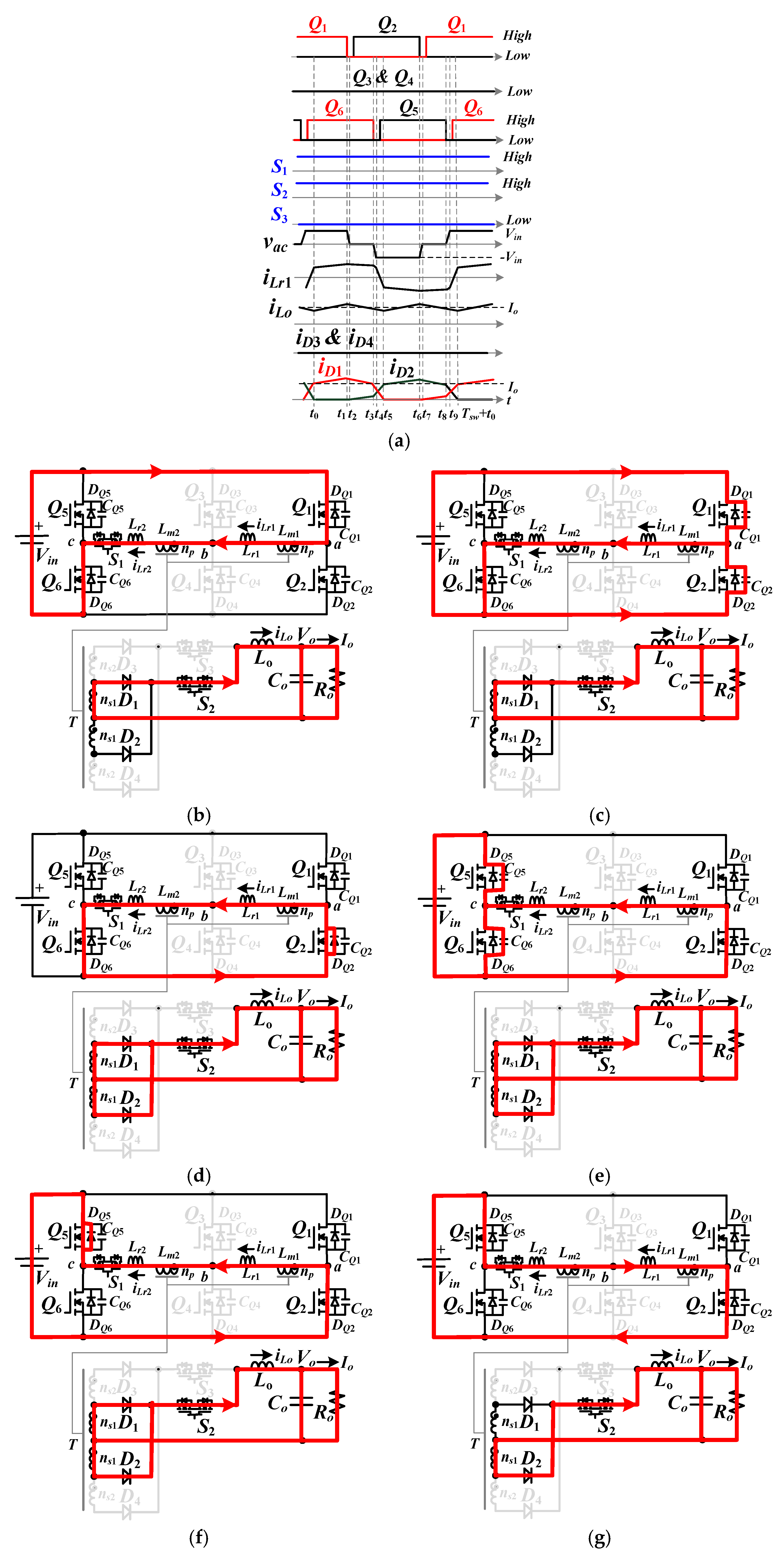
When Vin,min ≤ Vin < 2Vin,min, the active switches Q5, Q6, S1, and S2 are off and S3 is on. The proposed converter has np primary winding turns and ns1 + ns2 secondary winding turns in Figure 2a. In the presented circuit, it is assumed that Lm1 and Lm2 ≫ Lr1 and Lr2, CQ1 = … = CQ6 = Coss, and ns1 = ns2. Figure 3a demonstrates the main voltage and current waveforms under low voltage operation. The voltage gain of the presented converter for low voltage operation is GL = 2deff/NL = 4ns1deff/np. There are ten operation modes in every one switching period. Figure 3b–k gives these ten equivalent operating circuits. Since the PWM waveforms are symmetrical between Modes 1–5 and Modes 6–10, only the circuit operations of Modes 1–5 are examined in the following discussion.
Mode 1 [t0, t1]: Mode 1 begins at t = t0 when Q1 and Q4 (Q2 and Q3) are active (inactive) on the input-side and D3 conducts on the output-side. The input current flows through the components Q1, T, Lr1, and Q4, and the output current flows through the components T, D3, Lo, and Co. The magnetizing voltage vLm1 ≈ Vin (due to Lm1 ≫ Lr1) and vLo ≈ Vin/NL − Vo. Thus, iLr1 and iLo are calculated as:
Therefore, iLr1 and iLo increase in Mode 1, and vCQ2 = vCQ3 = Vin and vD4 = 2Vin/NL.
Mode 2 [t1, t2]: Mode 2 begins at t1 when Q1 turns off. The primary current iLr1 at time t1 is positive. Therefore, the output capacitors CQ1 and CQ2 of switches Q1 and Q2 charge from 0 V and discharged from Vin, respectively. If the inductor energy is greater than the capacitor energy 2, then the capacitor CQ2 is discharged to zero voltage at t = t2. The time interval of this mode is given in Equation (3).
The dead time td between the PWM signals of Q1 and Q2 must be greater than Δt12 to accomplish the soft switching turn-on of Q2.
Mode 3 [t2, t3]: The inductor current iLr1 > 0, and vCQ2 = 0 at t2. The body diode DQ2 of switch Q2 is conducting, and Q2 can be turned on after time t2 to achieve soft switching turn-on. The primary current iLr1 is flowing the components Q2, T, Lr1, and Q4, and vLm1 = 0. The secondary-side diodes D3 and D4 are both conducting, vLo = −Vo, and iLo decreases in this mode. The inductor currents are given as:
where VQ2,drop and VQ4,drop are the voltage drop on switches Q2 and Q4, respectively. The diode currents iD3 (iD4) decrease (increase), and the slopes of the diode currents are calculated as:
Mode 4 [t3, t4]: Mode 4 starts at time t3 when the lagging switch Q4 turns off. The primary current iLr1 at time t3 is positive. Therefore, the output capacitor CQ3 (CQ4) of switch Q3 (Q4) is discharged (charged) from Vin (0V). Due to D3 and D4 conducting in Mode 4, it can obtain vLm1 = 0. If the inductor energy is greater than the energy 2, then it can obtain vCQ3(t4) = 0. The time interval of this mode is given in Equation (7).
The dead time td between the PWM signals of Q3 and Q4 must be greater than Δt34 to accomplish soft switching turn-on of Q3.
Mode 5 [t4, t5]: At t = t4, iLr1 > 0, and vCQ3 = 0. The body diode DQ3 of the lagging-leg switch Q3 is forward biased. After time t4, Q3 turns on under zero voltage. The D3 and D4 are still conducting in this mode. The leg voltage vab = −Vin and the inductor voltage vLr1 ≈ −Vin, so that iLr1 decreases. In Mode 5, iD3 (iD4) decreases (increases). The slopes of iD3 and iD4 are expressed as:
The diode current iD3 is decreased to zero at time t5, and the time duration of Mode 5 is calculated as:
The duty cycle loss in this mode is obtained as:
where Tsw is the switching period of PWM waveforms. After the time t5, the converter operation goes to the next half switching period.
3.2. Medium Voltage Operation (S1, S3 on; Q3, Q4, S2 off)
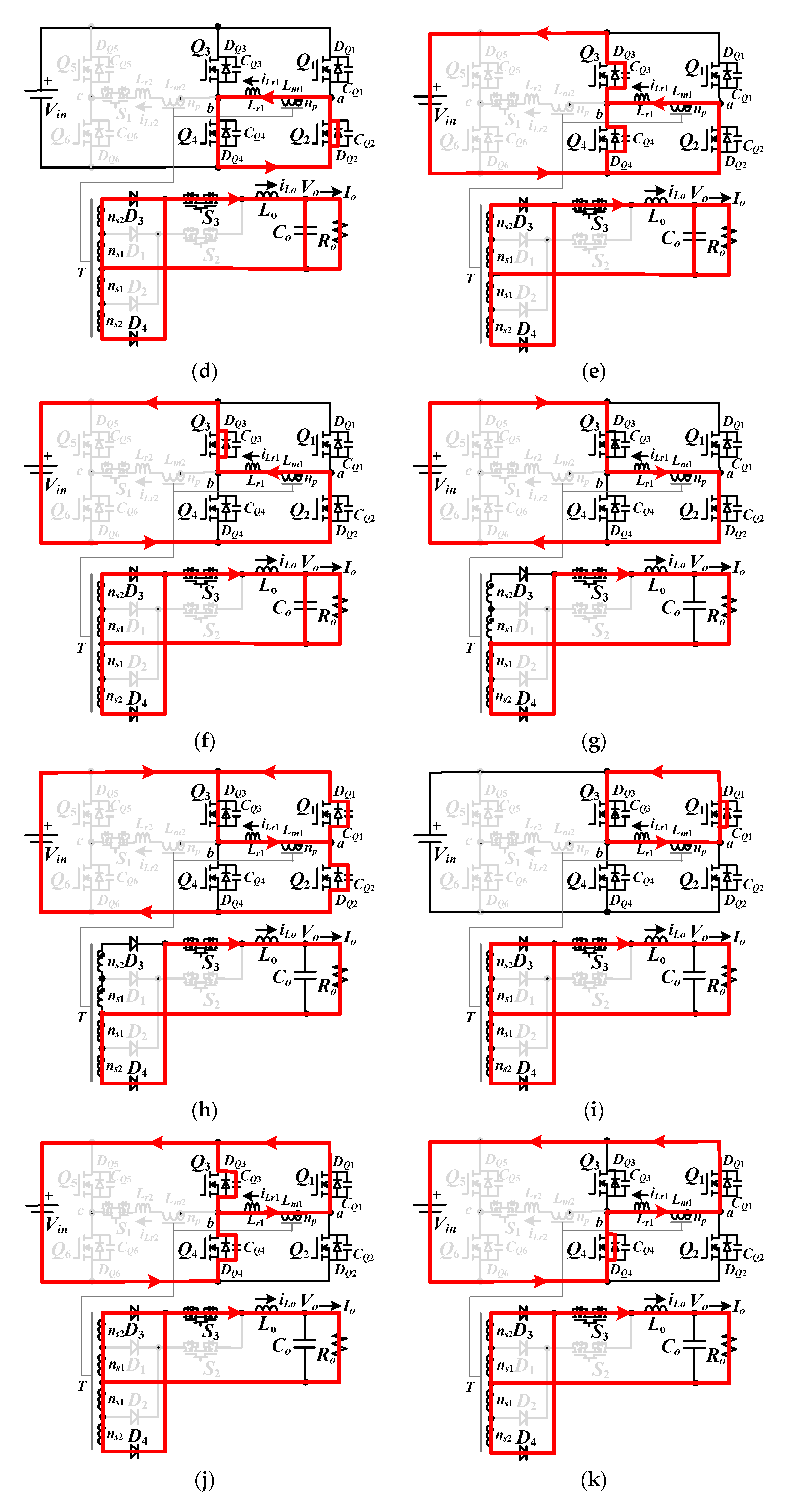
When Vin is in the medium voltage range (2Vin,min ≤ Vin < 4Vin,min), S1 and S3 are in the on-state and Q3, Q4, and S2 are in the off-state (Figure 2b). The proposed converter has 2np primary winding turns and ns1 + ns2 secondary winding turns in Figure 2b. The voltage gain for medium voltage operation is GM = 2deff/NM = 2ns1deff/np. Comparing the voltage gains GL and GM, it can be noted that GL = 2GM. Figure 4a demonstrates the main voltage and current waveforms under medium voltage operation. There are ten operation modes in every one switching period. Figure 4b–k gives these ten equivalent operating circuits. Since the PWM waveforms are symmetrical for each half switching cycle, only the circuit operations of Modes 1–5 are discussed in the following.
Mode 1 [t0, t1]: Q1, Q6, and D3 conduct at time t0. The input current flows through Q1, T, Lr1, Lr2, and Q6, and the output current flows through T, D3, Lo, and Co. The magnetizing voltage vLm1 + vLm2 ≈ Vin due to Lm1 + Lm2 ≫ Lr1 + Lr2. Since vLo ≈ Vin/NM − Vo > 0, iLr1 and iLo both increase linearly, and iLr1(t) = iLr2(t) ≈ iLo(t)/NM. The drain-to-source voltages of Q2 and Q5 are equal to Vin, and the diode voltage vD4 = 2Vin/NM.
Mode 2 [t1, t2]: At time t = t1, the leading-leg switch Q1 is turned off. iLr1 is positive, and CQ2 is discharged from Vin. If the inductor energy at time t1 is greater than the capacitor energy 2, then CQ2 can be discharged to zero voltage at time t2.
Mode 3 [t2, t3]: Since vCQ2(t2) = 0 and iLr1(t2) > 0, the body diode DQ2 conducts, and the leading-leg switch Q2 can be turned on under zero voltage. The leg voltage vac = 0 and the primary-side and secondary-side voltages of transformer T are zero voltage. Thus, D3 and D4 both conduct. Therefore, vLo equals −Vo, and iLo is decreasing.
Mode 4 [t3, t4]: Since Q6 is turned off at time t3 and iLr1(t3) > 0, CQ5 is discharged. The magnetizing voltages vLm1 = vLm2 = 0. If the inductor energy > , then vCQ5 will reach zero voltage at time t4.
Mode 5 [t4, t5]: Since vCQ5(t4) = 0 and iLr1(t4) > 0, the body diode DQ5 conducts, and Q5 can turn on at t4 under zero voltage. In this mode, vac = −Vin and vLm1 = vLm2 = 0 due to D3 and D4 conducting. vLr1 + vLr2 = −Vin, and iLr1 decreases. At time t5, iD3 is decreased to zero. Then, the converter operation goes to the next half switching period.
3.3. High Voltage Operation (S1, S2 on; Q3, Q4, S3 off)
When 4Vin,min < Vin < 8Vin,min, S1 and S2 are turned on and Q3, Q4 and S3 are turned off (Figure 2c). This equivalent circuit has 2np primary turns and ns1 secondary turns, and the voltage gain GH = 2deff/NH = ns1deff/np. Comparing the voltage gains GL, GM, and GH, it can be noted that GL > GM > GH. Figure 5a demonstrates the main voltage and current waveforms under high voltage operation. Figure 5b–k gives these ten equivalent operating circuits. Since the PWM waveforms are symmetrical for each half switching cycle, only the circuit operations of Modes 1–5 are discussed in the following.
Mode 1 [t0, t1]: At t = t1, D1, Q1 and Q6 conduct. iLr1 flows through Q1, T, Lr1, Lr2, and Q6 on the primary-side of transformer T. iLo flows through D1, Lo, and Co on the secondary-side of T. Since vLo ≈ Vin/NH − Vo > 0, iLr1 and iLo both increase linearly in this mode. The drain-to-source voltages vCQ2 = vCQ5 = Vin, and the diode voltage vD2 = 2Vin/NH.
Mode 2 [t1, t2]: Q1 turns off at time t1. Due to iLr1 being positive, iLr1 discharges CQ2 from Vin. If the inductor energy at t1 is greater than the capacitor energy 2, then vCQ2 will be decreased to zero voltage at t2.
Mode 3 [t2, t3]: Since vCQ2(t2) = 0 and iLr1(t2) > 0, the body diode DQ2 is forward biased. Thus, the leading-leg switch Q2 turns on at time t2 under zero voltage. In this mode, vac = 0, and the primary winding and secondary winding voltages equal zero voltage. The diodes D1 and D2 both conduct so that vLo equals −Vo and iLo is decreased.
Mode 4 [t3, t4]: At time t3, the lagging-leg switch Q6 turns off. iLr1(t3) discharges CQ5 from Vin. Since D3 and D4 still conduct, it can obtain vLm1 = vLm2 = 0. If the energy > , then VCQ5 = 0 at the end of this mode.
Mode 5 [t4, t5]: At time t4, vCQ5 = 0. iLr1(t4) > 0, and the body diode DQ5 conducts. The lagging-leg switch Q5 can be turned on at time t4 under zero voltage. Since vac = −Vin and vLm1 = vLm2 = 0, iLr1 is decreased. At t5, iD1 = 0. Then, the converter operation goes to the next half switching period.
4. Converter Characteristics and Design Considerations
According to the different turns-ratio of the transformer, the presented converter has three equivalent circuits. Three back-to-back MOSFETs are used in the presented circuit to have wide input voltage operation. Based on the flux balance on the output inductor, the load voltage is calculated in Equation (11).
The average diode currents ID1 = … = ID4 = Io/2. The voltage ratings of D1 ~ D4 are VD1,rating = VD2,rating = (Vin,maxns1)/np and VD3,rating = VD4,rating = Vin,max(ns1 + ns2)/np. The voltage ratings of Q1 ~ Q6 and S1 ~ S3 are VQ1,rating = … = VQ6,rating = Vin,max, VS1,rating = Vin,maxns2/(2np), and VS2,rating = VS3,rating = Vin,maxns2/(2np). The average switch currents IS2,av = IS2,av = Io. If the maximum duty cycle loss in Equation (10) is given, then the maximum primary inductances Lr1 and Lr2 are derived as:
The inductance Lo is derived in Equation (13) under the maximum input voltage and minimum effective duty cycle.
A 420 W prototype is illustrated as a design example to obtain the circuit parameters. The operating low input voltage range Vin,L is from 30 V to 60 V; the medium input voltage range Vin,M is from 60 V to 120 V; and the high voltage range Vin,H is from 120 V to 240 V. The output voltage Vo is 12 V. The PWM switching frequency of Q1–Q6 is 100 kHz. If 30 V ≤ Vin < 60 V, S1, S2, Q5, and Q6 are off and S3 is on. The voltage gain of the converter is GL = 4deffnS1/np. If 60 V ≤ Vin < 120 V, S2, Q3, and Q4 are off and S1 and S3 are on. The voltage gain of the converter is GM = 2deffnS1/np. If 120 V ≤ Vin < 240 V, S3, Q3, and Q4 are off and S1 and S2 are on. The voltage gain of the proposed circuit is GH = deffnS1/np. In order to prevent the control signal oscillation at the transition voltages 60 V and 120 V, the Schmitt trigger circuits with ±5 V voltage tolerance are used between three input voltage ranges. Thus, the actual voltage ranges are Vin,L = 30 V–65 V, Vin,M = 55 V–125 V, and Vin,H = 115 V–240 V. The circuit efficiency is assumed 90% at minimum input voltage and full road condition, and the maximum duty cycle dmax and maximum duty cycle loss dloss,5,max are assumed to be 0.45 and 0.15, respectively, at minimum input voltage. Therefore, the maximum effective duty cycle deff,max = dmax – dloss,5,max = 0.3. The primary inductances Lr1 and Lr2 can be estimated as:
From Equation (11), the turns-ratio NL is calculated as:
In the laboratory prototype, the primary and secondary turns of transformer T are np = 12 and ns1 = ns2 = 4. The magnetizing inductances Lm1 = Lm2 = 820 µH. Under the low input voltage range, it can obtain the minimum effective duty cycle deff,min in Equation (16) at Vin = 65 V.
The assumed ripple current ΔiLo = 3.5 A (10% of the rated load current) at Vin,L,max = 65 V. The output inductance Lo is obtained as:
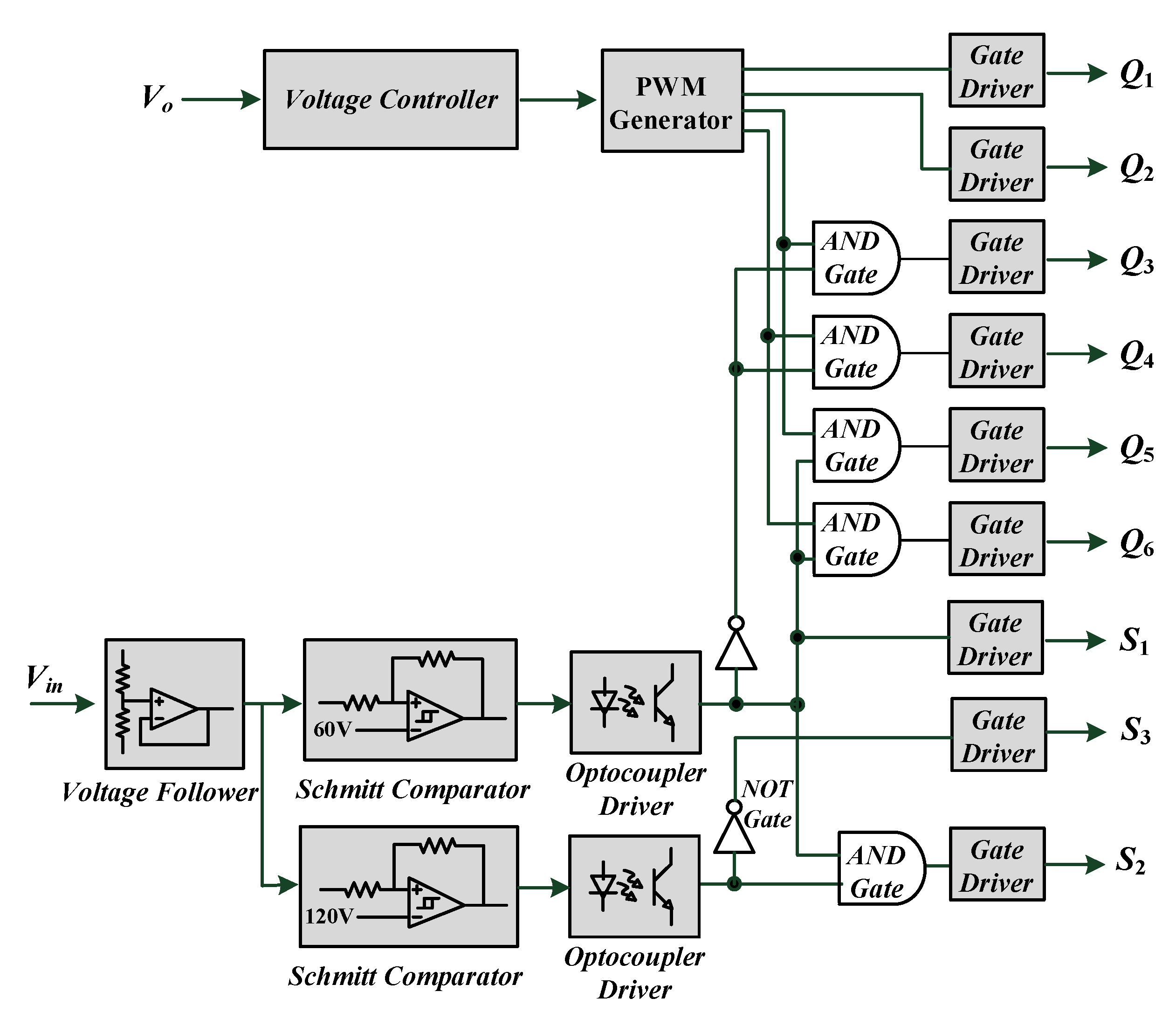
The output inductance Lo = 20 µH is used in the prototype circuit. The maximum root-mean-squared (rms) currents of Q1 ~ Q6 are approximated as . The maximum rating voltage of Q1–Q6 is equal to Vin,max = 240 V. Therefore, the MOSFETs IXTN80N30L2 with the 300 V/80 A/30 mΩ rating are used for switches Q1–Q6 and S1. The MOSFETs STD100N10F7 with 100 V/80 A/6.8 mΩ ratings are used for switches S2 and S3. The synchronous rectifiers MOSFETs IXFH80N25X3 with 250 V/80 A/16 mΩ ratings are used for diodes D1–D4 to further reduce conduction losses. The output capacitance Co = 470 µF/35V. The PWM generator UCC3895 is used to provide the PWM waveforms for Q1–Q6. The voltage regulator TL431 is used to regulate load voltage. The Schmitt comparators and logic gates are used to produce the on/off signals of S1–S3. Figure 6 provides the control blocks in the prototype circuit.
5. Experimental Verifications
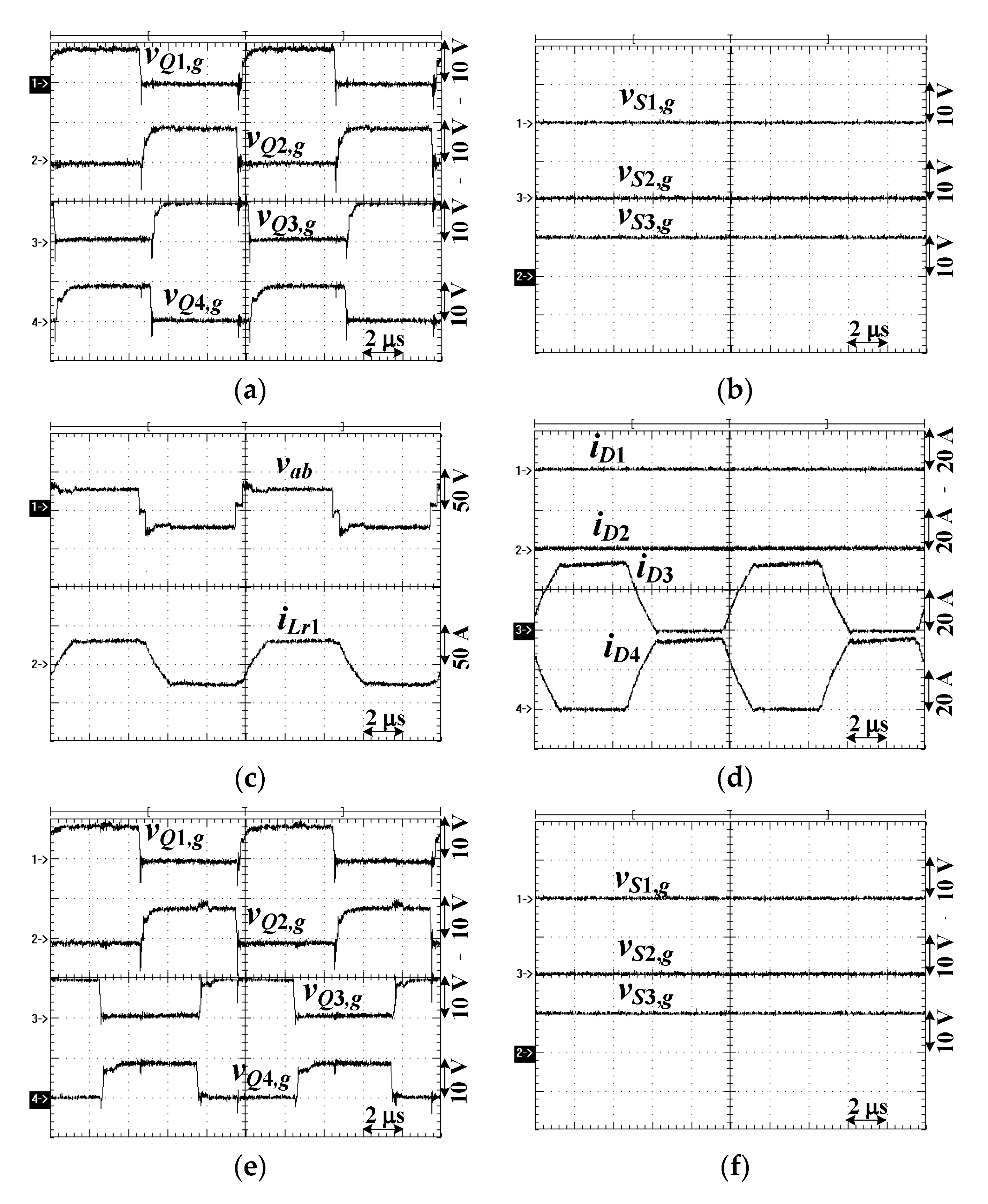
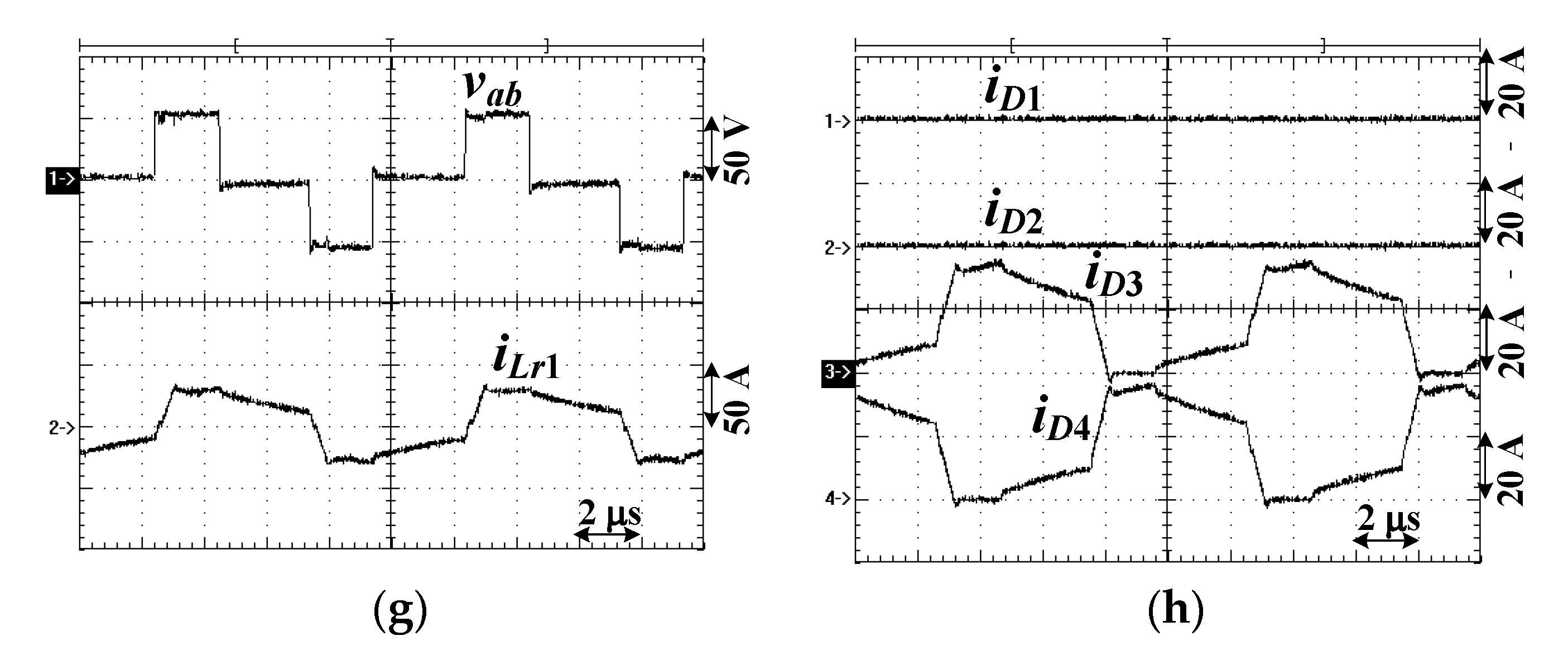
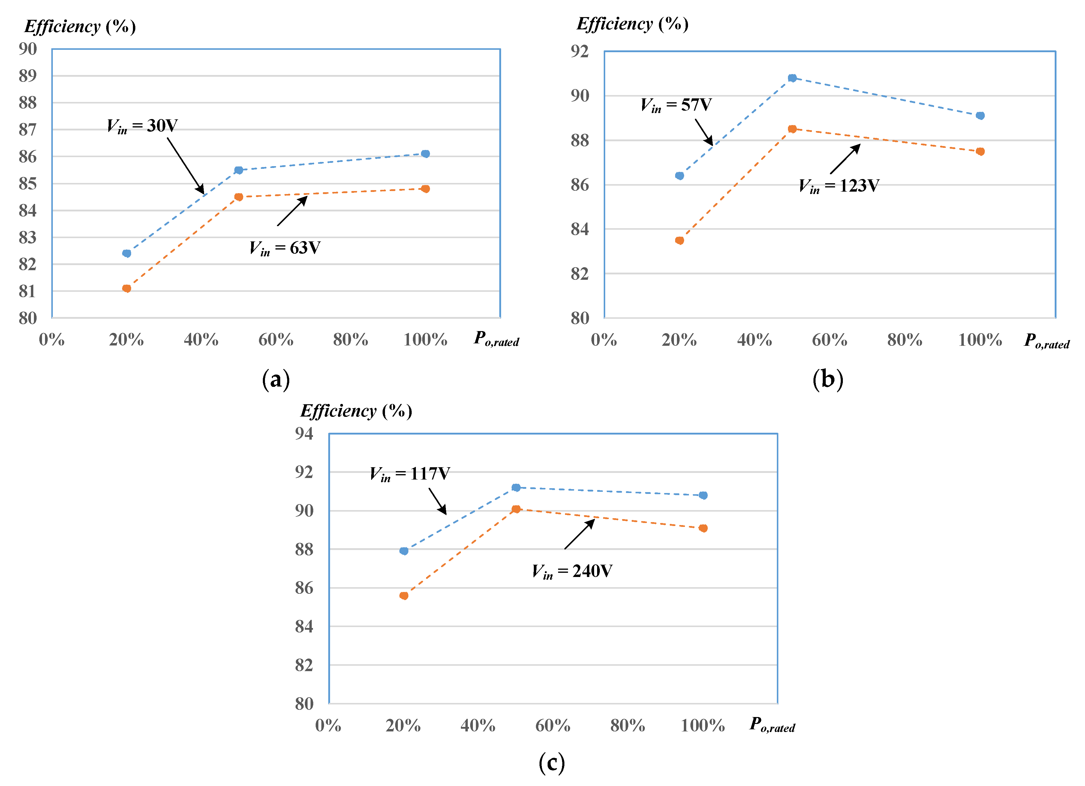
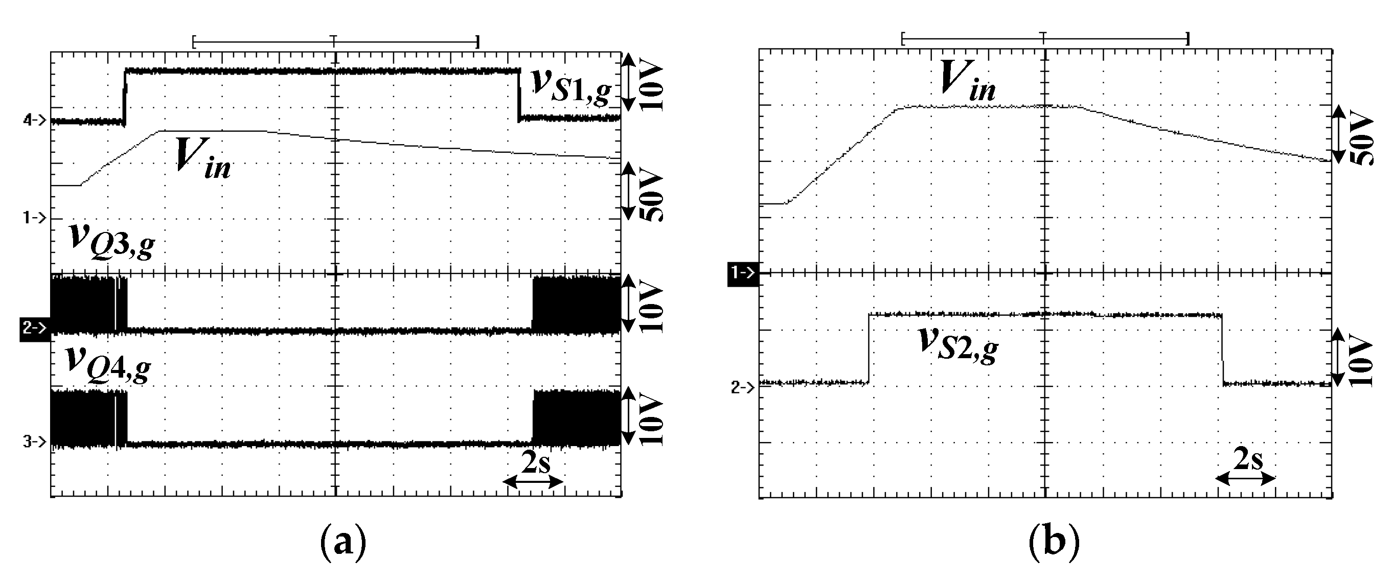
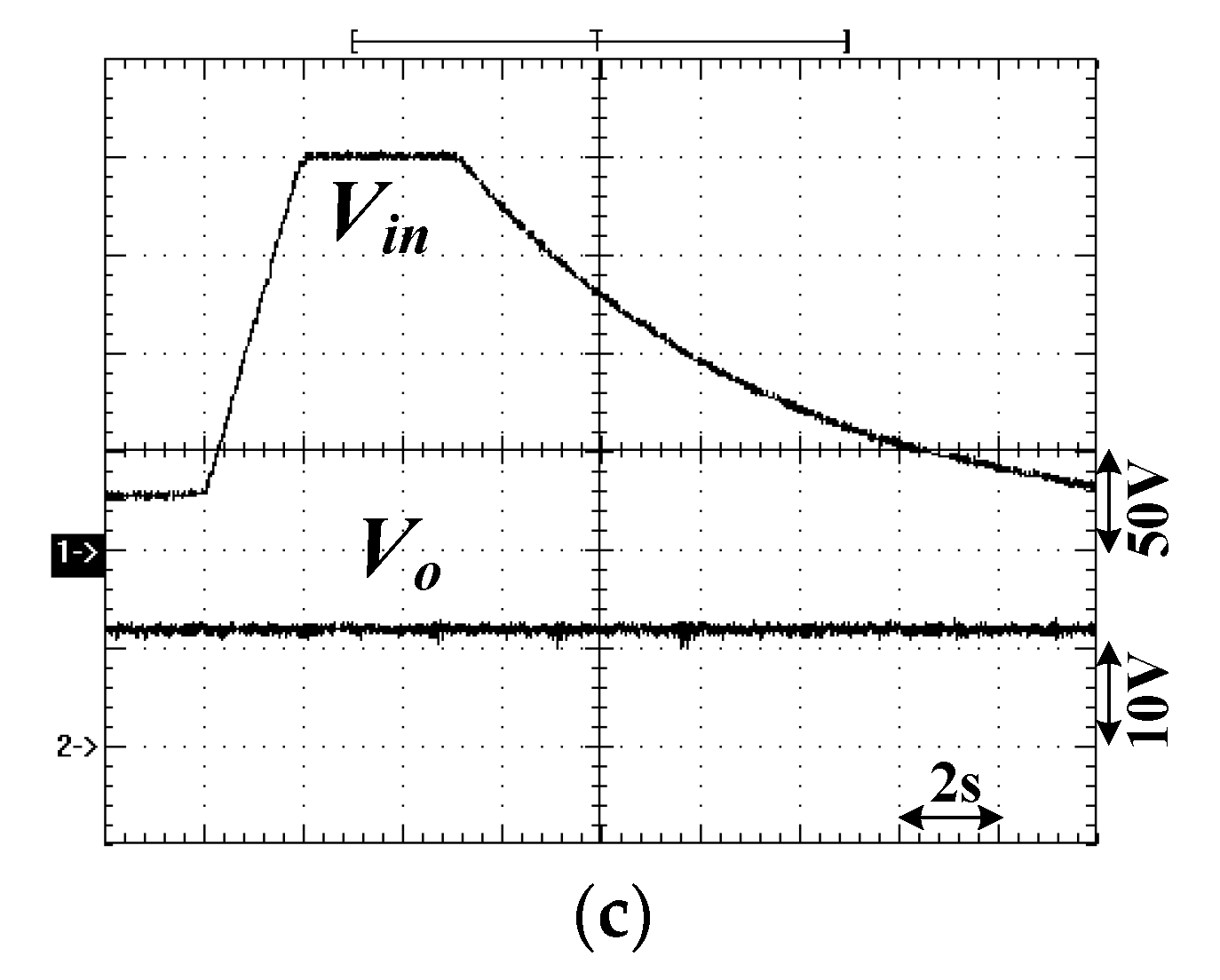
The components of the prototype circuit were obtained in the previous section. The experimental results are verified in this section to demonstrate the converter effectiveness. Figure 7 demonstrates the test waveforms for low voltage operation. The PWM waveforms vQ1,g – vQ4,g at Vin = 30 V are provided in Figure 7a. The gate voltages of AC switches S1–S3 under Vin = 30 V are given in Figure 7b. One can observe that S1 and S2 are off and S3 is on. Therefore, only the full-bridge converter with Q1–Q4 and diodes D3 and D4 are operated. Figure 7c provides the experimental results of vab and iLr1 under Vin = 30 V input. The secondary-side diode currents at Vin = 30 V are shown in Figure 7d. It can be obtained that D1 and D2 are in the off-state in the low input voltage operation. Similarly, the PWM waveforms vQ1,g – vQ4,g, vS1,g – vS3,g, vab, iLr1, and iD1 – iD4 at Vin = 63 V input are demonstrated in Figure 7e–h. From the test results in Figure 7c,g, one can observe that the leg voltage vab has a large duty cycle at Vin = 30 V compared to Vin = 63 V. Therefore, the output inductor current iLo has less ripple current ΔiLo at 30 V input voltage than 63 V input voltage. This large ripple current at 63 V input can be observed in iLr1 in Figure 7g and iD3 and iD4 in Figure 7h. Figure 8 provides the measured waveforms of the converter for the medium voltage range operation and the rated power. For the medium input voltage range, S1 and S3 are conducting, S2, Q3, and Q4 are turned off, and D1 and D2 are reverse biased. The gate voltages vQ1,g, vQ2,g, vQ5,g, and vQ6,g are given in Figure 8a, and the gate voltages of S1–S3 are shown in Figure 8b under Vin = 57 V. The measured waveforms of vac, iLr1, and iD1 – iD4 are demonstrated in Figure 8c,d under Vin = 57 V. Similarly, the measured waveforms of Q1, Q2, Q5, Q6, S1–S3, vac, iLr1, and iD1 ~ iD4 are provided in Figure 8e–h under Vin = 123 V. The measured results for the high voltage range are provided in Figure 9. For the high voltage range operation, S1 and S2 are on, S3 is off, PWM switches Q3 and Q4 are off, and D3 and D4 are off. The turns-ratio 2np/ns1 of the transformer T is operated in the high input voltage range. Figure 9a–d gives the test results of Q1, Q2, Q5, Q6, S1–S3, vac, iLr1, and iD1 ~ iD4 at Vin = 117 V. Similarly, the measured waveforms under Vin = 240 V are demonstrated in Figure 9e–h. The measured waveforms of Q1 (leading-leg switch) are illustrated in Figure 10. From the test results in Figure 10, it is clear that the leading-leg switch Q1 has the zero voltage switching turn-on characteristic from minimum to maximum input voltage and from 20% power to the rated power. Figure 11 gives the measured waveforms of Q3 (lagging-leg switch) under 30 V input and 50% and 100% rated power. From Figure 11, it can be observed that Q3 (lagging-leg switch) turns on under zero voltage from 50% rated power to full rated power. Q5 and Q6 are operated under medium and high input voltage ranges. Figure 12 gives the measured waveforms of Q5 (lagging-leg switch) under Vin = 240 V and 50% and 100% rated power. One can observe that the leading-leg switch Q5 turns on under zero voltage from 50% rated power to full rated power. Figure 13 demonstrates the measured efficiencies for different voltage ranges. Compared to the high input voltage range, the converter has large primary current and conduction losses under low input voltage range. Figure 14a gives the test results of the input voltage Vin and the switching signals vQ3,g and vQ4,g between Vin = 30 V and Vin = 80 V under full load operation. When 30 V < Vin < 60 V, the converter is operated in the low input voltage range. The switches Q3 and Q4 are activated, and switch S1 is off. When Vin > 60 V and < 80 V, the converter is operated at the medium input voltage range. Therefore, S1 is on, and Q3 and Q4 are off. Figure 14b provides the test results of Vin and S2 between Vin = 65 V and Vin = 150 V under full load operation. When Vin is increased from 65 V and greater than 120 V, the switch S2 is turned on. Then, the converter is operated under the high input voltage range. If the Vin is decreased from 150 V and less than 120 V, the switch S2 is turned off, and the converter is operated under the medium input voltage range. Figure 14c shows the test waveforms of input and output voltages under full load. The input voltage is variated between 30 V (low input voltage range) and 200 V (high input voltage range). It is obvious that the load voltage is stable at 12 V output voltage.
6. Conclusions
To overcome the limited input voltage range operation of conventional PWM converters for solar power conversion, a novel three-leg PWM converter with an adjustable transformer turns-ratio was proposed and implemented to realize soft switching turn-on with wide input voltage operation. According to the input voltage range, the proposed three-leg converter had two equivalent circuits with variable primary winding turns on the input-side. On the secondary-side, the proposed converter also had two equivalent circuits by using variable secondary winding turns to achieve different voltage gains. Thus, the proposed three-leg converter had three equivalent circuits operated at different input voltage ranges to provide a stable DC output voltage. Each equivalent circuit using PWM operation could be operated to achieve 2:1 input voltage range operation. Thus, the proposed circuit could realize 8:1 (Vin,in ~ 8Vin,min) wide input voltage range operation. The Schmitt voltage comparators were adopted to generate the signals of the three voltage range selection. The proposed three-leg converter could work as the first stage of photovoltaic (PV) power converters with a wide range of voltage variation. Experiments from a laboratory prototype confirmed the theoretical converter characteristics with wide voltage range operation.
Author Contributions
Conceptualization, methodology, formal analysis, writing—review and editing, B.-R.L.; data curation, J.-W.C. Both authors have read and agreed to the published version of the manuscript.
Funding
This research is funded by the Ministry of Science and Technology, Taiwan, under Grant Number MOST 108-2221-E-224-022-MY2.
Acknowledgments
This research is supported by the Ministry of Science and Technology, Taiwan, under Contract MOST 108-2221-E-224-022-MY2.
Conflicts of Interest
The authors declare no conflict of interest.
References
- Lin, B.R. Implementation of a parallel-series resonant converter with wide input voltage range. Energies 2019, 12, 4095. [Google Scholar] [CrossRef] [Green Version]
- Lin, B.R.; Dai, C.X. Wide Voltage Resonant Converter Using a Variable Winding Turns Ratio. Electronics 2020, 9, 370. [Google Scholar] [CrossRef] [Green Version]
- Zhang, Y.; Fu, C.; Sumner, M.; Wang, P. A wide input-voltage range quasi-Z-source boost DC–DC converter with high-voltage gain for fuel cell vehicles. IEEE Trans. Ind. Electron. 2018, 65, 5201–5212. [Google Scholar] [CrossRef] [Green Version]
- Wang, H.; Nayar, C.; Su, J.; Ding, M. Control and interfacing of a grid-connected small-scale wind turbine generator. IEEE Trans. Energy Convers. 2011, 26, 428–434. [Google Scholar] [CrossRef]
- Wang, P.; Zhou, L.; Zhang, Y.; Li, J.; Sumner, M. Input-parallel output-series DC-DC boost converter with a wide input voltage range, for fuel cell vehicles. IEEE Trans. Veh. Technol. 2017, 66, 7771–7781. [Google Scholar] [CrossRef]
- Xia, Y.Y.; Fletcher, J.E.; Finney, S.J.; Ahmed, K.H.; Williams, B.W. Torque ripple analysis and reduction for wind energy conversion systems using uncontrolled rectifier and boost converter. IET Renew. Power Gener. 2011, 5, 377–386. [Google Scholar] [CrossRef]
- Jeong, Y.; Kim, J.K.; Lee, J.B.; Moon, G.W. An asymmetric half-bridge resonant converter having a reduced conduction loss for DC/DC power applications with a wide range of low input voltage. IEEE Trans. Power Electron. 2017, 32, 7795–7804. [Google Scholar] [CrossRef]
- Wu, H.; Wan, C.; Sun, K.; Xing, Y. A high step-down multiple output converter with wide input voltage range based on quasi two-stage architecture and dual-output LLC resonant converter. IEEE Trans. Power Electron. 2015, 30, 1793–1796. [Google Scholar] [CrossRef]
- Singh, A.K.; Das, P.; Panda, S.K. Analysis and design of SQR-based high-voltage LLC resonant dc-dc converter. IEEE Trans. Power Electron. 2017, 32, 4466–4481. [Google Scholar] [CrossRef]
- Wang, X.; Tian, F.; Batarseh, I. High efficiency parallel post regulator for wide range input DC–DC converter. IEEE Trans. Power Electron. 2008, 23, 852–858. [Google Scholar] [CrossRef]
- Li, W.; Zong, S.; Liu, F.; Yang, H.; He, X.; Wu, B. Secondary-side phase-shift-controlled ZVS DC/DC converter with wide voltage gain for high input voltage applications. IEEE Trans. Power Electron. 2013, 28, 5128–5139. [Google Scholar] [CrossRef]
- Lin, B.R. Implementation of a soft switching converter with series DC-DC circuits and single transformer. IET Proc.—Power Electron. 2019, 12, 1249–1255. [Google Scholar] [CrossRef]
- Ma, H.; Li, Y.; Chen, Q.; Zhang, L.; Xu, J. A single-stage integrated boost-LLC AC–DC converter with quasi-constant bus voltage for multichannel LED street-lighting applications. IEEE J. Emerg. Sel. Top. Power Electron. 2018, 6, 1143–1153. [Google Scholar] [CrossRef]
- Sarnago, H.; Lucia, O.; Burdio, J.M. A versatile resonant tank identification methodology for induction heating systems. IEEE Trans. Power Electron. 2018, 33, 1897–1901. [Google Scholar] [CrossRef]
- Wang, H.; Li, Z. A PWM LLC type resonant converter adapted to wide output range in PEV charging applications. IEEE Trans. Power Electron. 2018, 33, 3791–3801. [Google Scholar] [CrossRef]
- Lin, B.R.; Lin, G.H. Frequency-Controlled Current-Fed Resonant Converter with No Input Ripple Current. Energies 2018, 11, 413. [Google Scholar]
- Pandey, R.; Singh, B. A power-factor-corrected LLC resonant converter for electric vehicle charger using Cuk converter. IEEE Trans. Ind. Appl. 2019, 55, 6278–6286. [Google Scholar] [CrossRef]
- Lin, B.R.; Wu, G.Y. Bidirectional Resonant Converter with Half-Bridge Circuits: Analysis, Design, and Implementation. Energies 2018, 11, 1259. [Google Scholar] [CrossRef] [Green Version]
- Kim, B.; Kim, S.; Hun, D.Y.; Choi, J.H.; Kim, M. Hybrid resonant half-bridge DC/DC converter with wide input voltage range. In Proceedings of the IEEE APEC Conference, San Antonio, TX, USA, 4–8 March 2018; pp. 1876–1881. [Google Scholar]
- Lu, J.; Kumar, A.; Afridi, K.K. Step-down impedance control network resonant DC-DC converter utilizing an enhanced phase-shift control for wide-input-range operation. IEEE Trans. Ind. Appl. 2018, 54, 4523–4536. [Google Scholar] [CrossRef]
- Hu, H.; Fang, X.; Chen, F.; Shen, Z.J.; Batarseh, I. A modified high-efficiency LLC converter with two transformers for wide input-voltage range applications. IEEE Trans. Power Electron. 2012, 28, 1946–1960. [Google Scholar] [CrossRef]
Figure 1.
Circuit structure of the developed converter.

Figure 2.
Equivalent circuit of the proposed converter for (a) low voltage range, (b) medium voltage range, and (c) high voltage range.
Figure 2.
Equivalent circuit of the proposed converter for (a) low voltage range, (b) medium voltage range, and (c) high voltage range.

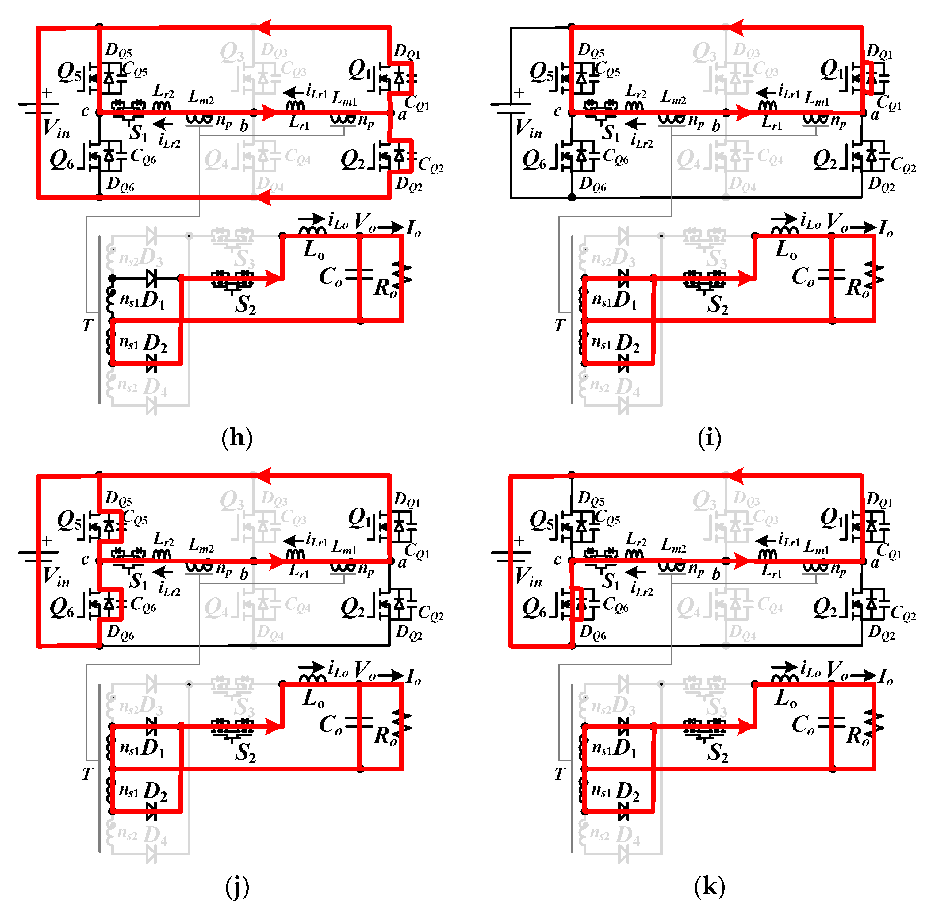
Figure 3.
PWM waveforms and equivalent circuits at low voltage range operation: (a) PWM voltage and current waveforms for (b) Mode 1, (c) Mode 2, (d) Mode 3, (e) Mode 4, (f) Mode 5, (g) Mode 6, (h) Mode 7, (i) Mode 8, (j) Mode 9, and (k) Mode 10.
Figure 3.
PWM waveforms and equivalent circuits at low voltage range operation: (a) PWM voltage and current waveforms for (b) Mode 1, (c) Mode 2, (d) Mode 3, (e) Mode 4, (f) Mode 5, (g) Mode 6, (h) Mode 7, (i) Mode 8, (j) Mode 9, and (k) Mode 10.


Figure 4.
PWM waveforms and equivalent circuits at medium voltage range operation: (a) PWM voltage and current waveforms for (b) Mode 1, (c) Mode 2, (d) Mode 3, (e) Mode 4, (f) Mode 5, (g) Mode 6, (h) Mode 7, (i) Mode 8, (j) Mode 9, and (k) Mode 10.
Figure 4.
PWM waveforms and equivalent circuits at medium voltage range operation: (a) PWM voltage and current waveforms for (b) Mode 1, (c) Mode 2, (d) Mode 3, (e) Mode 4, (f) Mode 5, (g) Mode 6, (h) Mode 7, (i) Mode 8, (j) Mode 9, and (k) Mode 10.


Figure 5.
PWM waveforms and equivalent circuits at high voltage range operation: (a) PWM voltage and current waveforms for (b) Mode 1, (c) Mode 2, (d) Mode 3, (e) Mode 4, (f) Mode 5, (g) Mode 6, (h) Mode 7, (i) Mode 8, (j) Mode 9, and (k) Mode 10.
Figure 5.
PWM waveforms and equivalent circuits at high voltage range operation: (a) PWM voltage and current waveforms for (b) Mode 1, (c) Mode 2, (d) Mode 3, (e) Mode 4, (f) Mode 5, (g) Mode 6, (h) Mode 7, (i) Mode 8, (j) Mode 9, and (k) Mode 10.


Figure 6.
Control block of the studied converter.

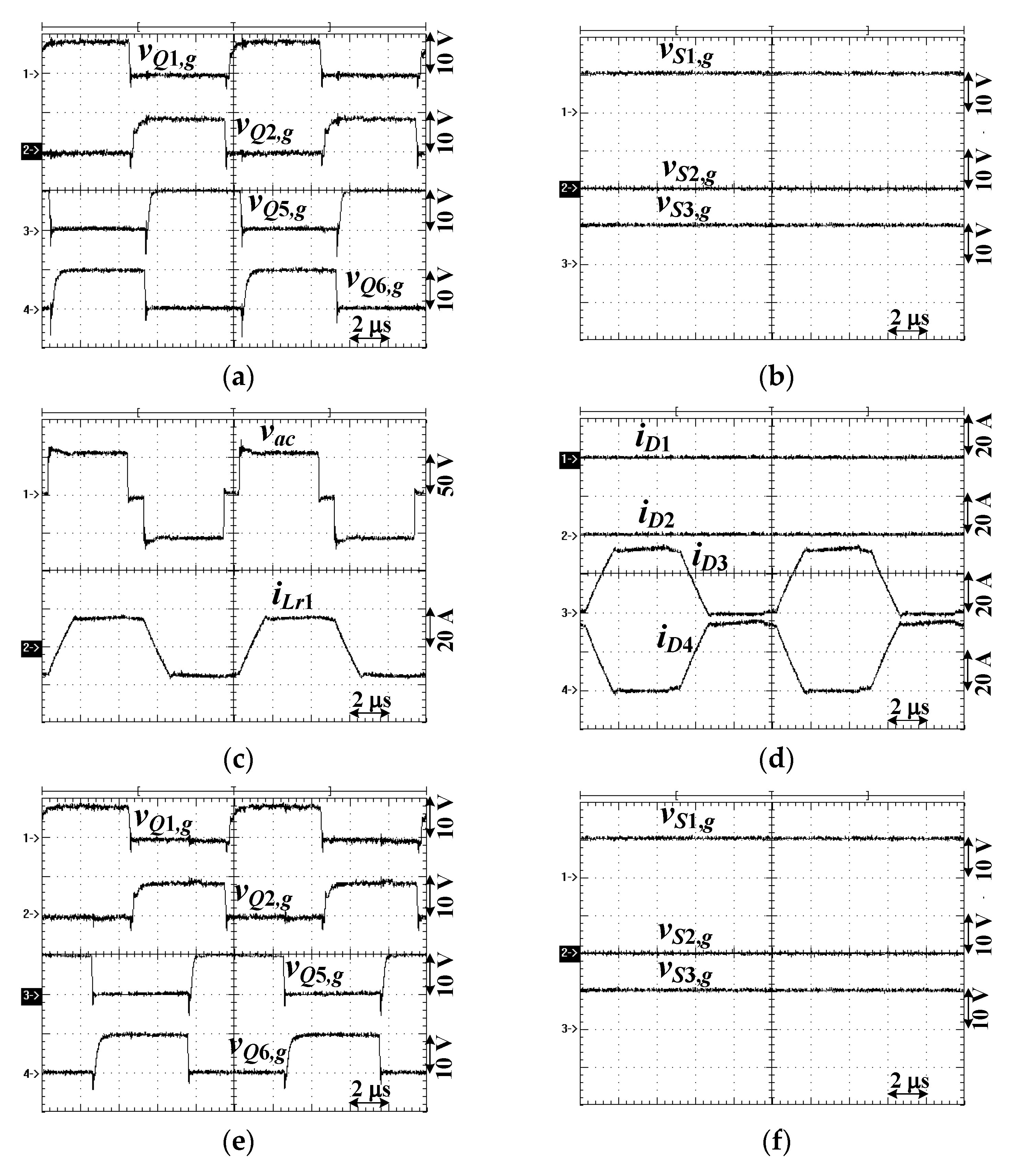
Figure 7.
Measured results under the low voltage range and full load: (a) switch waveforms vQ1,g ~ vQ4,g at Vin = 30 V, (b) AC switch waveforms vS1,g ~ vS3,g at Vin = 30 V, (c) vab and iLr1 at Vin = 30 V, (d) iD1 ~ iD4 at Vin = 30 V, (e) switch waveforms vQ1,g ~ vQ4,g at Vin = 63 V, (f) AC switch waveforms vS1,g ~ vS3,g at Vin = 63 V, (g) vab and iLr1 at Vin = 63 V, and (h) iD1 ~ iD4 at Vin = 63 V.


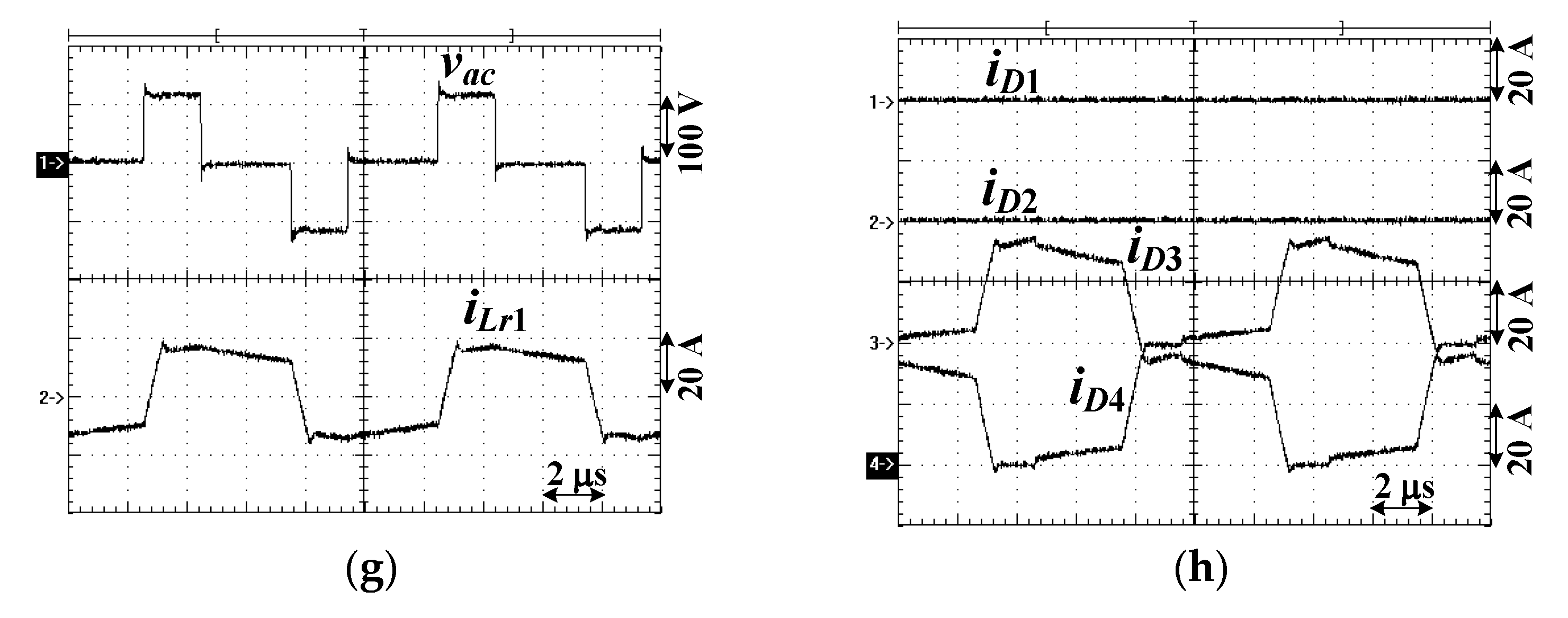
Figure 8.
Experimental waveforms under medium input voltage range and full load: (a) switch waveforms vQ1,g, vQ2,g, vQ5,g, and vQ6,g at Vin = 57 V, (b) AC switch waveforms vS1,g ~ vS3,g at Vin = 57 V, (c) vab and iLr1 at Vin = 57 V, (d) iD1 ~ iD4 at Vin = 57 V, (e) switch waveforms vQ1,g, vQ2,g, vQ5,g, and vQ6,g at Vin = 123 V, (f) AC switch waveforms vS1,g ~ vS3,g at Vin = 123 V, (g) vab and iLr1 at Vin = 123 V, and (h) iD1 ~ iD4 at Vin = 123 V.


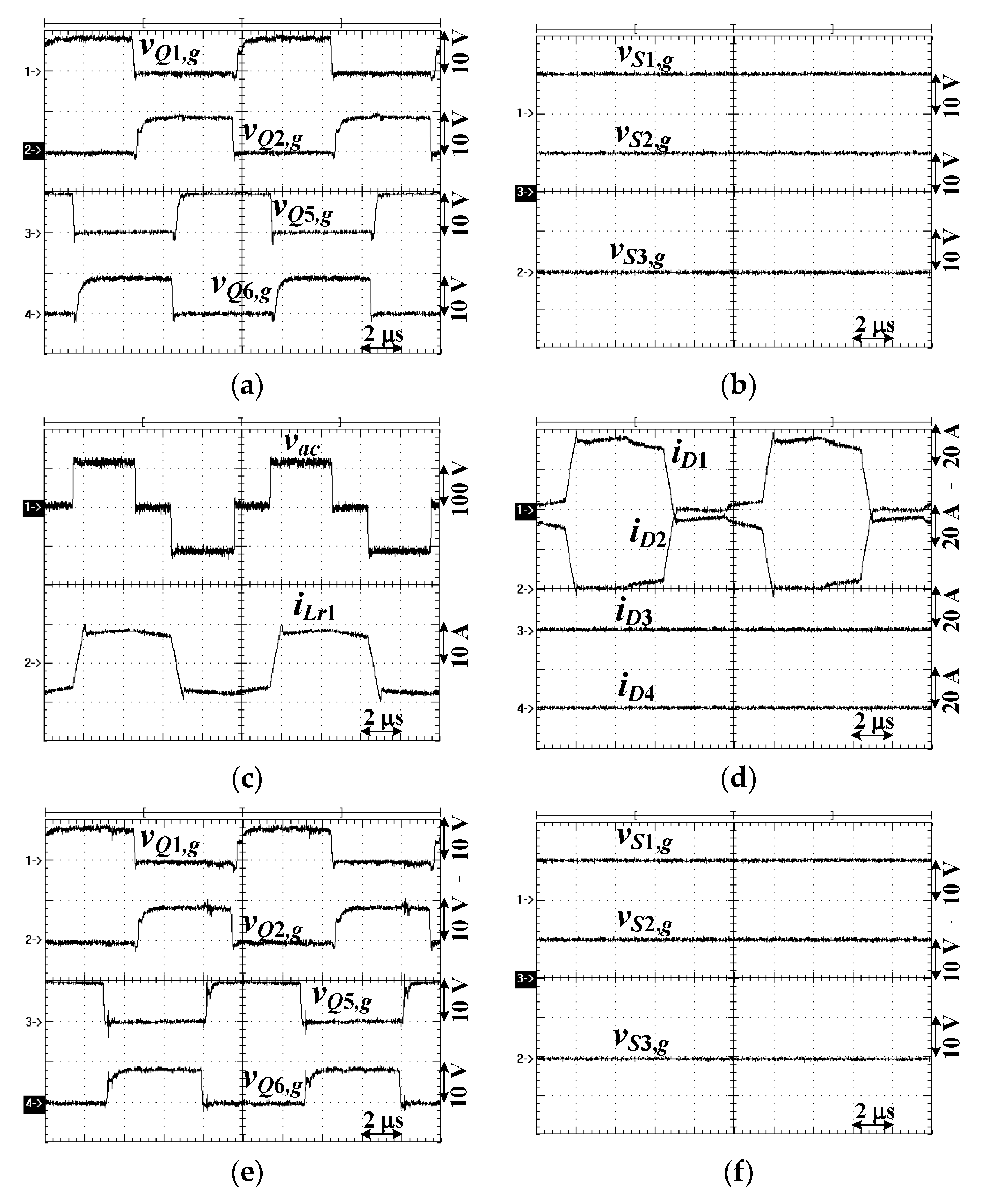
Figure 9.
Experimental waveforms under high input voltage range and full load: (a) switch waveforms vQ1,g, vQ2,g, vQ5,g, and vQ6,g at Vin = 117 V, (b) AC switch waveforms vS1,g ~ vS3,g at Vin = 117 V, (c) vab and iLr1 at Vin = 117 V, (d) iD1 ~ iD4 at Vin = 117 V, (e) switch waveforms vQ1,g, vQ2,g, vQ5,g, and vQ6,g at Vin = 240 V, (f) AC switch waveforms vS1,g ~ vS3,g at Vin = 240 V, (g) vab and iLr1 at Vin = 240 V, and (h) iD1 ~ iD4 at Vin = 240 V.


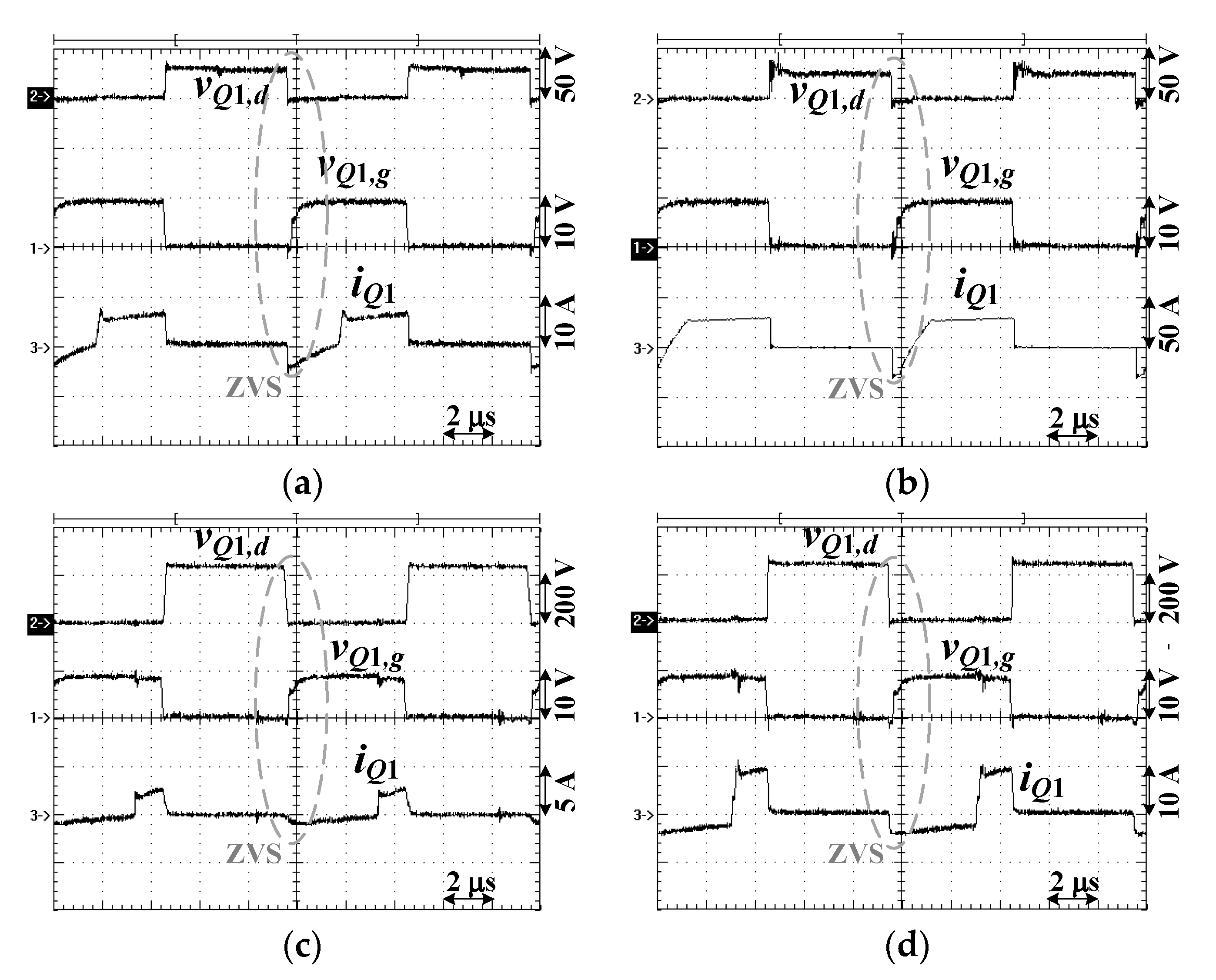
Figure 10.
Experimental waveforms of Q1 at (a) Vin = 30 V and 20% load, (b) Vin = 30 V and 100% load, (c) Vin = 240 V and 20% load, and (d) Vin = 240 V and 100% load.
Figure 10.
Experimental waveforms of Q1 at (a) Vin = 30 V and 20% load, (b) Vin = 30 V and 100% load, (c) Vin = 240 V and 20% load, and (d) Vin = 240 V and 100% load.

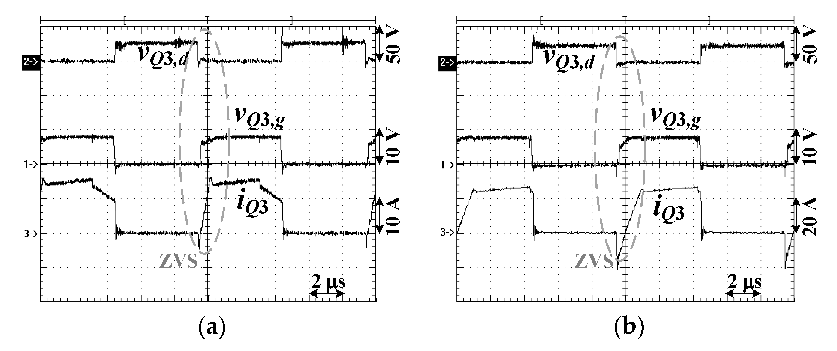
Figure 11.
Experimental waveforms of Q3 at (a) Vin = 30 V and 50% load and (b) Vin = 30 V and 100% load.
Figure 11.
Experimental waveforms of Q3 at (a) Vin = 30 V and 50% load and (b) Vin = 30 V and 100% load.

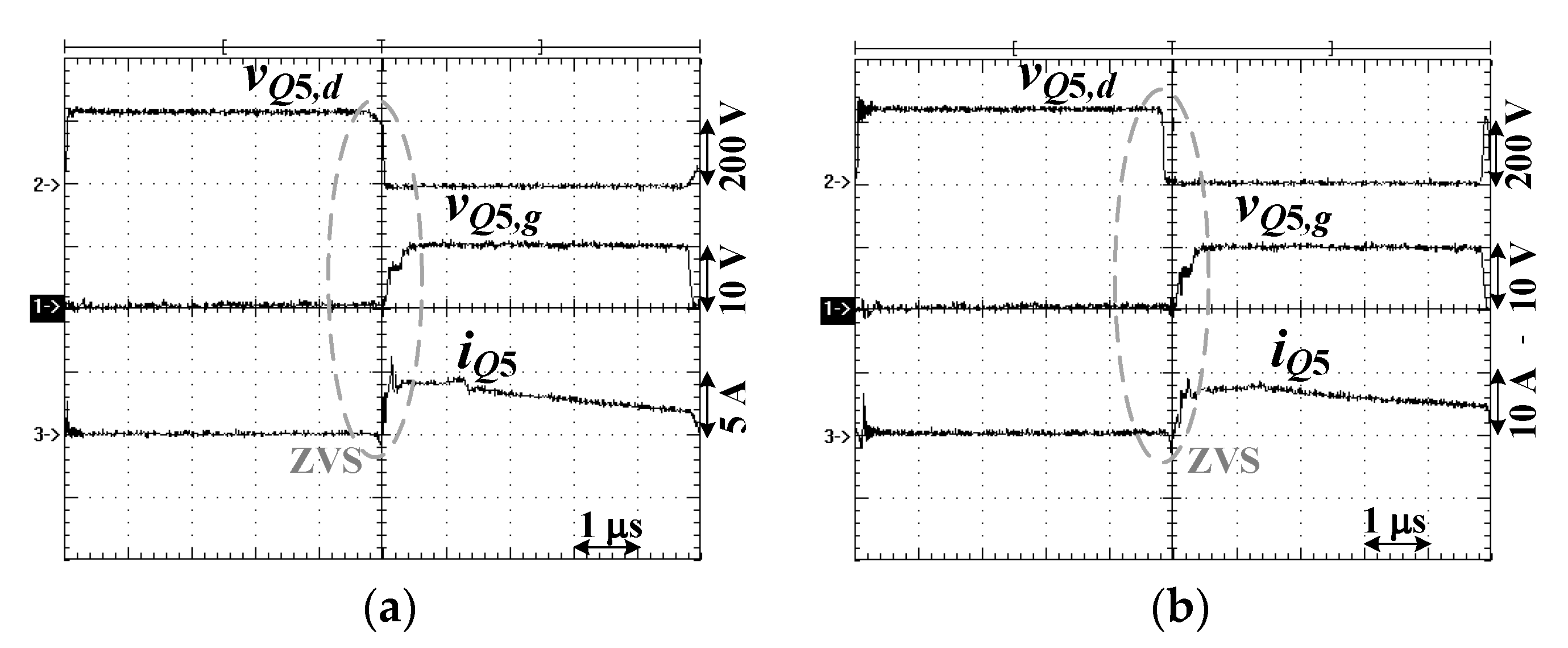
Figure 12.
Experimental waveforms of Q5 at (a) Vin = 240 V and 50% load and (b) Vin = 240 V and 100% load.
Figure 12.
Experimental waveforms of Q5 at (a) Vin = 240 V and 50% load and (b) Vin = 240 V and 100% load.

Figure 13.
Circuit efficiencies under (a) low voltage range (Vin = 30 V ~ 63 V), (b) medium voltage range (Vin = 57 V ~ 123 V), and (c) high voltage range (Vin = 117 V ~ 240 V).
Figure 13.
Circuit efficiencies under (a) low voltage range (Vin = 30 V ~ 63 V), (b) medium voltage range (Vin = 57 V ~ 123 V), and (c) high voltage range (Vin = 117 V ~ 240 V).

Figure 14.
Measured waveforms under full load (a) Vin, vS1,g, vQ3,g, vQ4,g, (b) Vin, vS2,g, and (c) Vin, Vo.
Figure 14.
Measured waveforms under full load (a) Vin, vS1,g, vQ3,g, vQ4,g, (b) Vin, vS2,g, and (c) Vin, Vo.


© 2020 by the authors. Licensee MDPI, Basel, Switzerland. This article is an open access article distributed under the terms and conditions of the Creative Commons Attribution (CC BY) license (http://creativecommons.org/licenses/by/4.0/).
Share and Cite
MDPI and ACS Style
Lin, B.-R.; Chang, J.-W. Analysis and Verification of a Wide Input Voltage PWM Converter with Variable Windings. Energies 2020, 13, 1634. https://doi.org/10.3390/en13071634
AMA Style
Lin B-R, Chang J-W. Analysis and Verification of a Wide Input Voltage PWM Converter with Variable Windings. Energies. 2020; 13(7):1634. https://doi.org/10.3390/en13071634
Chicago/Turabian StyleLin, Bor-Ren, and Ji-Wei Chang. 2020. "Analysis and Verification of a Wide Input Voltage PWM Converter with Variable Windings" Energies 13, no. 7: 1634. https://doi.org/10.3390/en13071634
Note that from the first issue of 2016, this journal uses article numbers instead of page numbers. See further details here.