Practical Considerations for Designing Reliable DC/DC Converters, Applied to a BIPV Case

 , , , , , and
Abstract
:1. Introduction
2. Reliability Criteria for Topology Assessment
2.1. Lowest Component Count
2.2. Transistors and Diodes
2.3. Capacitors
2.4. Inductors and Transformers
2.5. Soft Switching
3. Methods to Further Improve Reliability and Availability
3.1. Redundancy
3.2. Standardized Parts
3.3. Control
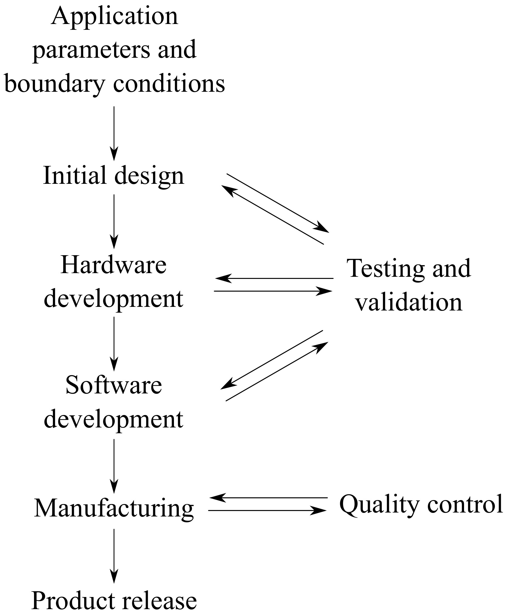
4. Methodology
- Use topologies with a minimal amount of components. Not only the component itself can fail but also the solder joints might crack after severe thermal loading.
- Use topologies with a minimal amount of active switches and avoid replacing passive switches with active ones. Preferably use active switches that do not require a floating power supply as this further increases the component count and circuit complexity.
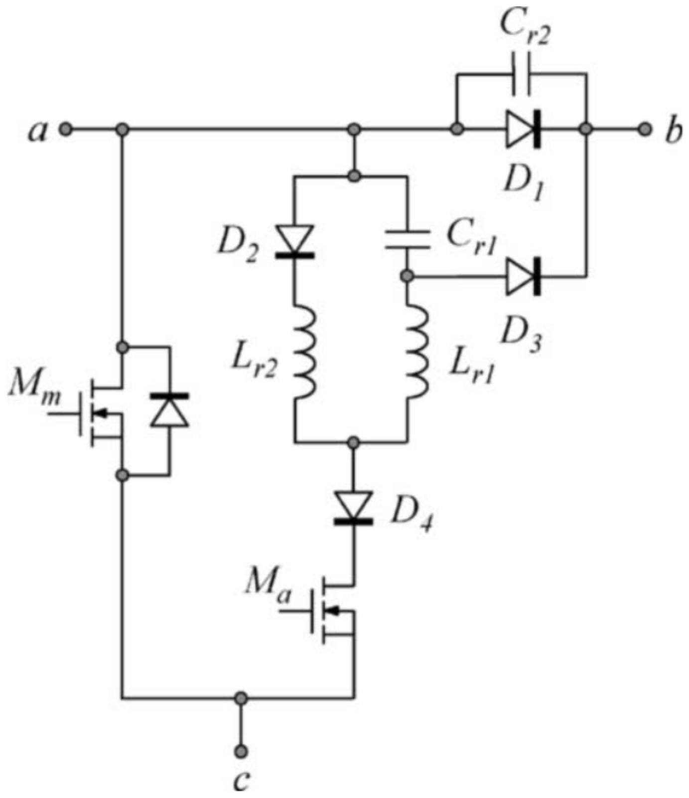
- Avoid the use of topologies with resonant capacitors to allow SS. The high currents that flow through the capacitor will lead to a strong thermal loading. Make preferrably use of the parasitic capacitance of the components, such as the . Also ZVT/ZCT circuits need to be avoided as they strongly increase component count and complexity.
- Avoid to rely on ZVT/ZCT circuits in order to decrease the heat sink size.
- Inductor- or transformer-based topologies are preferred over capacitor-based designs due to their inherent robustness at high temperatures.
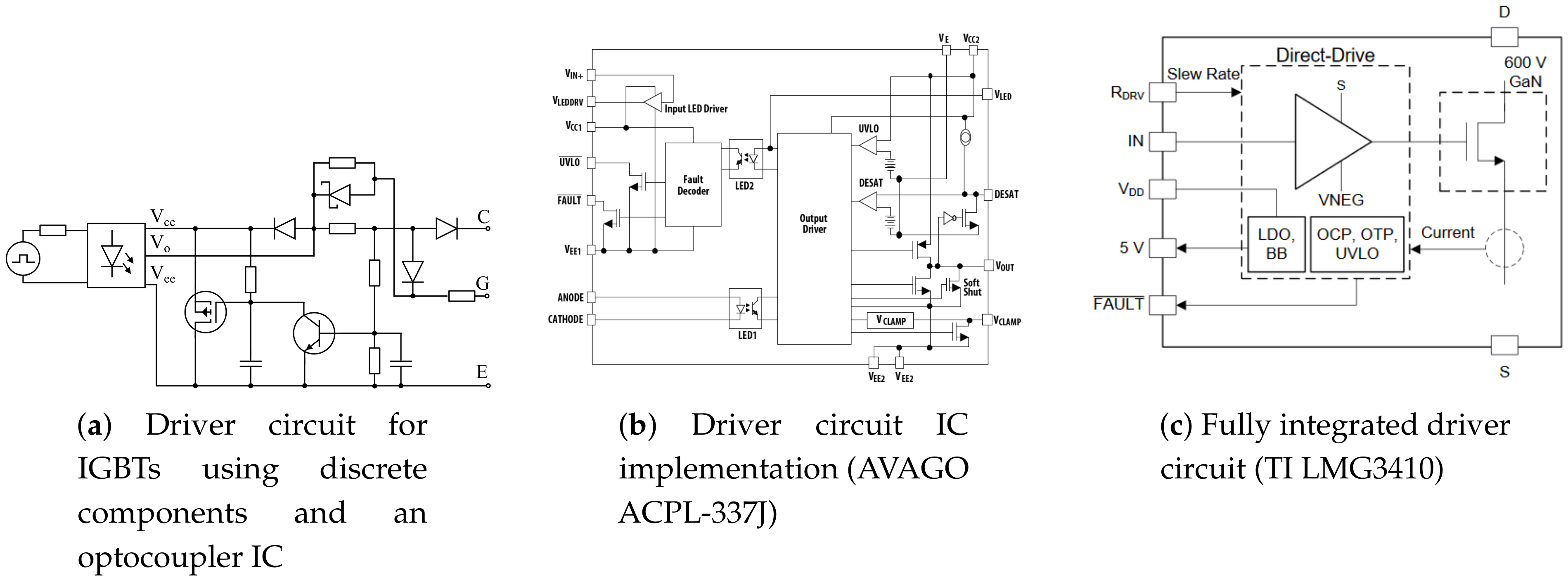
- Choose a gate driver IC that requires a minimum of external components and does not use optical isolation. Consider the combined use of a driver with transistor to further reduce the amount of solder joints and the possibility of design errors.
- Active rectification, where diodes are replaced by transistors, is an interesting means to boost effciency. When evaluating the reliability of both solutions, the extra gate driver, isolated power supply and increased circuit complexity need to be taken into account to make an informed decision.
- Bond wire lift-off due to thermal cycling is one of the major failure mechanisms of transistors. Components exist that employ alternative techniques such as direct copper clip bonding and are preferred in terms of reliability.
- Aluminum electrolytic capacitors need to be avoided in high temperature applications, as the electrolyte evaporates more rapidly, leading to component failure. Alternatives such as MLCCs or film capacitors can be chosen. For MLCCs, preferably components with J-leads, flexible terminations or open mode designs are used to avoid the short-circuit failure mode. For film capacitors, providing sufficient margin on the voltage can further increase their lifetime.
- Inductors and transformers are inherently robust parts from a temperature perspective. Powder cores are preferrably avoided when the component operates continuously above , as thermal aging can lead to increased core losses over time.
- Avoid to rely on ZVT/ZCT circuits in order to decrease the heat sink size. Design the cooling system with sufficient margin such that, in case of malfunctioning of the SS circuit, the junction temperature does not increase beyond the thermal limit as specified in the datasheet.
- Redundancy can strongly increase converter reliability but also raises the price, and possibly the circuit complexity, considerably.
- Make use of parts that have an automotive (AEC-Qxxx) or space (EPPL) certification.
5. Case Study: BIPV
5.1. BIPV as a Mission-Critical Application
5.2. Electrical Requirements
5.3. Initial Design—Converter Topology Selection
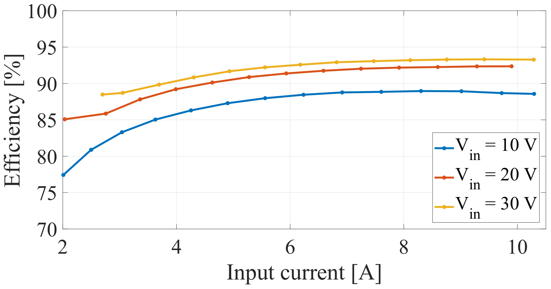
5.4. Hardware Development
6. Conclusions
Author Contributions
Funding
Conflicts of Interest
References
- Chan, F.; Calleja, H. Design Strategy to Optimize the Reliability of Grid-Connected PV Systems. IEEE Trans. Ind. Electron. 2009, 56, 4465–4472. [Google Scholar] [CrossRef]
- Ristow, A.; Begovic, M.; Pregelj, A.; Rohatgi, A. Development of a Methodology for Improving Photovoltaic Inverter Reliability. IEEE Trans. Ind. Electron. 2008, 55, 2581–2592. [Google Scholar] [CrossRef]
- Harb, S.; Balog, R.S. Reliability of Candidate Photovoltaic Module-Integrated-Inverter (PV-MII) Topologies—A Usage Model Approach. IEEE Trans. Power Electron. 2013, 28, 3019–3027. [Google Scholar] [CrossRef]
- Khosroshahi, A.; Abapour, M.; Sabahi, M. Reliability Evaluation of Conventional and Interleaved DC–DC Boost Converters. IEEE Trans. Power Electron. 2015, 30, 5821–5828. [Google Scholar] [CrossRef]
- U.S. Department of Defense. Military Handbook MIL-HDBK-217F, Reliability Prediction of Electronic Equipment; Technical Report; U.S. Department of Defense: Washington, DC, USA, 1995.
- Technologies, T. Special Report SR-332: Reliability Prediction Procedure for Electronic Equipment, Issue 4; Technical Report; Ericsson Inc.: Plano, TX, USA, 2016. [Google Scholar]
- Pandian, G.P.; Das, D.; Li, C.; Zio, E.; Pecht, M. A critique of reliability prediction techniques for avionics applications. Chin. J. Aeronaut. 2018, 31, 10–20. [Google Scholar] [CrossRef]
- Wang, H.; Liserre, M.; Blaabjerg, F.; de Place Rimmen, P.; Jacobsen, J.B.; Kvisgaard, T.; Landkildehus, J. Transitioning to Physics-of-Failure as a Reliability Driver in Power Electronics. IEEE J. Emerg. Sel. Top. Power Electron. 2014, 2, 97–114. [Google Scholar] [CrossRef]
- Ma, K.; Wang, H.; Blaabjerg, F. New Approaches to Reliability Assessment: Using physics-of-failure for prediction and design in power electronics systems. IEEE Power Electron. Mag. 2016, 3, 28–41. [Google Scholar] [CrossRef]
- Pecht, M.; Gu, J. Physics-of-failure-based prognostics for electronic products. Trans. Inst. Meas. Control 2009, 31, 309–322. [Google Scholar] [CrossRef]
- Hung Chung, H.S.; Wang, H.; Blaabjerg, F.; Pecht, M. Reliability of Power Electronic Converter Systems; The Institution of Engineering and Technology: London, UK, 2015. [Google Scholar]
- Sastry, A.; Kulasekaran, S.; Flicker, J.; Ayyanar, R.; TamizhMani, G.; Roy, J.; Srinivasan, D.; Tilford, I. Failure modes and effect analysis of module level power electronics. In Proceedings of the 2015 IEEE 42nd Photovoltaic Specialist Conference (PVSC), New Orleans, LA, USA, 14–19 June 2015; pp. 1–3. [Google Scholar] [CrossRef]
- Gadalla, B.; Schaltz, E.; Blaabjerg, F. A survey on the reliability of power electronics in electro-mobility applications. In Proceedings of the 2015 Intl Aegean Conference on Electrical Machines Power Electronics (ACEMP), 2015 Intl Conference on Optimization of Electrical Electronic Equipment (OPTIM) 2015 Intl Symposium on Advanced Electromechanical Motion Systems (ELECTROMOTION), Side, Turkey, 2–4 September 2015; pp. 304–310. [Google Scholar] [CrossRef]
- Song, Y.; Wang, B. Survey on Reliability of Power Electronic Systems. IEEE Trans. Power Electron. 2013, 28, 591–604. [Google Scholar] [CrossRef]
- Petrone, G.; Spagnuolo, G.; Teodorescu, R.; Veerachary, M.; Vitelli, M. Reliability Issues in Photovoltaic Power Processing Systems. IEEE Trans. Ind. Electron. 2008, 55, 2569–2580. [Google Scholar] [CrossRef]
- Sande, W.V.D.; Ravyts, S.; Sangwongwanich, A.; Manganiello, P.; Yang, Y.; Blaabjerg, F.; Driesen, J.; Daenen, M. A mission profile-based reliability analysis framework for photovoltaic DC-DC converters. Microelectron. Reliab. 2019, 100–101, 113383. [Google Scholar] [CrossRef] [Green Version]
- Ravyts, S.; Dalla Vecchia, M.; Van den Broeck, G.; Driesen, J. Review on Building-Integrated Photovoltaics Electrical System Requirements and Module-Integrated Converter Recommendations. Energies 2019, 12, 1532. [Google Scholar] [CrossRef] [Green Version]
- Ravyts, S.; Vecchia, M.D.; den Broeck, G.V.; Yordanov, G.H.; Gonçalves, J.E.; Moschner, J.D.; Saelens, D.; Driesen, J. Embedded BIPV module-level DC/DC converters: Classification of optimal ratings. Renew. Energy 2020, 146, 880–889. [Google Scholar] [CrossRef]
- Chen, G.; Burgos, R.; Liang, Z.; Lacaux, F.; Wang, F.; van Wyk, J.D.; Odendaal, W.G.; Boroyevich, D. Reliability-oriented design considerations for high-power converter modules. In Proceedings of the 2004 IEEE 35th Annual Power Electronics Specialists Conference (IEEE Cat. No.04CH37551), Aachen, Germany, 20–25 June 2004; Volume 1, pp. 419–425. [Google Scholar] [CrossRef]
- Bajenesco, T. CTR degradation and ageing problem of optocouplers. In Proceedings of the 4th International Conference on Solid-State and IC Technology, Beijing, China, 24–28 October 1995; pp. 173–175. [Google Scholar] [CrossRef]
- Wu, H.; He, S.; Chen, X.; Xu, G.; Lei, D. Failure mechanisms and package reliability issues in optocouplers. In Proceedings of the 2016 17th International Conference on Electronic Packaging Technology (ICEPT), Wuhan, China, 16–19 August 2016; pp. 1240–1243. [Google Scholar] [CrossRef]
- Shi, Z.; Lu, Y.; Chen, Y.; Feng, J. The real-time fault diagnosis of optocoupler in switching mode power supply. In Proceedings of the 2014 10th International Conference on Reliability, Maintainability and Safety (ICRMS), Guangzhou, China, 6–8 August 2014; pp. 263–266. [Google Scholar] [CrossRef]
- Analog Devices. Isolated Precision Half-Bridge Driver; Analog Devices: Norwood, MA, USA, 2017. [Google Scholar]
- Kittappa, M. Replace Your Aging Optocoupler Gate Driver. 2019. Available online: https://e2e.ti.com/blogs_/b/powerhouse/archive/2019/03/14/replace-your-aging-optocoupler-gate-driver (accessed on 14 February 2020).
- Texas Instruments. Opto-Compatible Single-Channel Isolated Gate Driver. October 2018. Rev. October 2019. Available online: http://www.ti.com/lit/ds/symlink/ucc23513.pdf (accessed on 14 January 2020).
- Graditi, G.; Adinolfi, G.; Femia, N.; Vitelli, M. Comparative analysis of Synchronous Rectification Boost and Diode Rectification Boost converter for DMPPT applications. In Proceedings of the 2011 IEEE International Symposium on Industrial Electronics, Gdansk, Poland, 27–30 June 2011; pp. 1000–1005. [Google Scholar] [CrossRef]
- Yang, S.; Bryant, A.; Mawby, P.; Xiang, D.; Ran, L.; Tavner, P. An Industry-Based Survey of Reliability in Power Electronic Converters. IEEE Trans. Ind. Appl. 2011, 47, 1441–1451. [Google Scholar] [CrossRef]
- Wang, H.; Liserre, M.; Blaabjerg, F. Toward Reliable Power Electronics: Challenges, Design Tools, and Opportunities. IEEE Ind. Electron. Mag. 2013, 7, 17–26. [Google Scholar] [CrossRef] [Green Version]
- Smet, V.; Forest, F.; Huselstein, J.; Richardeau, F.; Khatir, Z.; Lefebvre, S.; Berkani, M. Ageing and Failure Modes of IGBT Modules in High-Temperature Power Cycling. IEEE Trans. Ind. Electron. 2011, 58, 4931–4941. [Google Scholar] [CrossRef]
- Eckert, T.; Muller, W.H.; Nissen, N.F.; Reichl, H. A solder joint fatigue life Model for combined vibration and temperature environments. In Proceedings of the Electronic Components and Technology Conference, San Diego, CA, USA, 26–29 May 2009; pp. 522–528. [Google Scholar] [CrossRef]
- Darveaux, R.; Banerji, K. Constitutive Relations for Tin-Based Solder Joints. IEEE Trans. Compon. Hybrids Manuf. Technol. 1992, 1013–1024. [Google Scholar] [CrossRef]
- Norris, K.C.; Landzberg, A.H. Reliability of Controlled Collapse Interconnections. IBM J. Res. Dev. 1986, 13, 266–271. [Google Scholar] [CrossRef]
- Musallam, M.; Yin, C.; Bailey, C.; Johnson, M. Mission Profile-Based Reliability Design and Real-Time Life Consumption Estimation in Power Electronics. IEEE Trans. Power Electron. 2015, 30, 2601–2613. [Google Scholar] [CrossRef] [Green Version]
- Van De Sande, W.; Spiliotis, K.; Gonçalves, J.; Ravyts, S.; Driesen, J.; Saelens, D.; Daenen, M. Reliability comparison of a DC-DC converter placed in Building-Integrated Photovoltaic module frames. In Proceedings of the International Conference on Renewable Energy Research and Applications (ICRERA), Paris, France, 14–17 October 2018; pp. 1–5. [Google Scholar]
- Lwin, K.K.; Tubillo, C.E.; Dimaano Panumard, T.J.; Suthiwongsunthorn, N.; Sirinorakul, S. Copper clip package for high performance MOSFETs and its optimization. In Proceedings of the 2016 IEEE 18th Electronics Packaging Technology Conference (EPTC), Singapore, 30 November–3 December 2016; pp. 123–128. [Google Scholar] [CrossRef]
- Woo, D.R.M.; Yuan, H.H.; Li, J.A.J.; Bum, L.J.; Hengyun, Z. Miniaturized Double Side Cooling Packaging for High Power 3 Phase SiC Inverter Module with Junction Temperature over 220 °C. In Proceedings of the 2016 IEEE 66th Electronic Components and Technology Conference (ECTC), Las Vegas, NV, USA, 31 May–3 June 2016; pp. 1190–1196. [Google Scholar] [CrossRef]
- Kumar Prasobhu, P.; Raveendran, V.; Buticchi, G.; Liserre, M. Active Thermal Control of GaN-Based DC/DC Converter. IEEE Trans. Ind. Appl. 2018, 54, 3529–3540. [Google Scholar] [CrossRef]
- Landrock, C.K.; Kaminska, B. High temperature polymer capacitors for aerospace applications. In Proceedings of the 2010 Design, Automation Test in Europe Conference Exhibition (DATE 2010), Dresden, Germany, 8–12 March 2010; pp. 1349–1352. [Google Scholar] [CrossRef]
- Wang, H.; Blaabjerg, F. Reliability of Capacitors for DC-Link Applications in Power Electronic Converters—An Overview. IEEE Trans. Ind. Appl. 2014, 50, 3569–3578. [Google Scholar] [CrossRef] [Green Version]
- Gupta, A.; Yadav, O.P.; DeVoto, D.J.; Major, J. A Review of Degradation Behavior and Modeling of Capacitors. In Proceedings of the 2018 International Technical Conference and Exhibition on Packaging and Integration of Electronic and Photonic Microsystems (InterPACK 2018), San Francisco, CA, USA, 28–30 August 2018. [Google Scholar] [CrossRef] [Green Version]
- Shrivastava, A.; Azarian, M.H.; Pecht, M. Failure of Polymer Aluminum Electrolytic Capacitors Under Elevated Temperature Humidity Environments. IEEE Trans. Compon. Packag. Manuf. Technol. 2017, 7, 745–750. [Google Scholar] [CrossRef]
- Macomber, L.L.; Cornell Dubilier, L.; Carolina, S. Solid Polymer Aluminum Capacitor Chips in DC-DC Converter Modules Reduce Cost and Size and Improve High-Frequency Performance. In Proceedings of the PCIM Power Electronics 2001 Proceeding for the Power Systems World Conference, Rosemont, IL, USA, 11–13 September 2001. [Google Scholar]
- Y. Freeman, P.L. High Temperature—High Voltage Solid Electrolytic Tantalum Capacitors. In Proceedings of the IMAPS High Temperature Electronics Network (HiTEN 2019), Oxford, UK, 8–10 July 2019; pp. 1–8. [Google Scholar] [CrossRef]
- Snyder, H.L. A 300 °C High Reliability HALT/HAST Screening/Sorting Procedure for Ceramic Capacitors. Addit. Pap. Present 2018, 2018, 000129–000137. [Google Scholar] [CrossRef]
- Liu, D.D.; Sampson, M.J. Reliability evaluation of base-metal-electrode multilayer ceramic capacitors for potential space applications. In Proceedings of the CARTS 2011 Conference Proceedings, Greenbelt, MD, USA, 28–31 March 2011. [Google Scholar]
- John, M.; Frank, H.; Michael, C. A Technical Evaluation of Surface Mount Base Metal Capacitors (BME) X7R for the European Space Agency. Technical Report. 2011. Available online: https://www.google.com/url?sa=t&rct=j&q=&esrc=s&source=web&cd=1&cad=rja&uact=8&ved=2ahUKEwiA5KarzNDnAhUBy6QKHchqB8sQFjAAegQIBBAB&url=https (accessed on 14 January 2020).
- Franklin, J.; Bultitude, J.; McConnell, J.; Phillips, R.; Laps, M.; John, P.; Ashburn, T. High capacitance stacked multi-layer ceramic capacitors for power supplies. In Proceedings of the CARTS 2010 Conference Proceedings, New Orleans, LA, USA, 15–18 March 2010. [Google Scholar]
- Stewart, M. A soft termination MLCC solution to guard against capacitor crack failures. In Proceedings of the 25th Symposium for Passive Components, CARTS, Palm Springs, CA, USA, 21–24 March 2005; Volume 5, pp. 219–224. [Google Scholar]
- Hopwood, S. Multilayer Ceramic Capacitors in Automotive. Power Electron. Mag. 2017, 2, 36–38. [Google Scholar]
- Menzel, S. ABC of Capacitors: Basic Principles, Characteristics and Capacitor Types; Wurth Elektronik: Niedernhall, Germany, 2014. [Google Scholar]
- MLCC C0G Guide for Resonant Circuit. Available online: https://product.tdk.com/info/en/products/capacitor/ceramic/mlcc/technote/solution/mlcc04/index.html (accessed on 14 January 2020).
- Xu, J.; Gu, L.; Hernandez, E.; Rivas-Davila, J. Effect of Class 2 Ceramic Capacitance Variations on Switched Capacitor and Resonant Switched Capacitor Converters. In Proceedings of the 2018 IEEE 19th Workshop on Control and Modeling for Power Electronics (COMPEL), Padua, Italy, 25–28 June 2018; pp. 1–7. [Google Scholar] [CrossRef]
- Qin, S.; Ma, S.; Boggs, S.A. The mechanism of clearing in metalized film capacitors. In Proceedings of the 2012 IEEE International Symposium on Electrical Insulation, San Juan, PR, USA, 10–13 June 2012; pp. 592–595. [Google Scholar] [CrossRef]
- Cavallini, A.; Fabiani, D.; Mazzanti, G.; Montanari, G.C. Models for degradation of self-healing capacitors operating under voltage distortion and temperature. In Proceedings of the 6th International Conference on Properties and Applications of Dielectric Materials (Cat. No.00CH36347), Xi’an, China, 21–26 June 2000; Volume 1, pp. 108–111. [Google Scholar] [CrossRef]
- Roy, J.; Ayyanar, R. GaN based high gain non-isolated DC-DC stage of microinverter with extended-duty-ratio boost. In Proceedings of the 2016 IEEE Energy Conversion Congress and Exposition (ECCE), Milwaukee, WI, USA, 18–22 September 2016. [Google Scholar] [CrossRef]
- Chatterjee, U.; Gelagaev, R.; Masolin, A.; Driesen, J. Design of an intra-module DC-DC converter for PV application: Design considerations and prototype. In Proceedings of the IECON 2014—40th Annual Conference of the IEEE Industrial Electronics Society, Dallas, TX, USA, 29 October–1 November 2014; pp. 2017–2022. [Google Scholar] [CrossRef]
- Oni, B.; Griffin, T.; Cunningham, K.; Kapustka, B.; Luna, S. Characterizing Space-Flight Inductors and Transformer Failures; NASA IEE Links. 2002, Volume 8. Available online: https://www.google.com/url?sa=t&rct=j&q=&esrc=s&source=web&cd=1&cad=rja&uact=8&ved=2ahUKEwjByLiF0NDnAhVD26QKHR5nCpAQFjAAegQIAxAB&url=https (accessed on 14 February 2020).
- Tremlett, P.; Elliot, P.; Tena, P. Origami for Tight Spaces—3D 250C PCB Assemblies for Control Systems. In Additional Conferences (Device Packaging, HiTEC, HiTEN, & CICMT); International Microelectronics Assembly and Packaging Society: Durham, NC, USA, 2019; Volume 2019, pp. 000034–000038. [Google Scholar] [CrossRef]
- Inc., M. Designing with Magnetic Cores at High Temperatures. In Proceedings of the PCIM 2001 Europe Official Proc. of 43rd International Power Electronics Conference, Nurnberg, Germany, 7–9 June 2005. [Google Scholar]
- Magnetics, V. Using IHLP’s in Automotive Applications; Technical Report; Vishay Dale. 2008. Available online: https://www.vishay.com/docs/34256/ihlpaapp.pdf (accessed on 14 February 2020).
- Ferreira Costa, L.; Liserre, M. Failure Analysis of the dc-dc Converter: A Comprehensive Survey of Faults and Solutions for Improving Reliability. IEEE Power Electron. Mag. 2018, 5, 42–51. [Google Scholar] [CrossRef]
- Wang, C.M. Novel zero-Voltage-transition PWM DC-DC converters. IEEE Trans. Ind. Electron. 2006, 53, 254–262. [Google Scholar] [CrossRef]
- Gradinger, T.; Agostini, F.; Cottet, D. Two-Phase Cooling of Hot-Swappable Modular Converters. In Proceedings of the PCIM Europe 2014; International Exhibition and Conference for Power Electronics, Intelligent Motion, Renewable Energy and Energy Management, Nuremberg, Germany, 20–22 May 2014; pp. 1–8. [Google Scholar]
- Aghdam, F.H.; Abapour, M. Reliability and Cost Analysis of Multistage Boost Converters Connected to PV Panels. IEEE J. Photovolt. 2016, 6, 981–989. [Google Scholar] [CrossRef]
- Gallina, G. The European Preferred Parts List. Esa Sp 2002, 507, 287–289. [Google Scholar]
- Andresen, M.; Ma, K.; Buticchi, G.; Falck, J.; Blaabjerg, F.; Liserre, M. Junction Temperature Control for More Reliable Power Electronics. IEEE Trans. Power Electron. 2018, 33, 765–776. [Google Scholar] [CrossRef] [Green Version]
- Forouzesh, M.; Siwakoti, Y.P.; Gorji, S.A.; Blaabjerg, F.; Lehman, B. Step-Up DC–DC Converters: A Comprehensive Review of Voltage-Boosting Techniques, Topologies, and Applications. IEEE Trans. Power Electron. 2017, 32, 9143–9178. [Google Scholar] [CrossRef]
- Vecchia, M.D.; Van den Broeck, G.; Ravyts, S.; Tant, J.; Driesen, J. Modified step-down series-capacitor buck converter with insertion of a Valley-Fill structure. IET Power Electron. 2019, 12, 3306–3314. [Google Scholar] [CrossRef]
- Dalla Vecchia, M.; Lazzarin, T.B. Hybrid DC-DC buck converter with active switched capacitor cell and low voltage gain. In Proceedings of the 2016 IEEE Energy Conversion Congress and Exposition (ECCE), Milwaukee, WI, USA, 18–22 September 2016; pp. 1–6. [Google Scholar] [CrossRef]
- Vecchia, M.D.; Salvador, M.A.; Lazzarin, T.B. Hybrid Nonisolated DC–DC Converters Derived From a Passive Switched-Capacitor Cell. IEEE Trans. Power Electron. 2018, 33, 3157–3168. [Google Scholar] [CrossRef]
- Liao, Z.; Lei, Y.; Pilawa-Podgurski, R.C.N. Analysis and Design of a High Power Density Flying-Capacitor Multilevel Boost Converter for High Step-Up Conversion. IEEE Trans. Power Electron. 2019, 34, 4087–4099. [Google Scholar] [CrossRef]
- Dal Pont, N.C.; Dalla Vecchia, M.; Waltrich, G.; Lazzarin, T.B. Step-up inverter conceived by the integration between a Full-Bridge inverter and a Switched Capacitor Converter. In Proceedings of the 2015 IEEE 13th Brazilian Power Electronics Conference and 1st Southern Power Electronics Conference (COBEP/SPEC), Fortaleza, Brazil, 29 November–2 December 2015; pp. 1–6. [Google Scholar] [CrossRef]
- Torrico-Bascopé, G.V. Five-Level PV Inverter Based on a Multi-State Switching Cell. US Patent 9,680,395, 13 June 2017. [Google Scholar]
- Madhukar Rao, A.; Sahoo, M.; Sivakumar, K. A three phase five-level inverter with fault tolerant and energy balancing capability for photovoltaic applications. In Proceedings of the 2016 IEEE International Conference on Power Electronics, Drives and Energy Systems (PEDES), Trivandrum, India, 14–17 December 2016; pp. 1–5. [Google Scholar] [CrossRef]
- Zhang, Z.; Jiang, M.; Yao, Y.; Kang, L. Transformerless three-phase T-type three-level inverter for medium-power photovoltaic systems. In Proceedings of the 2016 IEEE 8th International Power Electronics and Motion Control Conference (IPEMC-ECCE Asia), Hefei, China, 22–26 May 2016; pp. 1592–1595. [Google Scholar] [CrossRef]
- Chacko, R.; Beevi, S.S. Improved DTC using three-level inverter topology for wind power applications. In Proceedings of the 2013 Annual IEEE India Conference (INDICON), Mumbai, India, 13–15 December 2013; pp. 1–5. [Google Scholar] [CrossRef] [Green Version]
- Wang, H.; Ma, K.; Blaabjerg, F. Design for Reliability of Power Electronic Systems. In Proceedings of the IECON 2012—38th Annual Conference on IEEE Industrial Electronics Society, Montreal, QC, Canada, 25–28 October 2012; pp. 33–44. [Google Scholar] [CrossRef]
- ZVEI. Handbook for Robustness Validation of Automotive Electrical/Electronic Modules; Technical Report; ZVEI: Frankfurt am Main, Germany, 2008. [Google Scholar]
- Wang, Y.H.; Liu, W.C.; Kuo, T.H. A 200W MPPT boost converter for BIPV applications with integrated controller. In Proceedings of the 2014 International Symposium on Computer, Consumer and Control, Taichung, Taiwan, 10–12 June 2014; pp. 288–291. [Google Scholar] [CrossRef]
- Das, M.; Agarwal, V. Design and Analysis of a High-Efficiency DC-DC Converter with Soft Switching Capability for Renewable Energy Applications Requiring High Voltage Gain. IEEE Trans. Ind. Electron. 2016, 63, 2936–2944. [Google Scholar] [CrossRef]
- Kasper, M.; Ritz, M.; Bortis, D.; Kolar, J.W. PV Panel-Integrated High Step-up High Efficiency Isolated GaN DC-DC Boost Converter. In Proceedings of the Intelec 2013 35th International Telecommunications Energy Conference, SMART POWER AND EFFICIENCY, Hamburg, Germany, 13–17 October 2013; pp. 1–7. [Google Scholar]
- Ravyts, S.; Vecchia, M.D.; Zwysen, J.; Van den Broeck, G.; Driesen, J. Study on a cascaded DC-DC converter for use in building-integrated photovoltaics. In Proceedings of the 2018 IEEE Texas Power and Energy Conference (TPEC), College Station, TX, USA, 8–9 February 2018; pp. 1–6. [Google Scholar] [CrossRef]
- Ravyts, S.; Dalla Vecchia, M.; Zwysen, J.; van den Broeck, G.; Driesen, J. Comparison between an Interleaved Boost Converter Using Si MOSFETs Versus GaN HEMTs. In Proceedings of the PCIM Europe 2018; International Exhibition and Conference for Power Electronics, Intelligent Motion, Renewable Energy and Energy Management, Nuremberg, Germany, 5–7 June 2018; pp. 1–8. [Google Scholar]
- Ravyts, S.; Vecchia, M.D.; Van den Broeck, G.; Driesen, J. Experimental Comparison of the Efficiency, Power Density and Thermal Performance of Two BIPV Converter Prototypes. In Proceedings of the 2018 IEEE 6th Workshop on Wide Bandgap Power Devices and Applications (WiPDA), Atlanta, GA, USA, 31 October–2 November 2018; pp. 7–13. [Google Scholar] [CrossRef]
- Martinez, W.; Cortes, C.; Yamamoto, M.; Imaoka, J. Effect of inductor parasitic resistances on the voltage gain of high step-up DC–DC converters for electric vehicle applications. IET Power Electron. 2018, 11, 1628–1639. [Google Scholar] [CrossRef]
- Kim, Y.H.; Shin, S.C.; Lee, J.H.; Jung, Y.C.; Won, C.Y. Soft-switching current-fed push-pull converter for 250-W AC module applications. IEEE Trans. Power Electron. 2014, 29, 863–872. [Google Scholar] [CrossRef]
- Liu, B.; Duan, S.; Cai, T. Photovoltaic DC-Building-Module-Based BIPV System—Concept and Design Considerations. Power Electron. IEEE Trans. 2011, 26, 1418–1429. [Google Scholar] [CrossRef]
- Wolfs, P.J. A Current-Sourced DC-DC Converter Derived via the Duality Principle from the Half-Bridge Converter. IEEE Trans. Ind. Electron. 1993, 40, 139–144. [Google Scholar] [CrossRef]
- Erickson, R.W.; Maksimovic, D. Fundamentals of Power Electronics, 2nd ed.; Springer: Berlin, Germany, 2001. [Google Scholar]
- Pevere, A.; Chatterjee, U.; Driesen, J. Current controller modeling for an interleaved boost with voltage multiplier cells for PV applications. In Proceedings of the 2016 IEEE Applied Power Electronics Conference and Exposition (APEC), Long Beach, CA, USA, 20–24 March 2016; pp. 1183–1190. [Google Scholar] [CrossRef]


| Ref. | Topology | Ideal Gain | Input Voltage [V] | Output Voltage [V] | Output Power [W] | Galvanic Isolation | #S | #D | #C | #L |
|---|---|---|---|---|---|---|---|---|---|---|
| [79] | Boost | 12-36 | 48 | 200 | No | 1 | 1 | 2 | 1 | |
| [56] | Boost with VMC | 10-25 | 120 | 200 | No | 2 | 6 | 6 | 2 | |
| [55] | 3-L EDR boost | 20-40 | 225 | 250 | No | 3 | 3 | 4 | 3 | |
| [80] | Passive clamp, coupled inductor boost | 25-50 | 400 | 400 | No | 1 | 3 | 4 | 2 | |
| [81] | Synchronous boost, SR FB | 15-45 | 400 | 275 | Yes | 6 | 2 | 5 | 2 | |
| [82,83,84] | Interleaved boost, SR FB | 10-40 | 400 | 300 | Yes | 7 | 7 | 4 | 4 | |
| [85] | IBIWCI | 7.2-110 | 80-140 | 100 | No | 2 | 4 | 2 | 1 | |
| [86] | Current-Fed Push-Pull | 20-50 | 400 | 250 | Yes | 2 | 2 | 4 | 1 | |
| [87,88] | IIBC | 20-50 | 200 | 200 | Yes | 2 | 4 | 2 | 2 |
| Component | Type | Value |
|---|---|---|
| KEMET C475M1R2C7186 | 100 V, 5 × 4.7 F | |
| BOURNS SRP2313AA-470M | 14 A, 47 H | |
| TOSHIBA TPH3R70APL | 100 V, = 3.1 m | |
| ST STTH12R06 | 600 V, = 1.4 V | |
| EPCOS B32672P5105K000 | 520 V, 4 × 1 F | |
| Payton custom design | n = 5 |
© 2020 by the authors. Licensee MDPI, Basel, Switzerland. This article is an open access article distributed under the terms and conditions of the Creative Commons Attribution (CC BY) license (http://creativecommons.org/licenses/by/4.0/).
Share and Cite
Ravyts, S.; Van De Sande, W.; Vecchia, M.D.; Broeck, G.V.d.; Duraij, M.; Martinez, W.; Daenen, M.; Driesen, J. Practical Considerations for Designing Reliable DC/DC Converters, Applied to a BIPV Case. Energies 2020, 13, 834. https://doi.org/10.3390/en13040834
Ravyts S, Van De Sande W, Vecchia MD, Broeck GVd, Duraij M, Martinez W, Daenen M, Driesen J. Practical Considerations for Designing Reliable DC/DC Converters, Applied to a BIPV Case. Energies. 2020; 13(4):834. https://doi.org/10.3390/en13040834
Chicago/Turabian StyleRavyts, Simon, Wieland Van De Sande, Mauricio Dalla Vecchia, Giel Van den Broeck, Martijn Duraij, Wilmar Martinez, Michael Daenen, and Johan Driesen. 2020. "Practical Considerations for Designing Reliable DC/DC Converters, Applied to a BIPV Case" Energies 13, no. 4: 834. https://doi.org/10.3390/en13040834