Voltage-Balancing Strategy for Three-Level Neutral Point Clamped Cascade Converter under Sequence Pulse Modulation

1
School of Electrical Engineering Southwest Jiaotong University Chengdu, Chengdu 610000, China
2
Aviation Engineering Institute, Civil Aviation Flight University Chengdu, Chengdu 618307, China
*
Author to whom correspondence should be addressed.
Energies 2019, 12(20), 3829; https://doi.org/10.3390/en12203829
Submission received: 29 August 2019
/
Revised: 30 September 2019
/
Accepted: 3 October 2019
/
Published: 10 October 2019
(This article belongs to the Special Issue Function Design and Control of Multilevel Converters)
Abstract
:In response to the unbalanced DC-port fault of three-level neutral point clamped cascaded converter (3LNPC-CC), a sequence pulse modulation (SPM) voltage-balancing strategy is proposed in this paper to balance DC-link voltage, not only within the module but also among modules. With the steps of carrier cascaded calculation and sequence pulse generator, the voltage level of cascaded modules would take a smooth transition. Then the limitation of the SPM strategy is calculated according to the law of volt-second balance and the law of energy conservation. The proposed strategy has the advantage of simple calculation and control stability. Simulation and experimental results show the superiority of the proposed strategy.
1. Introduction
With the increase of voltage and capacity demand, various multilevel topologies are proposed, such as three-level neutral point clamped converter (3LNPC), cascaded H-bridge converter (CHB) and modular multilevel converter (MMC). CHB has been applied in the Power Electronic Traction Transformer (PETT) for the 15 kV single-phase voltage traction system in Europe. Compared with CHB, a three-level neutral point clamped cascaded converter (3LNPC-CC) has larger capacity, lower voltage stress and better harmonics with the same number of modules [1,2,3,4,5,6,7,8,9].
Due to its own structure, the control strategy of 3LNPC-CC aims to power balance, capacitor voltage-balancing, and low harmonics. In the 3LNPC-CC system, the same Alternating current (AC)-link current flows through each converter module. Therefore, the DC-link voltage of each module will determine the active and reactive power distribution [5,6,7,8]. The control and modulation strategy has been an interesting issue to solve problems of the unbalanced voltage.
References [9,10,11,12] propose an auxiliary voltage-balancing circuit to solve the unbalanced problem of capacitor voltage inner the module. However, using extra inductor or capacitor may lead to high cost and low efficiency, although it has a great influence on voltage-balancing within the module. In Reference [4], a strategy is proposed by using redundant vectors to change the current flow direction. This modulation changes switch states inner the module and maintains the output voltage constant, which has been widely used in 3LNPC convertors.
Meanwhile, the unbalanced DC-link voltage is another problem, which may lead to power loss, high harmonics, high cost, and low stability. The mechanism of unbalance DC-link voltage in 3LNPC-CC is caused by the unequal power transmission of each module. There are mainly four categories that may cause the unbalanced DC-link voltage: neutral point clamped cascaded converter (NPC-CC) working as rectifier, battery DC power supply, modulation, and DC-port open-circuit fault [4,5,6,7,8,9,10,11,12,13,14,15,16,17,18,19,20,21,22,23,24,25,26]. Among them, DC-port fault will cause the most serious voltage unbalance, as the power flow of the fault module comes to zero once the DC-link has no input. Therefore, it is necessary to research the voltage-balancing strategy when the DC-port develops an open-circuit fault.
Therefore, researches on voltage-balancing of the cascaded converter are mainly focused on cascaded H-bridge rectifier (CHBR). Reference [13] uses a control strategy to solve the problem based on the independent proportional-integral (PI) controller in each module. However, the output of PI control was limited, only ranging from 1 to −1, so that the voltage-balancing ability of this method was limited. In Reference [14], a modulation strategy is proposed to solve the different output voltage in CHBR. Reference [15] uses a traditional voltage-balancing modulation in CHBR. The voltage-balancing range is expanded while the problem of voltage level jumping arises. Besides, the equivalent switch frequency was increased. To solve the problem of voltage level jumping, a 3-D space modulation was utilized in a three-module CHBR, which also acquires nice voltage-balancing ability [16]. However, facing the voltage-balancing strategy of 3LNPC-CC, there were more switch states than CHBR, and the inner capacitor voltage-balancing needs to be considered. Therefore, only a little research may be available for the voltage-balancing strategy of 3LNPC-CC.
Some voltage-balancing strategies are also applied to 3LNPC-CC, which could also balance the DC-link voltage when the load is changed. Based on the 3-D concept, the N-D concept is proposed for 3LNPC-CC. However, as the complexity of the N-D concept, the experiment of N-D voltage-balancing is also less than six modules [17]. Reference [18] proposes a voltage-balancing strategy which utilizes the opposite vector of the space vector pulse width modulation (SVPWM). The voltage-balancing ability of it is quite strong. However, extreme change of switch states arises which increases the risk of short circuit of bridge arm. Based on Reference [18], a smooth voltage-balancing strategy is proposed in Reference [19]. The voltage level jump is solved by sacrificing a part of the dynamic performance of the strategy. Additionally, it is able to balance the DC-port voltage while one module is non-load. However, Reference [19] makes the modulation unreliable because the switch states of each module need to be calculated. In References [20,21,22], some power balance and fault-tolerant strategies are proposed for the three-phase cascaded inverter to balance the power of three phases, but the unbalance problem is not serious compared to the situation in 3LNPC-CC or DC-port fault. Additionally, there are some voltage balance strategies proposed to balance the DC-port voltage of the cascaded converter; most of these are aimed at the power balance of the photovoltaic system, which is not of a serious or urgent nature.
According to the relevance research, a powerful, smooth, practical and reliable voltage-balancing strategy needs to be conceived for dealing with the DC-port fault of 3LNPC-CC. Therefore, the sequence pulse modulation (SPM) should be applied in 3LNPC-CC to solve the voltage balance problem. At first, it is used in the DC-DC converter. Based on the status of the converter, the switch could be arranged as in References [20,21,22,23,24] in order to improve the output of the voltage. Based on this concept, Reference [25] proposes an SPM which is used in the CHBR to balance the DC-port voltage. This method establishes an SPM table to simplify the voltage-balancing strategy. However, the strategy suffers from a level jump, particularly when the rank of DC-port voltage of each module is changed [26,27,28,29,30,31].
To solve the problems above, in this paper, a complex rank function is designed to guarantee a smooth transition of switch states. The SPM strategy proposed in this paper has greater dynamic response and wider limitation, which are verified through theoretical deduction, simulation and experiment results.
This paper is laid out as follows: an SPM-based voltage-balancing strategy to balance the voltage within the module and among modules for 3LNPC-CC is proposed when DC-ports are unbalanced. Besides, with practical and reliable implementation, the proposed modulation can ensure smooth transition of voltage level while the normal operating characteristics are maintained. Furthermore, the modulation strategy has a clear physical meaning and it is easy to practice in engineering applications. The range of voltage-balancing ability based on 3LNPC-CC is calculated and the correctness of modulation is verified by simulation and experiment.
2. The Basic Structure and Control Strategy of 3LNPC-CC
2.1. The Basic Structure of the Multi-Module 3LNPC-CC
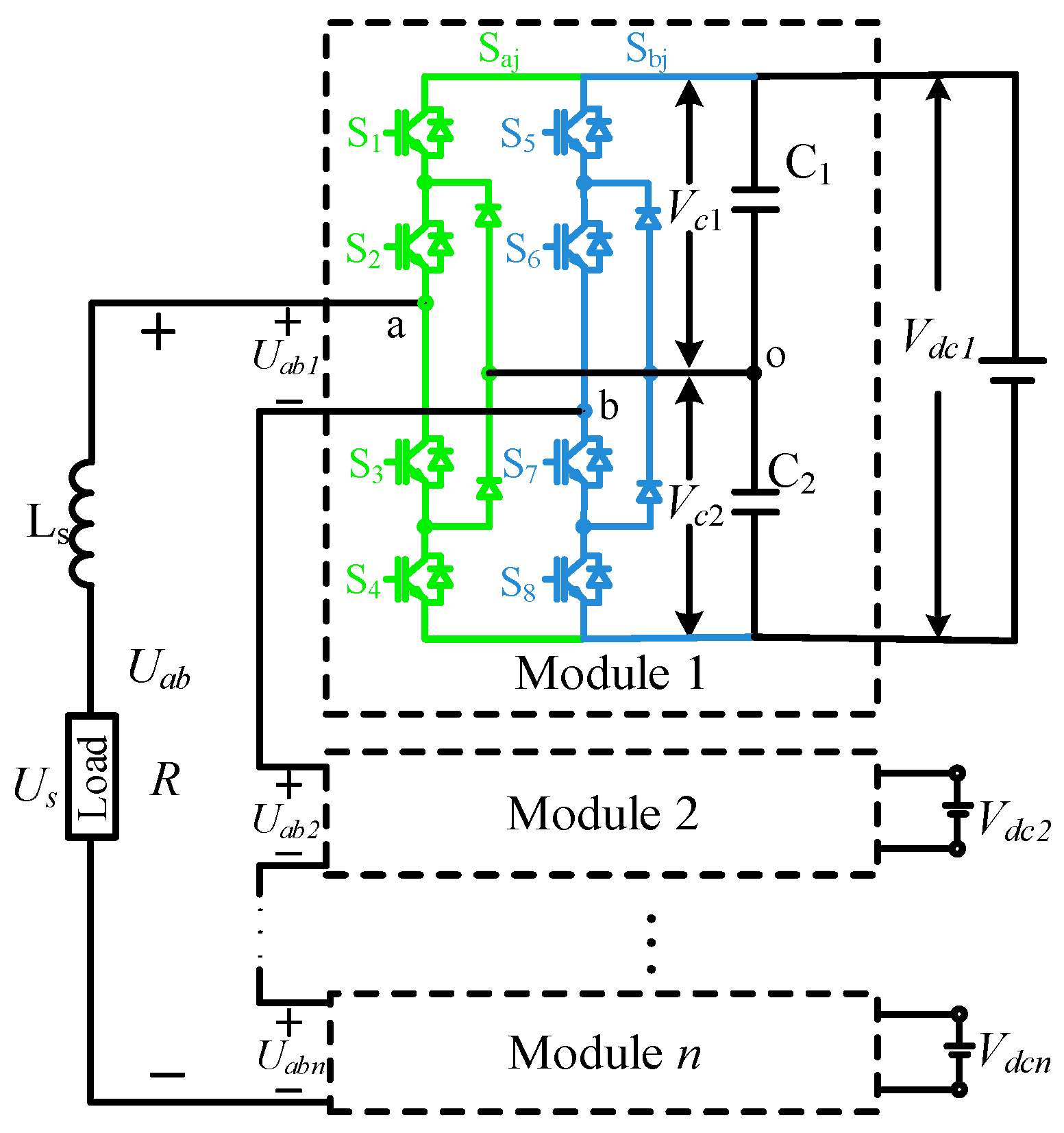
As is illustrated in Figure 1, multi-module 3LNPC-CC is composed of DC input, cascaded modules, and AC output. The AC-link current of each module is the same as other modules because all modules are cascaded.
Three important voltages are shown in Figure 1 including AC-link voltage Us, whole port voltage Uab and each DC-port voltage Vdci. Whole port voltage Uab is the sum of each single module voltage Uabi. Ls is the AC-side inductor which has the function of filter and power transmission. C1 and C2 are two series supporting capacitors in one module. Therefore, the mathematical model of 3LNPC-CC is built on Equations (1)–(3), based on the relationship between each port voltage and switch states of arm bridge.
In Equation (2), Sai and Sbi are bridge arm level and the bridge arm b is the same with bridge arm a. The module-level PWMi is defined by Equation (3), which is a dimensionless variable. It differs from the port voltage Uab by only one amplification factor 2μ while μ is the reciprocal of DC-link voltage Vdci.
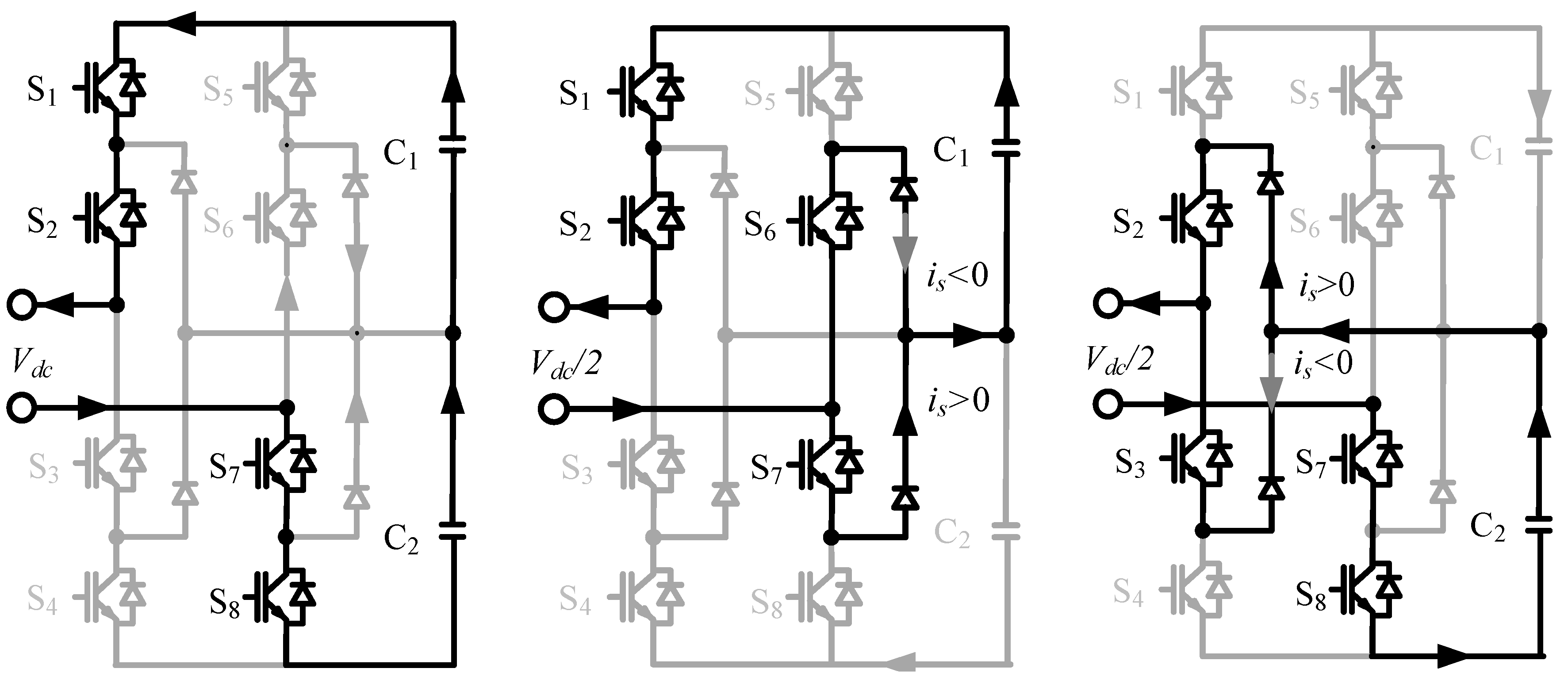
All working modes under single module 3LNPC-CC are illustrated in Figure 2, Figure 3 and Figure 4. According to Equation (2), the bridge arm states determine that 3LNPC-CC has nine working modes. Additionally, each mode can correspond to one module-level PWMi. The operation principles of each mode are as follows when 3LNPC-CC works in inverter mode.
In Mode 1, when Sa = 1 and Sb = −1, the current flow path is built between AC-side load and two capacitors C1 and C2. The result of module-level PWMi is 2 and the port voltage Uabi is Vdc. In this mode, DC-link power is charged to AC-side load while series capacitors C1 and C2 release energy.
In Mode 2, when Sa = 1 and Sb = 0, the current flow path is built between AC-side load and only one capacitor C1. The result of module-level PWMi is 1 and the port voltage Uabi is 0.5Vdc. In this mode, DC-link power continues to be charged to AC-side load. However, capacitor C1 releases energy and capacitor C2 stores energy.
In Mode 3, when Sa = 0 and Sb = 1, the current flow path is built between AC-side load and only one capacitor C2. The result of the module-level is PWMi 1 and the port voltage Uabi is 0.5Vdc, which is similar to Mode 2. In this mode, DC-port power is still charged to AC-side load. However, capacitor C2 releases energy and capacitor C1 stores energy, which has opposite effects compared with Mode 2.
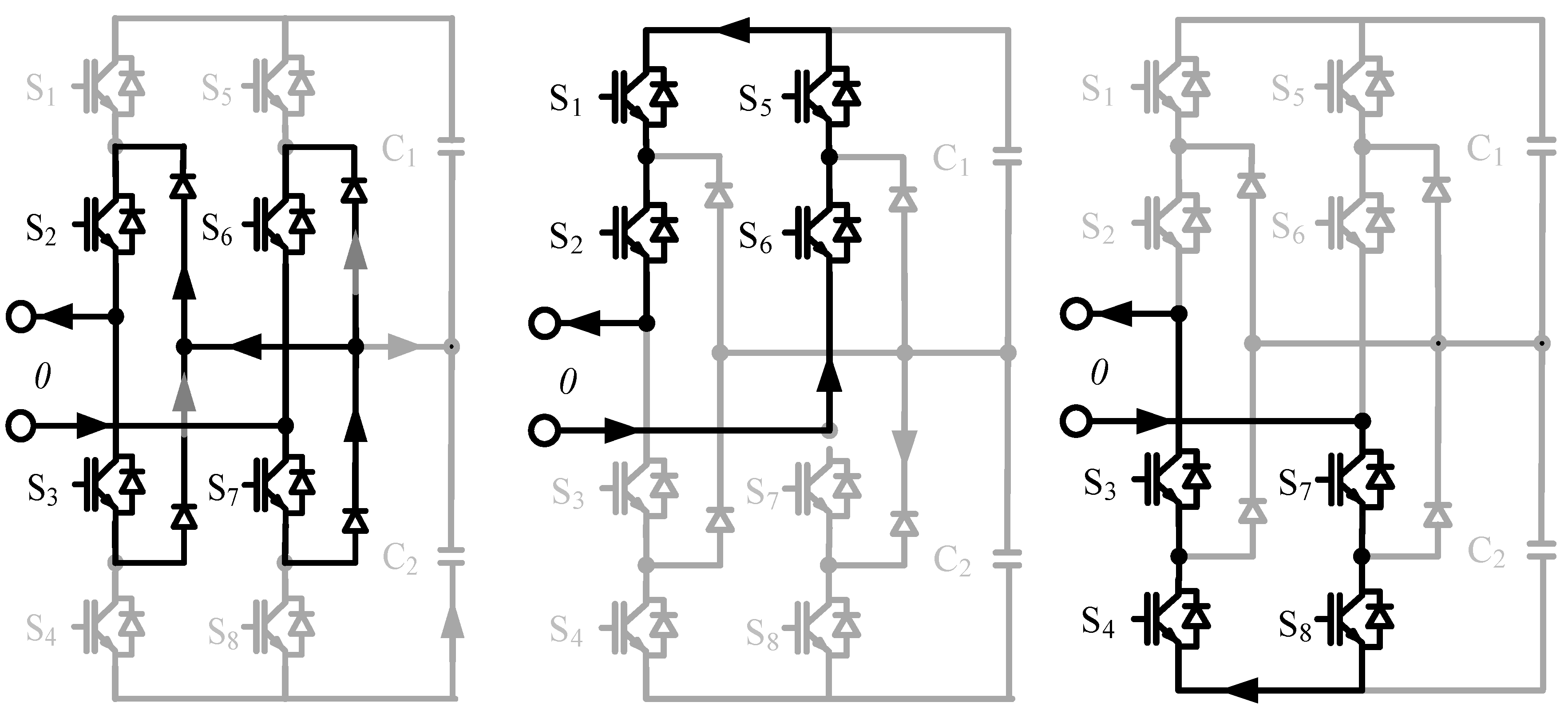
In Mode 4, when Sa = 0 and Sb = 0, the AC-side load is isolated from DC-link voltage. The result of module-level PWMi is 0 and the port voltage Uabi is 0 similarly. In this mode, the AC-side inductor Ls releases energy to the load while the energy of series capacitors keeps constant.
In Mode 5, when Sa = 1 and Sb = 1, the AC-side load is isolated from DC-link voltage. The result of module-level PWMi is 0 and the port voltage Uabi is 0 similarly. In this mode, the AC-side voltage is supported by inductor Ls while the capacitor voltage is determined by DC-link voltage.
In Mode 6, when Sa =−1 and Sb = −1, the AC-side load is also isolated from DC-link voltage. The result of module-level PWMi is 0 and the port voltage Uabi is 0 similarly. In this mode, the AC-side inductor Ls releases energy to the load while the energy of series capacitors keeps constant, which is similar to Mode 4 and Mode 5.
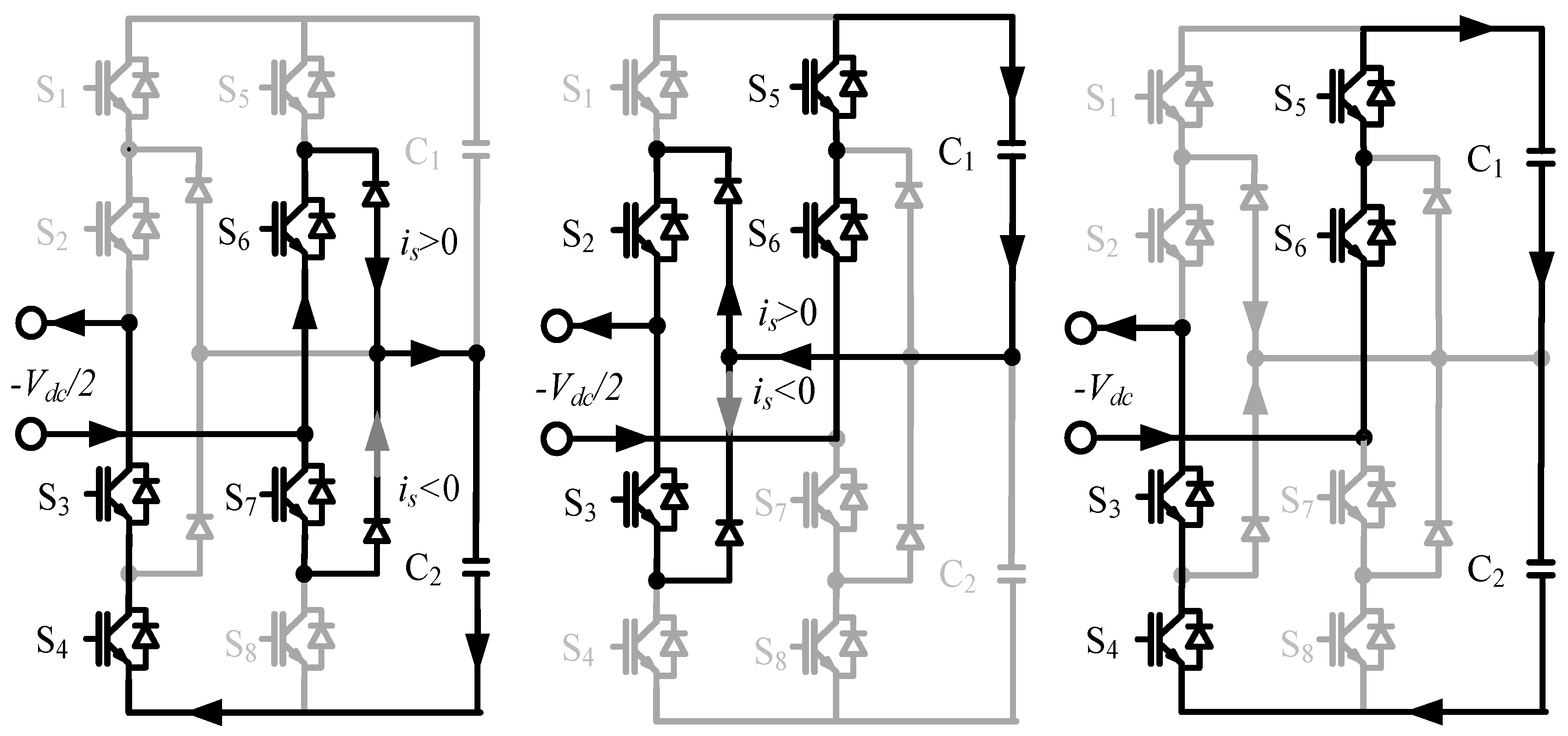
In Mode 7, when Sa = −1 and Sb = 0, the current flow path is built between AC-side load and only one capacitor C2. The result of module-level PWMi is −1 and the port voltage Uabi is −0.5Vdc. In this mode, the energy is transmitted from AC-side load to capacitor C2. Capacitor C1 releases energy while Capacitor C2 stores energy.
In Mode 8, when Sa = 0 and Sb = 1, the current flow path is built between AC-side load and only one capacitor C1. The result of module-level PWMi is −1 and the port voltage Uabi is −0.5Vdc. In this mode, it has similar situations with Mode 7 except for the state of charge or discharge on the capacitor.
In Mode 9, when Sa = −1 and Sb = 1, the current flow path is built between AC-side load and capacitors C1 and C2. The result of module-level is PWMi −2 and the port voltage Uabi is −Vdc, which is the opposite with Mode 1. In this mode, AC-side power is transmitted to DC-link with the charge of both capacitors C1 and C2. Capacitor C1 and C2 store energy at the same time.
2.2. Control Strategy of 3LNPC-CC
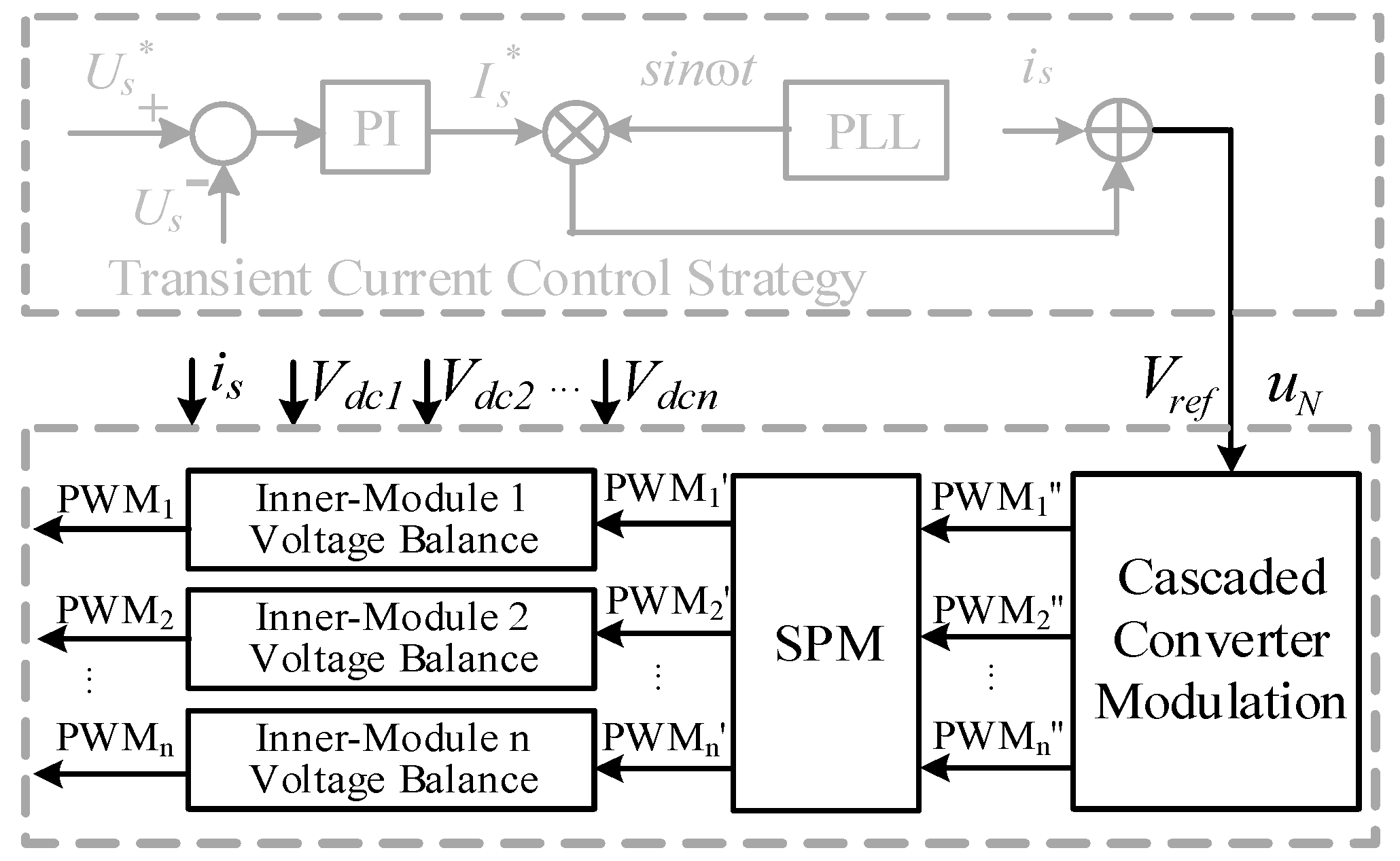
The control strategy and modulation strategy in this paper are illustrated in Figure 5, respectively. To control the output voltage and the output current of the 3LNPC-CC, double closed-loop control is designed. The controller uses the voltage loop and current loop. In the voltage loop, the PI controller is used. The input of PI controller is the error between the given value and real value of the AC-side voltage Us. To decrease the total harmonic distortion (THD) of the Us, the current loop is added as a proportion feedback loop. The phase locked loop (PLL) is used in the current loop to realize phase tracking. The output of the controller, UN, is also the input of the modulation strategy to produce pulse width modulation (PWM) signals. In terms of modulation, firstly, the traditional modulation of 3LNPC-CC is designed. In this paper, the phase shift carrier–space vector pulse width modulation (PSC-SVPWM) is applied to arrange the switch state and power equally for each module when the converter is in normal operation, which is PWM’’ in Figure 5. Then, when the DC-port of one module is a fault, the Sequence Pulse Modulation strategy for 3LNPC-CC which is proposed in this paper has been added, to keep the DC-link voltage-balancing in this situation. The SPM will rearrange the switch state of each module as PWM’. When the module receives the PWM’, it will be revised again to keep capacitors voltage-balancing in one module as PWM. Lastly, the switch state PWM will be sent to the Insulated Gate Bipolar Transistor (IGBT) of each module the synthesize the proper switch state.
2.3. Module-Level Analyses of 3LNPC-CC
Looking to solve the problem of unbalanced DC-link voltage, firstly, the characteristics of various module levels are exhibited in Table 1. According to Formula (3), nine working modes can correspond to five module levels ranging from −2 to 2. When module-level PWMi = ±2, it has strong influence on DC-link voltage; however, it has no influence on unbalanced capacitor voltage. When module-level PWMi = ±1, the influence on DC-link voltage is less than ±2, but the effects on capacitor voltages are obviously stronger than ±2. Besides, module-level PWMi =0 contributes no effects on the converter due to the isolated characteristics of these states.
Based on the analyses of module level, a workable solution to unbalanced voltage within the module and between modules is established by using the lowest level −2 to compensate for the lowest DC-link voltage and using the highest level 2 to adjust the highest DC-link voltage. Besides, switching two different states under module level 1 or −1, the capacitor energy can be exchanged which is the direct solution to capacitor voltage-balancing.
3. Sequence Pulse Modulation Strategy
Due to the structure of the NPC cascaded converter, once the input power of each module is unbalanced, there will inevitably be unbalanced DC voltages among the modules. Such problems can be roughly divided into two categories:
- (1)
- The unbalanced capacitor voltage of inner-module;
- (2)
- The unbalanced capacitor voltage among sub-modules.
Problem (1) has been discussed in detail in Section 2. This problem has been solved by the mutual conversion of four redundant small vectors. The reason for Problem (2) is that in practical application, the input voltage of each module of 3LNPC-CC may be different, resulting in different output power of each module, which leads to unbalanced DC voltage of each capacitor of sub-modules.
The Sequence Pulse Modulation (SPM) studied in this paper makes each sub-module of 3LNPC-CC achieve the DC-link voltage balanced. There are three steps: carrier cascade calculation, sequence pulse generator and rank function. In this paper, for the sake of discussion, a three-module 3LNPC-CC topology is taken as an example to illustrate the working principle of SPM.
3.1. Carrier Cascaded Calculation
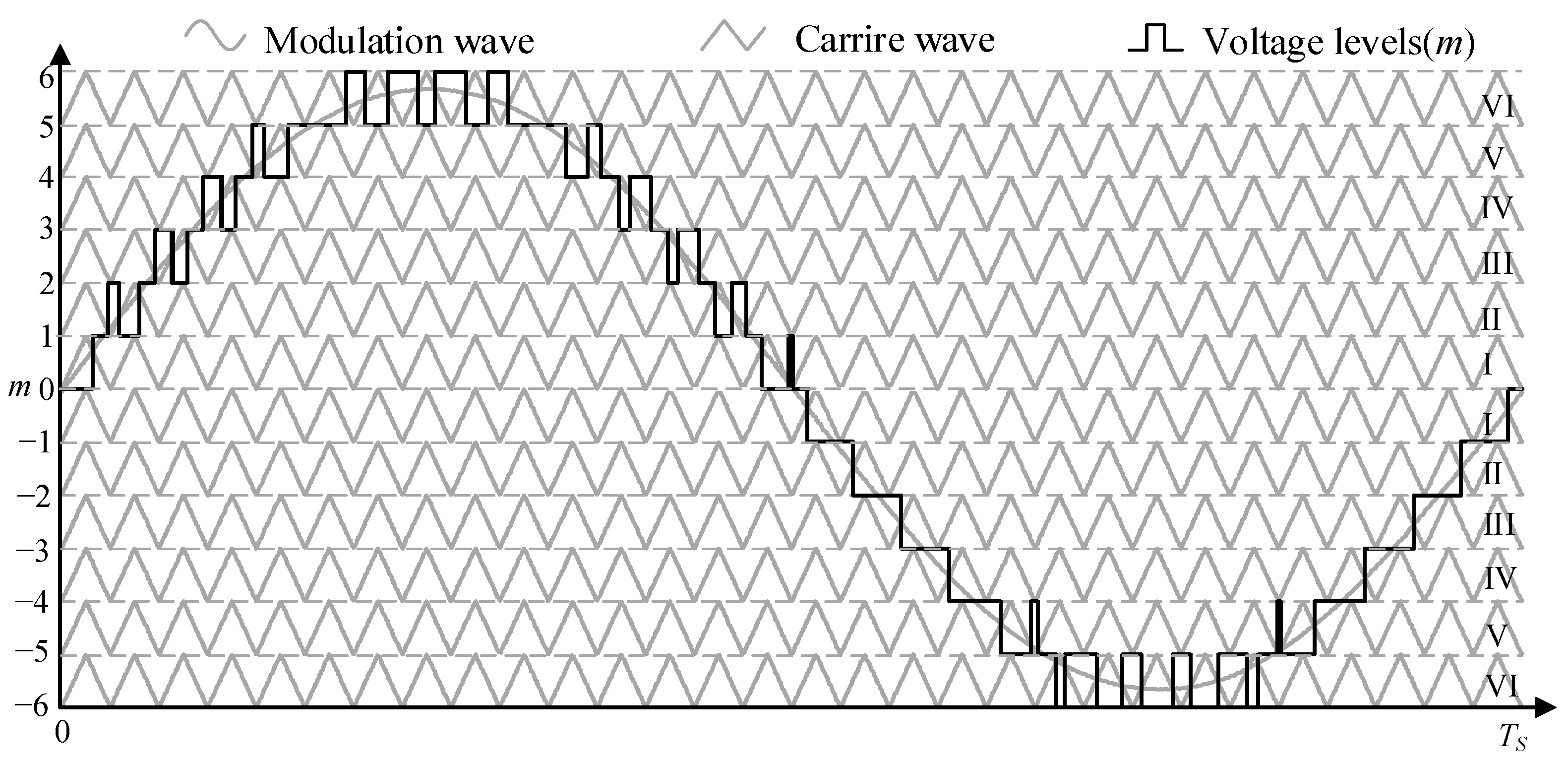
The function of carrier cascaded calculation is to generate modulation wave, and compare the modulation wave with the carrier wave in order to get the voltage level m. The number of the voltage level is determined by the number of cascaded modules of 3LNPC-CC. A three-module 3LNPC-CC studied in this paper will generate 4 × 3 + 1 = 13 levels, which are labeled as I~VI regions as shown in Figure 6.
3.2. Sequence Pulse Generator
The sequence pulse generator is developed to distribute switch state Si. According to the analysis above, switch states ±2 have the strongest voltage-balancing capability. Therefore, a limit condition is considered in which, if all the modules are under the condition that their switch states are 2 or −2, it could achieve the best effect on voltage-balancing among modules. The mathematical model of the sequence pulse generator of n- module 3LNPC-CC is expressed as:
Among these parameters, SSi represents the switching states i (i ∈ [−2, 2]), modulep is the number of modules with Si = p (p ∈ [−2, 2]), n is the cascaded number of 3LNPC-CC, and m is the voltage level produced by carrier cascaded calculation. These parameters follow the restrictions that SSi, modulep, m and n are all natural numbers.
However, if switch states of all modules are supposed to be 2 or −2, Uab can only work with the voltage level of even numbers. Therefore, it is assumed that there is one and the only module in 3LNPC-CC could generate any switch states in ±2, ±1, 0 to make sure that Uab generates the voltage level normally. This module is defined as modulex (x= ±2, ±1, 0), then the Formula (4) can be modified to:
In a three-module 3LNPC-CC system, SS2 = 2, SS-2 = −2. Therefore, Formula (5) can be applied so that:
The DC voltage rank of the module is SS1st < SS2nd < SS3th and the results are shown in Table 2. However, for example, when m changes between 5 and 4, Si may have a sudden change between 2 and 0 while the voltage rank is changed. That is to say, the voltage level jumping phenomenon still exists. Therefore, the rank function of the NPC cascade converter module is needed.
The switch states of the three-module 3LNPC-CC generated by the rank function are illustrated in Table 3. In the above switch states, no matter how the rank of DC voltage changes, when m equals to +6 and 0, there will not be voltage jumping. Therefore, as long as the voltage rank is only allowed to change when m is 0 or ±6, Uab will not change abruptly. Under such circumstances, voltage jumping phenomena are eliminated.
4. Limitation
To explore the limitation of the voltage-balancing, the voltage-balancing ability of SPM is calculated. According to the switching state of sequence pulse modulation strategy based on 3LNPC-CC, the switch working time is calculated according to volt-second balance law, as shown in Table 4. To verify it by simulation and experiment, the calculation result is based on a 3LNPC-CC of three modules.
Based on the fact that a three-module single-phase 3LNPC-CC has six voltage levels in the positive and negative during each half-cycle (excluding zero level), the levels can be divided into six sections. Similarly, according to the switching state selection and switch working time of the six sections, the input power of each module gained in one cycle can be calculated, and the calculation results are as follows (8).
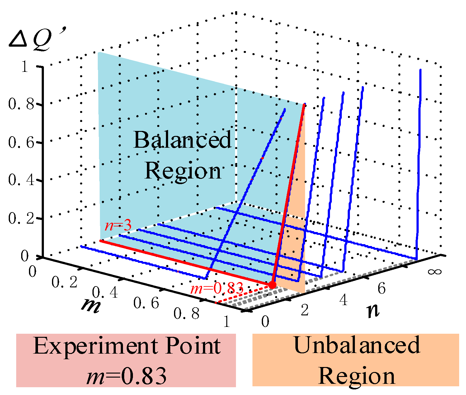
Adding all the power in Formula (8) together, the power of the fault module is calculated. If the result is negative or zero, the capacitor could work normally without power input in this working state, which means the DC-link voltage of the modules could be equal even one of the modules failed. To unify the result under different power levels, the unbalance degree is defined as follows.
where ƊQ′ is the unbalance degree, from 0 to 1. Qi is the energy of the fault module in one period, Qj is the energy of one module in one period when 3LNPC-CC is working normally. Then the result of the calculation is presented in Figure 7. The result shows that in a three-module 3LNPC-CC, it could work normally even if a module suffers from DC-port fault by using SPM, once the modulation is under around 0.83.
5. Simulation
A simulation model was set up by using Matlab/Simulink simulation system. The simulation parameters are covered in Table 5.
In order to validate the correctness of the voltage-balancing strategy for inner-module, 50 Ω and 20 Ω resistors were respectively connected in parallel on the two capacitors C1 and C2 to increase the voltage unbalance of the two capacitors.
As shown in Figure 8, before 0.35 s, the voltage-balancing strategy for the inner-module was not added in the simulation. During this period, the capacitor voltage on the DC side presents a divergent state. After adding the voltage-balancing strategy for inner-module at 0.35 s, the DC side capacitor voltage will converge.
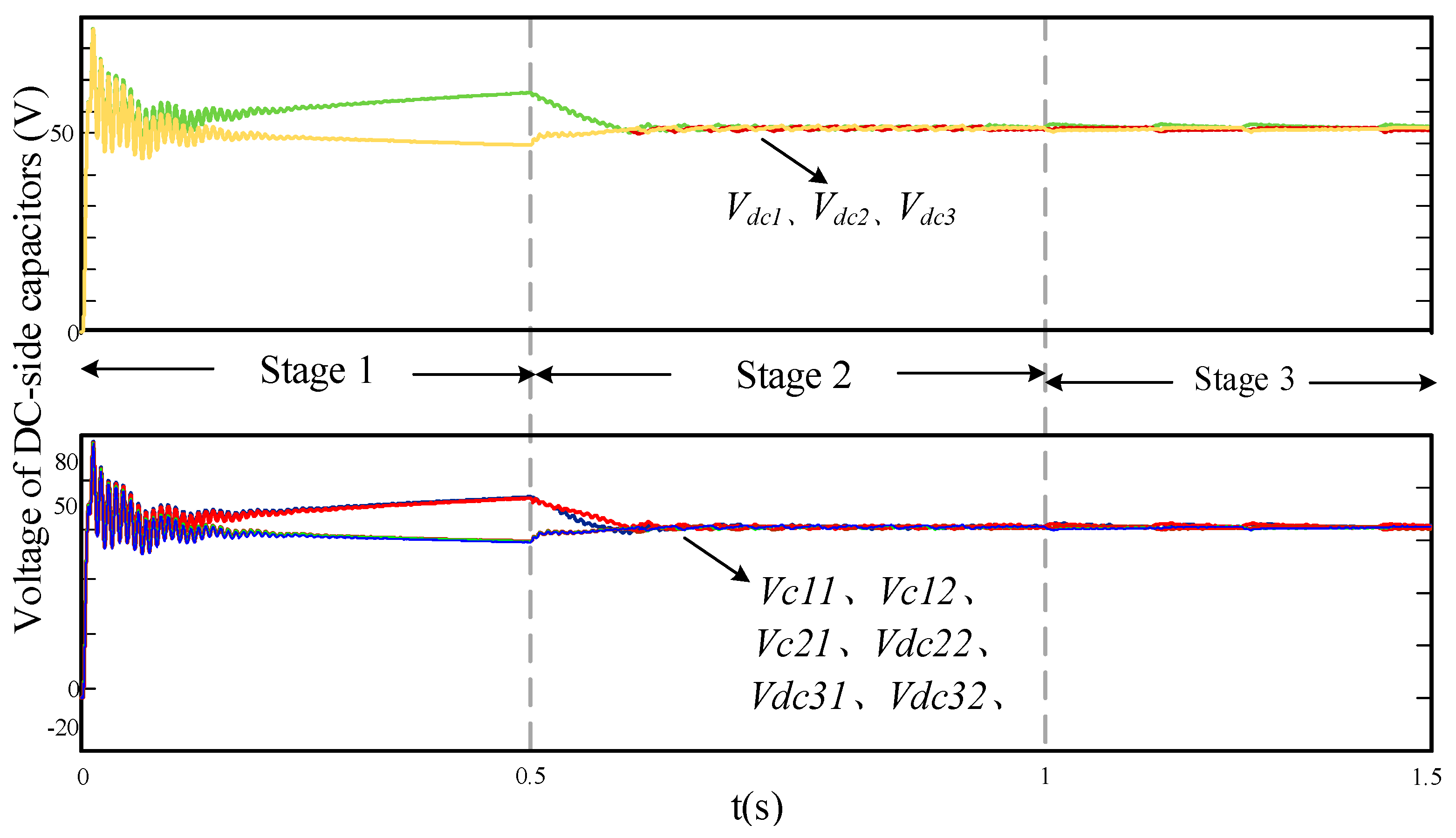
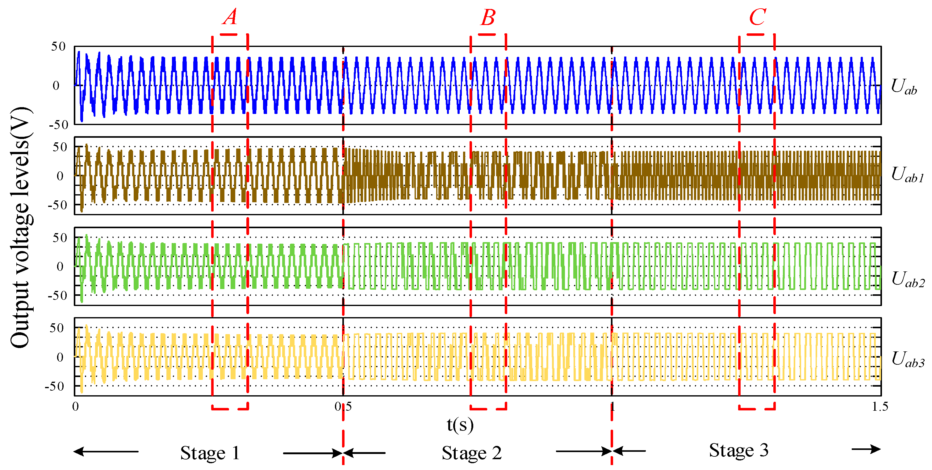
To validate the correctness of voltage-balancing strategy among the sub-modules while the DC-port of one module is a fault, a simulation of three-module 3LNPC-CC was set up. Figure 9 shows DC voltages of the capacitors.
The simulation time is divided into three parts:
Stage 1: during the period of 0 s~0.5 s, Module 1 is the unbalanced module the input voltage of which is set to 50 V. At this time, the SPM modulation strategy is not added in the system, and the DC-link voltage will diverge.
Stage 2: during the period of 0.5 s~1 s, the SPM strategy is added. The DC-link voltages among each module start to converge from the original divergent state.
Stage 3: during the period of 1 s~1.5 s, input voltage mutation is set. At 1 s, Module 1 is set to the module without input voltage. Under the influence of the SPM strategy, the DC-link voltages among each module remain balanced.
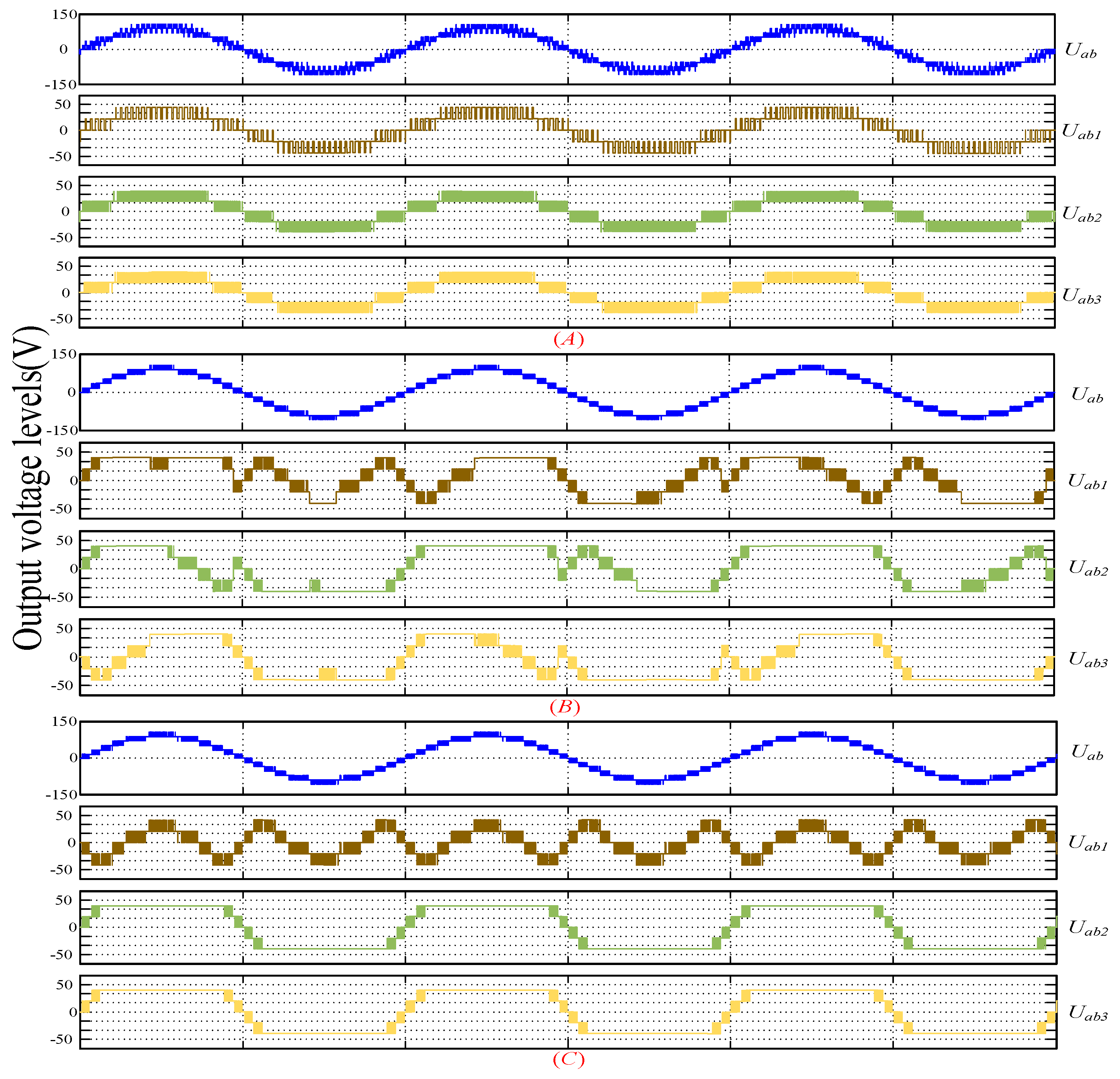
The detailed waveforms of three regions in Figure 10 are shown in Figure 11. The output voltage Uab and each modules’ output voltage Uab1, Uab2 and Uab3 are illustrated. In the figure, (A) shows that before adding the SPM strategy, Uab exhibits a large number of switch state jump problems, which greatly increases the switching frequency. In the figure, (B), Uab does not exhibit the switch state jump problems after adding SPM strategy. In Figure (C), Module 1 is the module without input voltage, and the output voltage of 3LNPC-CC remains unchanged. Figure 10 and Figure 11 show that 3LNPC-CC works normally when the sudden change of input voltage occurs on the basis of SPM strategy.
6. Experimental Section
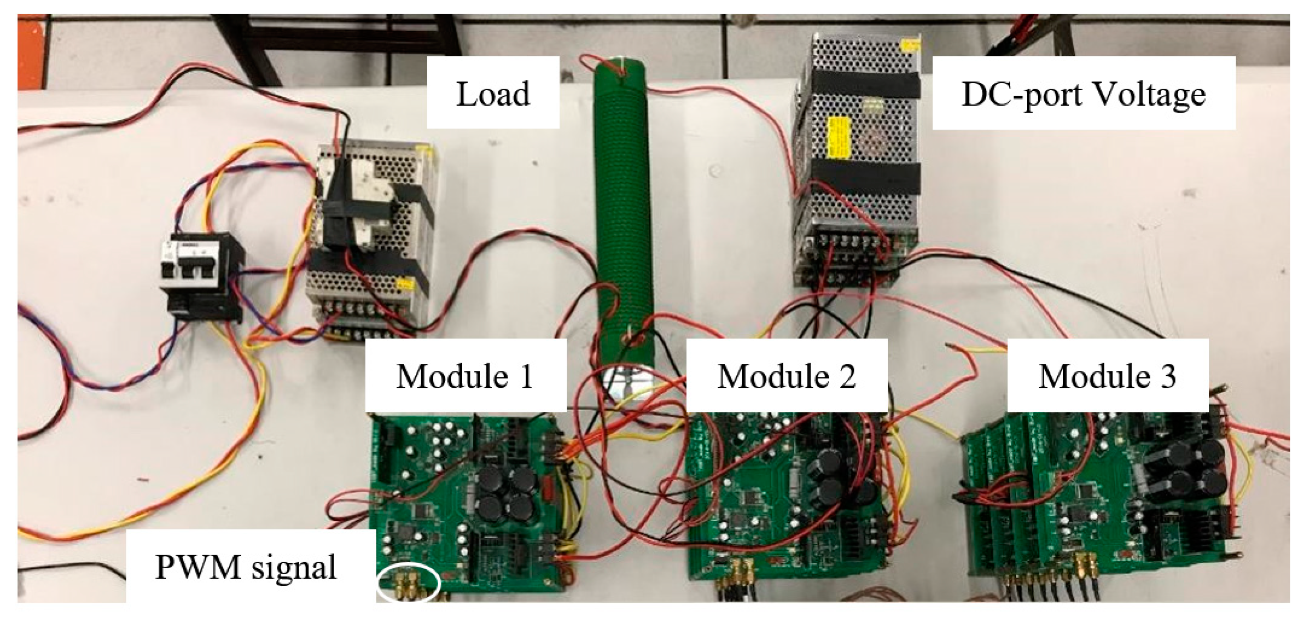
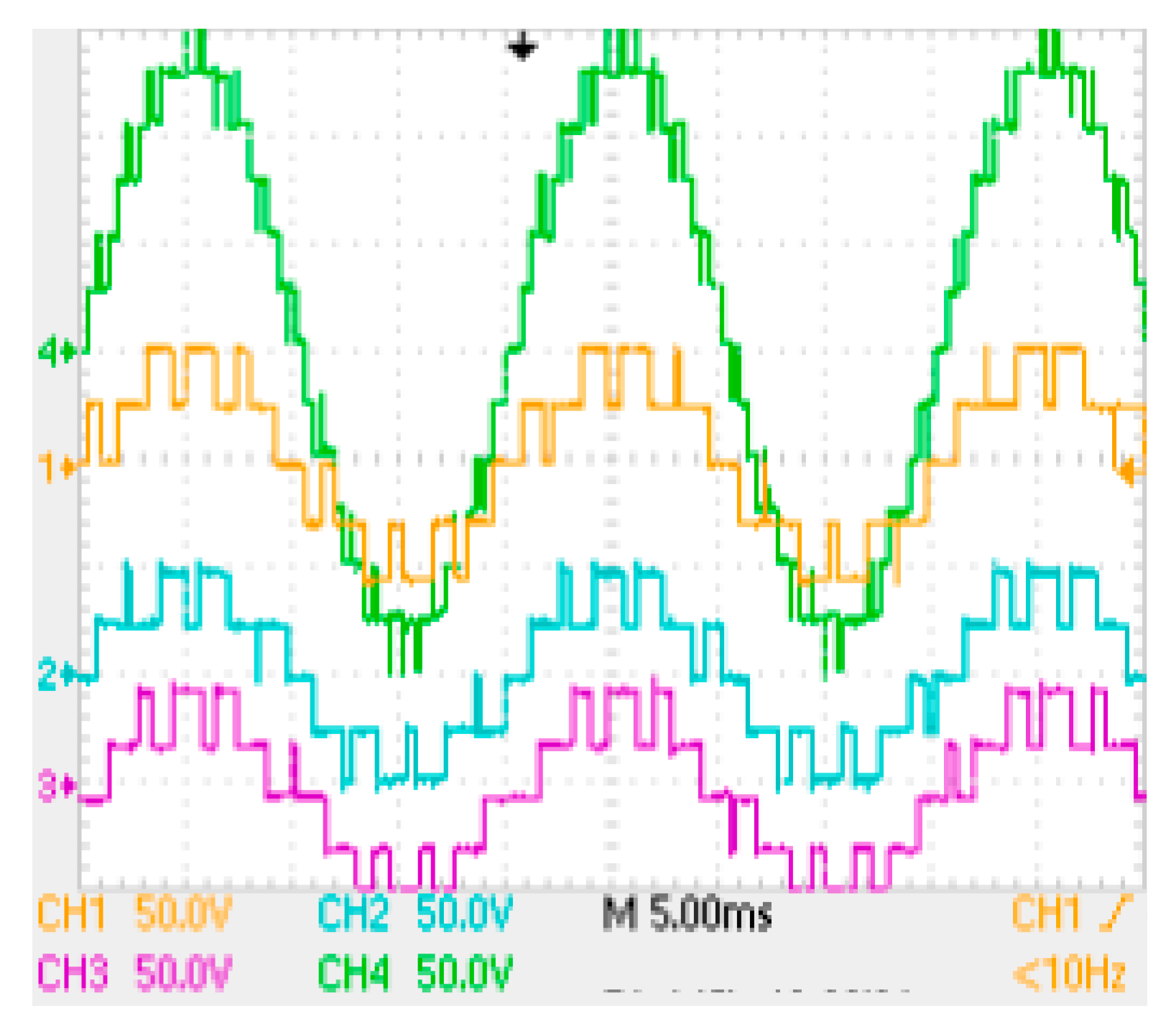
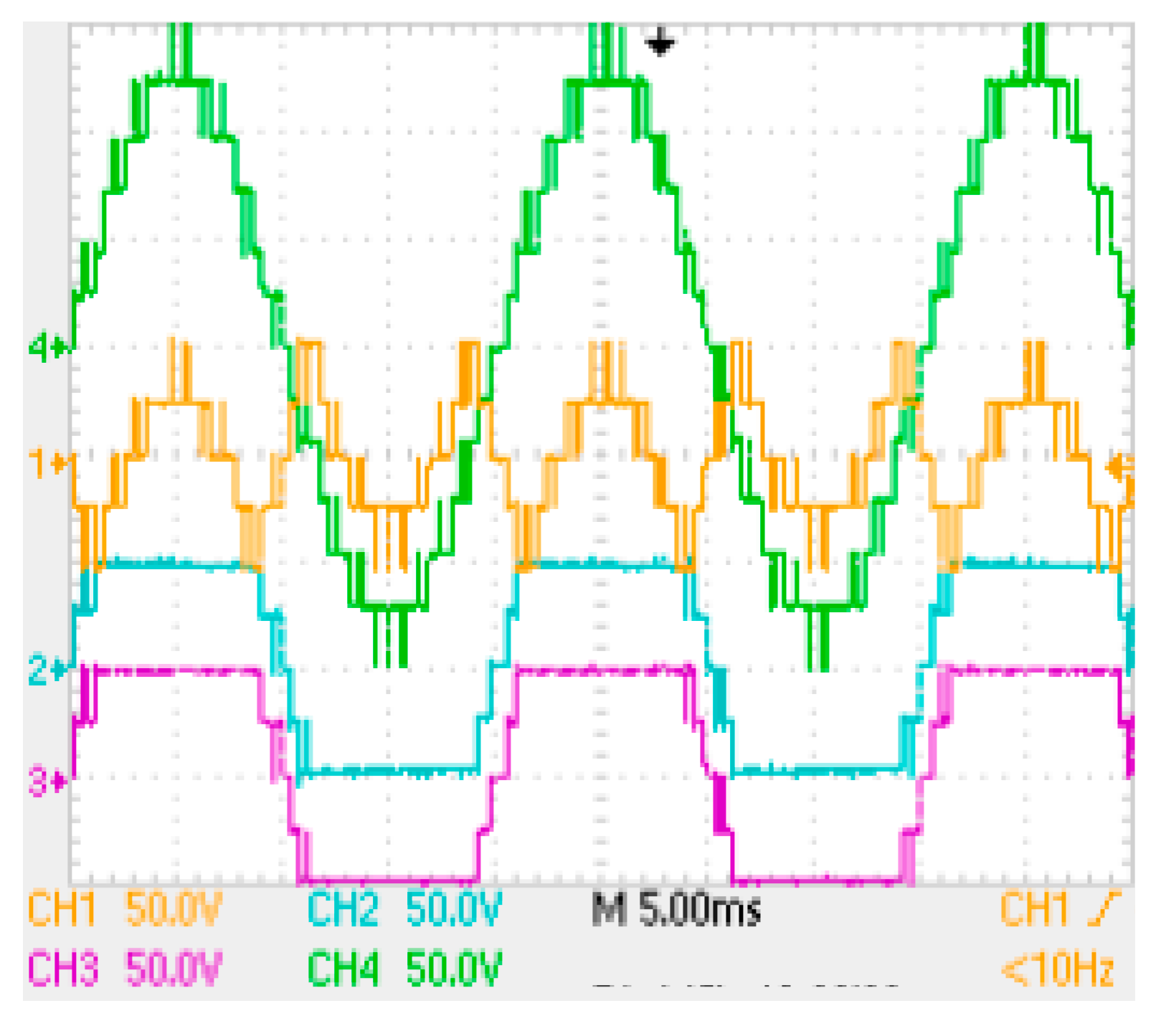
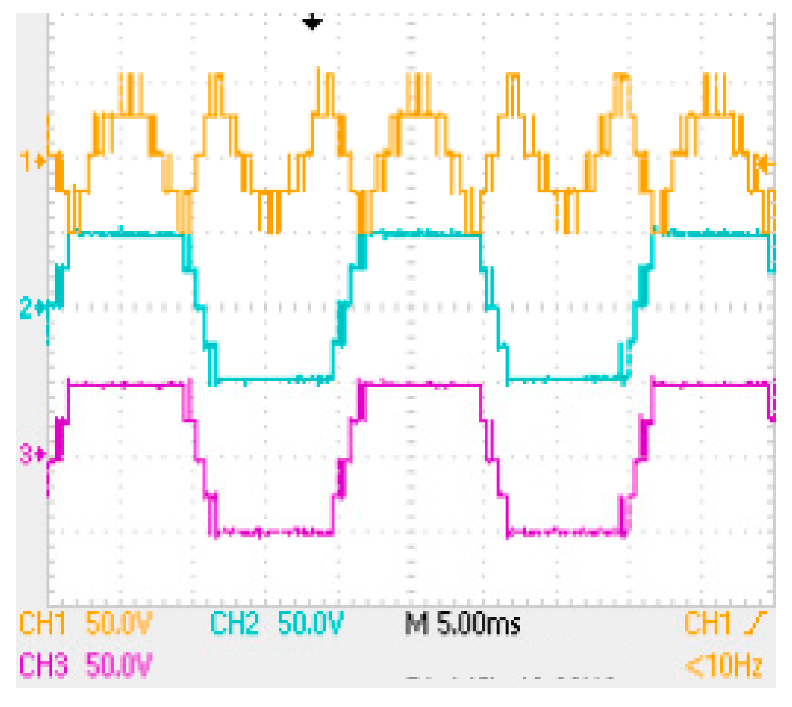
To test the relevant characteristics of the SPM modulation, a three-module prototype was made, as shown in Figure 12. The detailed parameters of the prototype are shown in Table 5. The experiment has been accomplished to verify the strategy. Figure 13 and Figure 14 are the PSC-SVPWM modulation when the 3LNPC-CC works normally; both the switch state and the power are sent equally to the module. Figure 13 and Figure 14 show the proposed SPM modulation; once one module suffers from a DC-port fault, the switch state of fault module changes frequently, in order to charge the capacitor as much as possible. Therefore, the fault module could keep the voltage-balancing, as the energy of the capacitor remains unchanged.
When one module suffers from the DC-port fault, the proposed strategy works to ensure the voltage-balancing on DC-link, as Figure 15 and Figure 16 show. Even with fluctuation appearing, the DC-link voltage recovers to the normal level, and the output voltage works the same as the normal state. Additionally, the fluctuation proved the effect of the SPM, as the DC-link voltage of the fault module keeps equal dynamically.
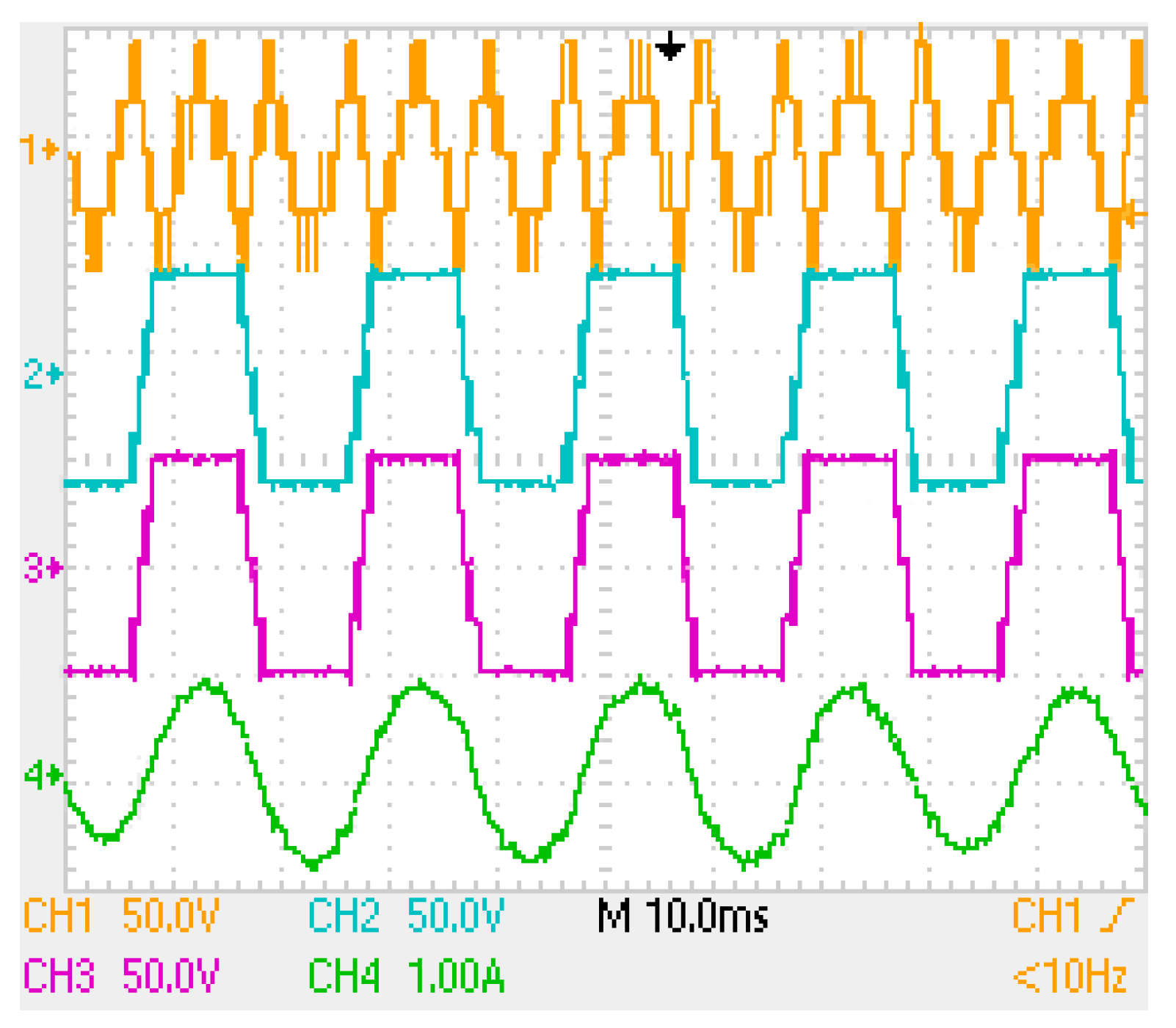
To test the voltage-balancing ability of the SPM, the 3LNPC-CC experiment starts when one module has no DC input, as Figure 17 and Figure 18 show. Figure 17 shows the port voltage of each module and the grid current of the converter, which work normally. Figure 18 is a dynaimic experiment, which shows that the SPM works when the DC-port of one module suffers from fault. However, owing to the SPM, the DC-link voltage of all modules keeps dynamic balance.
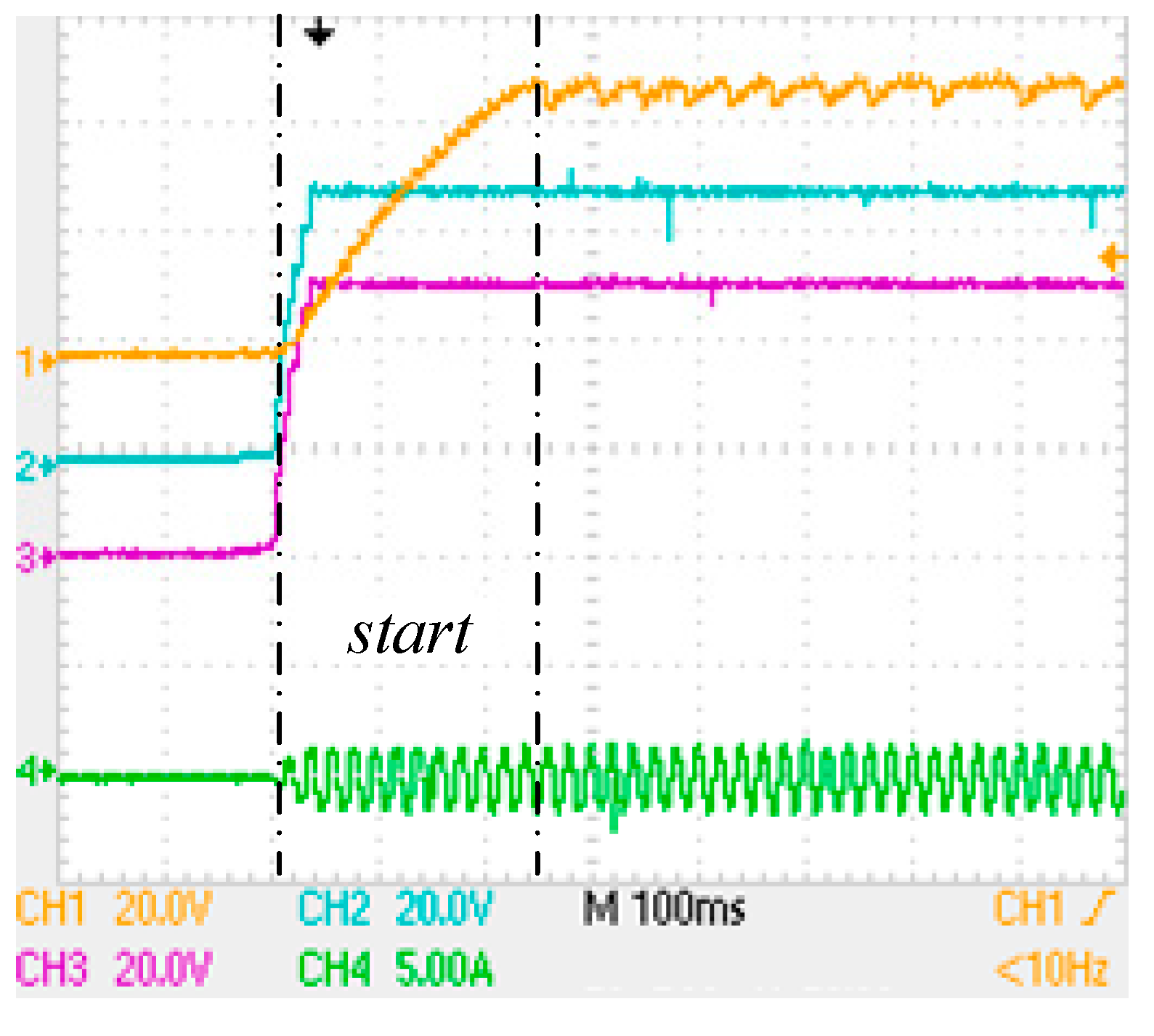
Two other dynamic experiments have been done, as shown in Figure 19 and Figure 20. Figure 19 is the start process when the DC-port fault occurs. Because of the DC-port fault, the start process becomes slow as the fault module needs time to recover. The start process ends with the recovery of the DC-link voltage of the fault module. The experiment shows that the 3LNPC-CC could start after 0.25 s under SPM, which means the SPM has strong voltage-balancing ability. The experiment of Figure 20 is designed as follows: before t1, the 3LNPC-CC works normally by using the PSC modulation. After t1, one module of the converter suffers from a DC-port fault without SPM; therefore, the DC-link voltage of the fault module fails down. At the time of t2, that is, when the fault module reduced the DC-link voltage to half of its previous level, then the SPM was applied. Using SPM, the DC-link voltage rises up to the normal level at t3. The experiment illustrates nice dynamic characteristics of the SPM, as the DC-link voltage recovers to normal in about 75 ms after t2.
7. Conclusions
This paper proposed a voltage-balancing strategy named sequence pulse modulation (SPM) for within a module and among the modules. The structure and mathematic model are discussed, then the SPM strategy and its limitations are elaborated in detail. The simulation and experimental results verify the validity of the theoretical research. The limitation of voltage-balancing ability based on 3LNPC-CC is calculated and the correctness of the strategy is verified by simulation and experiment results. The experiment verified that, under modulation depth of 0.83, a three-module 3LNPC-CC could work normally once one module has no DC power supply. By carrier cascaded calculation, sequence pulse generator and rank function, the SPM could achieve the following goals: 1. to keep the DC-link voltage steady while one DC-port module of the 3LNPC-CC failed; 2. to ensure a smooth change of voltage level while keeping the output voltage balanced; 3. to feature a strong voltage-balancing capability; 4. to be easy to employ in the n-module system.
Author Contributions
All the authors contributed to this work. L.Y. and X.P. analyzed the strategy and conceived the experiment; X.P. performed the experiment; L.Y. wrote the paper; S.G. analyzed the data; X.P. and L.Y. contributed the experimental prototype.
Funding
This work was supported by the National Natural Science Foundations of China (Grant No.U1734202) and National Key R&D Program of China (No. 2018YFC0809500).
Conflicts of Interest
The authors declare no conflict of interest.
References
- Yang, S.Y.; Bryant, A.; Mawby, P.; Xiang, D.W.; Ran, L.; Tavner, P. An industry-based survey of reliability in power electronic converters. In Proceedings of the IEEE Energy Conversion Congress and Exposition, San Jose, CA, USA, 20–24 September 2009. [Google Scholar]
- Peng, T.; Dan, H.B.; Yang, J.; Deng, H.; Zhu, Q.; Wang, C.S.; Gui, W.H.; Guerrero, J.M. Open-Switch Fault Diagnosis and Fault Tolerant for Matrix Converter with Finite Control Set-Model Predictive Control. IEEE Trans. Ind. Electron. 2016, 63, 5953–5963. [Google Scholar] [CrossRef]
- Choi, J.H.; Kim, S.; Yoo, D.S.; Kim, K.H. A Diagnostic Method of Simultaneous Open-Switch Faults in Inverter-Fed Linear Induction Motor Drive for Reliability Enhancement. IEEE Trans. Ind. Electron. 2014, 62, 4065–4077. [Google Scholar] [CrossRef]
- Ge, X.L.; Pu, J.K.; Gou, B.; Liu, Y.C. An Open-Circuit Fault Diagnosis Approach for Single-Phase Three-Level Neutral-Point-Clamped Converters. IEEE Trans. Power Electron. 2017, 33, 2559–2570. [Google Scholar] [CrossRef]
- Lamb, J.; Mirafzal, B. Open-Circuit IGBT Fault Detection and Location Isolation for Cascaded Multilevel Converters. IEEE Trans. Ind. Electron. 2017, 64, 4846–4856. [Google Scholar] [CrossRef]
- Gautam, S.P.; Kumar, L.; Gupta, S.; Agrawal, N. A Single-Phase Five-Level Inverter Topology with Switch Fault-Tolerance Capabilities. IEEE Trans. Ind. Electron. 2016, 64, 2004–2014. [Google Scholar] [CrossRef]
- Choi, U.M.; Lee, K.B.; Blaabjerg, F. Diagnosis and Tolerant Strategy of an Open-Switch Fault for T-Type Three-Level Inverter Systems. IEEE Trans. Ind. Appl. 2013, 50, 495–508. [Google Scholar] [CrossRef]
- Gou, B.; Ge, X.; Wang, S.; Feng, X.; Kuo, J.B.; Habetler, T.G. An open-switch fault diagnosis method for single-phase PWM rectifier using a model-based approach in high-speed railway electrical traction drive system. IEEE Trans. Power Electron. 2016, 31, 3816–3826. [Google Scholar] [CrossRef]
- Dujic, D.; Zhao, C.H.; Mester, A.; Steinke, J.K.; Weiss, M.; Lewdeni-Schmid, S.; Chaudhuri, T.; Stefanutti, P. Power Electronic Traction Transformer-Low Voltage Prototype. IEEE Trans. Power Electron. 2013, 28, 5522–5534. [Google Scholar] [CrossRef]
- Peng, X.; He, X.; Han, P.; Lin, H.; Gao, S.; Shu, Z. Opposite Vector Based Phase Shift Carrier Space Vector Pulse Width Modulation for Extending the Voltage Balance Region in Single-Phase 3LNPC Cascaded Rectifier. IEEE Trans. Power Electron. 2017, 32, 7381–7393. [Google Scholar] [CrossRef]
- She, X.; Huang, A.Q. Current Sensorless Power Balance Strategy for DC/DC Converters in a Cascaded Multilevel Converter Based Solid State Transformer. IEEE Trans. Power Electron. 2013, 29, 17–22. [Google Scholar] [CrossRef]
- Sim, H.W.; Lee, J.S.; Lee, K.B. Detecting open-switch faults: Using asymmetric zero-voltage switching states. IEEE Ind. Appl. Mag. 2016, 22, 27–37. [Google Scholar] [CrossRef]
- Peng, X.; He, X.; Han, P.; Guo, A.; Shu, Z.; Gao, S. Smooth Switching Technique for Voltage Balance Management Based on Three-Level Neutral Point Clamped Cascaded Rectifier. Energies 2016, 9, 803. [Google Scholar] [CrossRef]
- Yang, S.Y.; Xiang, D.W.; Bryant, A.; Mawby, P.; Ran, L.; Tavner, P. Condition monitoring for device reliability in power electronic converters: A review. IEEE Trans. Power Electron. 2010, 25, 2734–2752. [Google Scholar] [CrossRef]
- Nicolas-Apruzzese, J.; Busquets-Monge, S.; Bordonau, J.; Alepuz, S.; Calle-Prado, A. Analysis of the Fault-Tolerance Capacity of the Multilevel Active-Clamped Converter. IEEE Trans. Ind. Electron. 2012, 60, 4773–4783. [Google Scholar] [CrossRef]
- Chen, A.; Hu, L.; Chen, L.; Deng, Y.; Yao, G.; He, X.N. A Multilevel Converter Topology with Fault-Tolerant Ability. In Proceedings of the Nineteenth Annual IEEE Applied Power Electronics Conference and Exposition, Anaheim, CA, USA, 27 September 2004. [Google Scholar]
- Shu, Z.L.; He, X.Q.; Wang, Z.Y.; Qiu, D.Q.; Jing, Y.Z. Voltage Balancing Approaches for Diode-Clamped Multilevel Converters Using Auxiliary Capacitor-Based Circuits. IEEE Trans. Power Electron. 2012, 28, 2111–2124. [Google Scholar] [CrossRef]
- Shu, Z.L.; Zhu, H.F.; He, X.Q.; Ding, N.; Jing, Y.Z. One-inductor-based auxiliary circuit for dc-link capacitor voltage equalisation of diode-clamped multilevel converter. IET Power Electron. 2013, 6, 1339–1349. [Google Scholar] [CrossRef]
- Zhu, H.F.; Shu, Z.L.; Gao, F.H.; Qin, B.; Gao, S.B. Five-level diode-clamped active power filter using voltage space vector-based indirect current and predictive harmonic control. IET Power Electron. 2014, 7, 713–723. [Google Scholar] [CrossRef]
- Antonio, D.; Marco, L.; Vito Giuseppe, M.; Paola, R. Overview of PI-Based Solutions for the Control of DC Buses of a Single-Phase H-Bridge Multilevel Active Rectifier. IEEE Ind. Appl. Mag. 2008, 44, 857–866. [Google Scholar] [CrossRef]
- Morteza, M.; Ghias, F.; Hossein, I.; Seyed Mohammad, S. A Voltage Balancing Strategy with Extended Operating Region for Cascaded H-Bridge Converters. IEEE Trans. Power Electron. 2014, 29, 5044–5053. [Google Scholar] [CrossRef]
- She, X.; Huang, A.Q.; Wang, G. 3-D Space Modulation with Voltage Balancing Capability for a Cascaded Seven-Level Converter in a Solid-State Transformer. IEEE Trans. Power Electron. 2011, 26, 3778–3789. [Google Scholar] [CrossRef]
- Peng, X.; He, X.; Han, P.; Lin, X.; Shu, Z.; Gao, S. Sequence Pulse Modulation for Voltage Balance in a Cascaded H-Bridge Rectifier. J. Power Electron. 2017, 17, 664–673. [Google Scholar] [CrossRef]
- Lin, H.; Shu, Z.; He, X.; Liu, M. N-D SVPWM with DC Voltage Balancing and Vector Smooth transition Algorithm for Cascaded Multilevel Converter. IEEE Trans. Ind. Electron. 2018, 65, 3837–3847. [Google Scholar] [CrossRef]
- Han, P.; He, X.; Zhao, Z.; Yu, H.; Wang, Y.; Peng, X.; Shu, Z. DC-Link Capacitor Voltage Balanced Modulation Strategy Based on Three Level Neutral Point Clamped Cascaded Rectifier. J. Power Electron. 2019, 19, 99–107. [Google Scholar] [CrossRef]
- Yu, Y.; Konstantinou, G.; Hredzak, B.; Agelidis, V.G. Power Balance of Cascaded H-Bridge Multilevel Converters for Large-Scale Photovoltaic Integration. IEEE Trans. Power Electron. 2016, 31, 292–303. [Google Scholar] [CrossRef]
- Li, Y.; Wang, Y.; Li, B.Q. Generalized Theory of Phase-Shifted Carrier PWM for Cascaded H-Bridge Converters and Modular Multilevel Converters. IEEE J. Emerg. Sel. Top. Power Electron. 2016, 4, 589–605. [Google Scholar] [CrossRef]
- Sergio, B.M.; Griñó, R.; Nicolas-Apruzzese, J.; Bordonau, J. Decoupled DC-Link Capacitor Voltage Control of DC–AC Multilevel Multileg Converters. IEEE Trans. Ind Electron. 2016, 63, 1344–1349. [Google Scholar] [CrossRef]
- Li, J.; Georgios, K.; Harith, R.W.; Christopher, D.T.; Josep, P. Capacitor Voltage Reduction in Modular Multilevel Converters under Grid Voltages Unbalances. IEEE Trans. Power Deliv. 2019. [Google Scholar] [CrossRef]
- Jean-Michel, D.P.; Caio, R.D.; Humberto, P.; Fernanda, D.M. Phase Disposition Modulation with Sorting Algorithm for Symmetrical Cascaded Multilevel Converters. IEEE Trans. Ind Appl. 2019. [Google Scholar] [CrossRef]
- Han, P.; He, X.; Ren, H.; Wang, Y.; Peng, X.; Shu, Z.; Gao, S.; Wang, Y.B.; Chen, Z. Fault Diagnosis and System Reconfiguration Strategy of a Single-Phase Three-Level Neutral-Point-Clamped Cascaded Inverter. IEEE Trans. Ind. Appl. 2019, 55, 3863–3876. [Google Scholar] [CrossRef]
Figure 1.
Topology of 3LNPC-CC.

Figure 2.
Mode 1, Mode 2 and Mode 3 of 3LNPC-CC (uab= Vdc, uab= 0.5Vdc).

Figure 3.
Mode 4, Mode 5 and Mode 6 of 3LNPC-CC (uab= 0).

Figure 4.
Work state of 3LNPC-CC (uab = −0.5Vdc, uab = −Vdc).

Figure 5.
The control and modulation strategy of multi-module 3LNPC-CC.

Figure 6.
Carrier Cascaded Calculation for 3LNPC-CC.

Figure 7.
Voltage-balancing ability calculation.

Figure 8.
The waveform of capacitors’ voltage on DC-link.

Figure 9.
The waveform of capacitors’ voltage on DC-link.

Figure 10.
The output voltage levels waveforms of 3LNPC-CC.

Figure 11.
The detailed output voltage levels waveforms of 3LNPC-CC.

Figure 12.
Three-module prototype of 3LNPC-CC.

Figure 13.
Switch states of PSC-SVPWM. (CH1: port voltage of Module 1; CH2: port voltage of Module 2; CH3: port voltage of Module 3; CH4: whole port voltage).
Figure 13.
Switch states of PSC-SVPWM. (CH1: port voltage of Module 1; CH2: port voltage of Module 2; CH3: port voltage of Module 3; CH4: whole port voltage).

Figure 14.
Switch states of PSC-SVPWM. (CH1: port voltage of Module 1; CH2: port voltage of Module 2; CH3: port voltage of Module 3; CH4: whole port voltage ).
Figure 14.
Switch states of PSC-SVPWM. (CH1: port voltage of Module 1; CH2: port voltage of Module 2; CH3: port voltage of Module 3; CH4: whole port voltage ).

Figure 15.
Switch states of Proposed strategy. (CH1: port voltage of Module 1; CH2: port voltage of Module 2; CH3: port voltage of Module 3; CH4: whole port voltage).
Figure 15.
Switch states of Proposed strategy. (CH1: port voltage of Module 1; CH2: port voltage of Module 2; CH3: port voltage of Module 3; CH4: whole port voltage).

Figure 16.
Switch states of Proposed strategy. (CH1: port voltage of Module 1; CH2: port voltage of Module 2; CH3: port voltage of Module 3; CH4: whole port voltage).
Figure 16.
Switch states of Proposed strategy. (CH1: port voltage of Module 1; CH2: port voltage of Module 2; CH3: port voltage of Module 3; CH4: whole port voltage).

Figure 17.
DC-port fault when SPM applied. (CH1: port voltage of Module 1; CH2: port voltage of Module 2; CH3: port voltage of Module 3; CH4: AC-link current of cascaded modules.).
Figure 17.
DC-port fault when SPM applied. (CH1: port voltage of Module 1; CH2: port voltage of Module 2; CH3: port voltage of Module 3; CH4: AC-link current of cascaded modules.).

Figure 18.
Dynamic performance when SPM applied. (CH1: DC-link voltage of Module 1; CH2: DC-link voltage of Module 2; CH3: DC-link voltage of Module 3; CH4: AC-link current of cascaded modules).
Figure 18.
Dynamic performance when SPM applied. (CH1: DC-link voltage of Module 1; CH2: DC-link voltage of Module 2; CH3: DC-link voltage of Module 3; CH4: AC-link current of cascaded modules).

Figure 19.
Start the experiment when SPM applied. (CH1: DC-link voltage of Module 1; CH2: DC-link voltage of Module 2; CH3: DC-link voltage of Module 3; CH4: AC-link current of cascaded modules).
Figure 19.
Start the experiment when SPM applied. (CH1: DC-link voltage of Module 1; CH2: DC-link voltage of Module 2; CH3: DC-link voltage of Module 3; CH4: AC-link current of cascaded modules).

Figure 20.
Dynamic experiment. (CH1: DC-link voltage of Module 1; CH2: DC-link voltage of Module 2; CH3: DC-link voltage of Module 3; CH4: AC-link current of cascaded modules).
Figure 20.
Dynamic experiment. (CH1: DC-link voltage of Module 1; CH2: DC-link voltage of Module 2; CH3: DC-link voltage of Module 3; CH4: AC-link current of cascaded modules).


Table 1.
Characteristics of module levels.
| PWMi | Sai | Sbi | C1i | C2i | DC-link |
|---|---|---|---|---|---|
| 2 | 1 | −1 | discharge | discharge | discharge |
| 1 | 1 | 0 | discharge | ||
| 0 | −1 | discharge | |||
| 0 | 1 | 1 | |||
| 0 | 0 | ||||
| −1 | −1 | ||||
| −1 | −1 | 0 | charge | ||
| 0 | 1 | charge | |||
| −2 | −1 | 0 | charge | charge | charge |
Table 2.
N-Module 3LNPC Converter Switch States.
| m | SS1st | SS2nd | SS3th |
|---|---|---|---|
| 6 | 2 | 2 | 2 |
| 5 | 2 | 2 | 1 |
| 4 | 2 | 2 | 0 |
| 3 | 2 | 2 | −1 |
| 2 | 2 | 2 | −2 |
| 1 | 2 | 1 | −2 |
| 0 | 2 | 0 | −2 |
| −1 | 2 | −1 | −2 |
| −2 | 2 | −2 | −2 |
| −3 | 1 | −2 | −2 |
| −4 | 0 | −2 | −2 |
| −5 | −1 | −2 | −2 |
| −6 | −2 | −2 | −2 |
Table 3.
Module 3LNPC Converter Switch States.
| m | SS1st | SS2nd | SS3th |
|---|---|---|---|
| 6 | 2 | 2 | 2 |
| 5 | 2 | 2 | 1 |
| 4 | 2 | 2 | 0 |
| 3 | 2 | 2 | −1 |
| 2 | 2 | 2 | −2 |
| 1 | 1 | 1 | −1 |
| 0 | 0 | 0 | 0 |
| −1 | −1 | −1 | 1 |
| −2 | −2 | −2 | 2 |
| −3 | −2 | −2 | 1 |
| −4 | −2 | −2 | 0 |
| −5 | −2 | −2 | −1 |
| −6 | −2 | −2 | −2 |
Table 4.
Switch working time of a 3LNPC-CR.
| M | Ta | Tb |
|---|---|---|
| I | (1–6Msin(ωt))Ts | (6Msin(ωt))Ts |
| II | (2–6Msin(ωt)) Ts | (6Msin(ωt)−1)Ts |
| III | (3–6Msin(ωt))Ts | (6Msin(ωt)−2)Ts |
| IV | (4–6Msin(ωt))Ts | (6Msin(ωt)−3)Ts |
| V | (5–6Msin(ωt))Ts | (6Msin(ωt)−4)Ts |
| VI | (6–6Msin(ωt))Ts | (6Msin(ωt)−5)Ts |
Table 5.
Prototype Parameter.
| Parameter Name | Parameter Value | Numbers |
|---|---|---|
| Filter capacitor | 10 μF | 1 |
| Filter inductance | 5 mL | 1 |
| DC-link voltage (Vdc) | 50 V | 3 |
| DC-link capacitor | 470 μF | 3 |
| Carrier wave frequency | 750 Hz | - |
| Modulation depth | 0.83 | - |
| Number of modules | 3 | - |
| Load of 3LNPC-CC | 50 Ω | 1 |
© 2019 by the authors. Licensee MDPI, Basel, Switzerland. This article is an open access article distributed under the terms and conditions of the Creative Commons Attribution (CC BY) license (http://creativecommons.org/licenses/by/4.0/).
Share and Cite
MDPI and ACS Style
Yu, L.; Peng, X.; Gao, S. Voltage-Balancing Strategy for Three-Level Neutral Point Clamped Cascade Converter under Sequence Pulse Modulation. Energies 2019, 12, 3829. https://doi.org/10.3390/en12203829
AMA Style
Yu L, Peng X, Gao S. Voltage-Balancing Strategy for Three-Level Neutral Point Clamped Cascade Converter under Sequence Pulse Modulation. Energies. 2019; 12(20):3829. https://doi.org/10.3390/en12203829
Chicago/Turabian StyleYu, Le, Xu Peng, and Shibin Gao. 2019. "Voltage-Balancing Strategy for Three-Level Neutral Point Clamped Cascade Converter under Sequence Pulse Modulation" Energies 12, no. 20: 3829. https://doi.org/10.3390/en12203829
Note that from the first issue of 2016, this journal uses article numbers instead of page numbers. See further details here.