Building an Organic Solar Cell: Fundamental Procedures for Device Fabrication
by
 ,
,
Katerina Anagnostou
1, 
Minas M. Stylianakis
1,* ,
,
Konstantinos Petridis
1,2,* and
Emmanuel Kymakis
1
1
Center of Materials Technology and Photonics, Department of Electrical and Computer Engineering, Hellenic Mediterranean University (HMU), 71004 Heraklion, Greece
2
Department of Electronic Engineering, Hellenic Mediterranean University (HMU), 73132 Chania, Greece
*
Authors to whom correspondence should be addressed.
Energies 2019, 12(11), 2188; https://doi.org/10.3390/en12112188
Submission received: 24 April 2019
/
Revised: 4 June 2019
/
Accepted: 4 June 2019
/
Published: 8 June 2019
Abstract
:This laboratory experiment is designed to train undergraduate students in the fundamental steps followed in engineering solution-processed organic solar cells and to offer insight on the operating principles of said device. Bulk heterojunction (BHJ) organic solar cells represent a photovoltaic architecture which has attracted a lot of attention due to its promising properties; moreover, this architecture, due to its low cost and potential, is continuously being investigated and improved. This paper is intended as a useful step-by-step guide for students and researchers to learn how to construct such a device. Another primary objective of this article is to highlight the importance of optimizing device performance through enhancing the optical, electrical, and morphological properties of the materials selected as building blocks. Once a completed organic solar cell is made, students will also learn how to investigate and assess its performance through a series of spectroscopic, electrical, and morphological characterization measurements.
1. Introduction
As we turn toward clean, environment-friendly, renewable energy sources, solar power has gained much attention over the past few decades [1,2]. Photovoltaic technology has come a long way and is still making strides in the development of new, state-of-the-art solar cell technologies and architectures. The main target of the scientific and industrial community is the optimization of the efficiency, cost, and stability of all existing technologies. However, a lot of attention has shifted from traditional silicon based solar cells to other state-of-the-art 3rd generation solar cell technologies which include organic solar cells [3], dye-sensitized solar cells [4], and perovskite solar cells [5,6,7]. The interest in organic solar cells stems from their low-cost, environmentally friendly, and versatile materials, as well as their compatibility with flexible and printable substrates [8].
This manuscript focuses on bulk heterojunction organic solar cells. The operation of such a cell relies on four core mechanisms; (a) light absorption, (b) charge generation, (c) charge separation, and (d) charge collection, all described in further detail within this manuscript. A bulk heterojunction solar device must contain an anode (e.g., indium-tin oxide or ITO), a photo-active layer (AL) containing a light absorber (e.g., a blend of PTB7, an organic polymer and PC71BM, a fullerene derivative), a hole transport layer or HTL (e.g., poly(3,4-ethylenedioxythiophene)-poly(styrenesulfonate) (PEDOT:PSS), an electron transport layer or ETL (e.g., calcium) and a cathode (e.g., aluminum or silver). The feature that differentiates BHJ OSCs from the previously-developed bi-layer OSCs is the way that the electron donor and the electron acceptor are deposited. In the bi-layer structure the photoactive layer is structured by first depositing the donor polymer and then depositing the acceptor material. The active layer is “sandwiched” between the ETL and HTL. However, in a BHJ OSC, the electron donor and the electron acceptor materials are first mixed in a blend (diluted in the same solvent) before being deposited between the ETL and HTL.
After the description of the fabrication process, the device characterization is also presented. Firstly, the photovoltaic performance was evaluated by measuring the current density–voltage (J–V) using the solar simulator, then external quantum efficiency (EQE) measurements were taken to re-confirm the J–V calculated parameters. The optical properties were assessed with absorbance measurement of the AL via UV-Vis spectroscopy. The morphology and roughness of the HTL and AL were also investigated using AFM. Lastly, charge carrier mobility measurements were carried out, namely hole and electron mobilities of the transporting layers. This part of the experiment aims to teach students and dispense the characterization methods implemented to assess the overall performance of an organic solar cell and to evaluate/realize the result of each measurement.
The present manuscript presents in detail the process followed throughout the fabrication of a bulk heterojunction organic solar cell. The role of each material, the criteria with which each compound was chosen, what measurements were carried out to assess each material’s suitability, and the overall electrical and optical performance of the completed device are presented. In the experiment outlined in this manuscript, students (a) followed the fabrication process step by step, becoming more familiar with the operation principle of a bulk heterojunction organic solar cell along the way; and (b) after the device characterization, realized the importance of each material utilized towards the achievement of the highest-possible power conversion efficiencies (PCEs). They also became acquainted with the techniques and equipment used in each step of the fabrication process and gained a deeper understanding of the importance of each experimental parameter.
2. Pedagogical Goals
After the completion of this laboratory exercise, the following goals will be accomplished:
- Learning of the step-by-step method of construction for an efficient bulk heterojunction organic solar cell device.
- Familiarizing with the fabrication and characterization techniques and equipment used.
- Understanding of the importance of optimizing device performance through enhancing the optical, electrical, and morphological properties of the materials selected and perfecting the experimental parameters.
- Introducing students to the operation principle of a bulk heterojunction organic solar cell.
3. Principles of Operation and Device Structure
The operation of a bulk heterojunction solar cell is based on four main mechanisms; (a) light absorption, (b) charge generation, (c) charge separation, and (d) charge collection.
- (a)
- Sunlight is absorbed in the form of photons by the photoactive layer which consists of an electron donor material (PTB7) and an electron acceptor material (PC71BM) which are intimately mixed together.
- (b)
- When a photon is absorbed by the donor material, an electron is excited, leaving behind a positively hole. The electron and hole are bound by Coulombic forces forming a quasiparticle known as an exciton.
- (c)
- The exciton diffuses toward the donor–acceptor interface where it is dissociated. Due to the intimate mixing of the donor and acceptor materials, the interface where excitons dissociate, and free carriers are generated, is extended and therefore optimized.
- (d)
- The free electron travels through the donor and hole transport layer and is eventually collected at the anode, while the free hole travels through the acceptor material and electron transport layer, eventually being collected at the cathode. The flow and collection of these free carriers is essentially how electrical current is generated with photons from sunlight as the source.
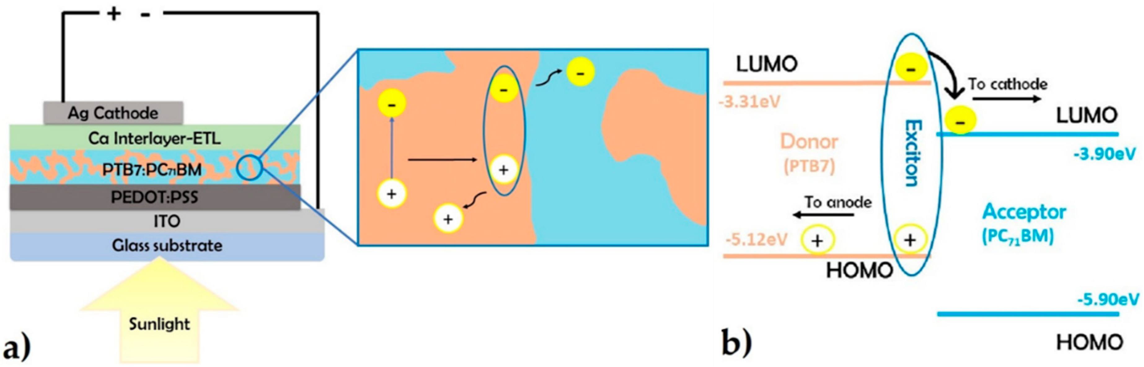
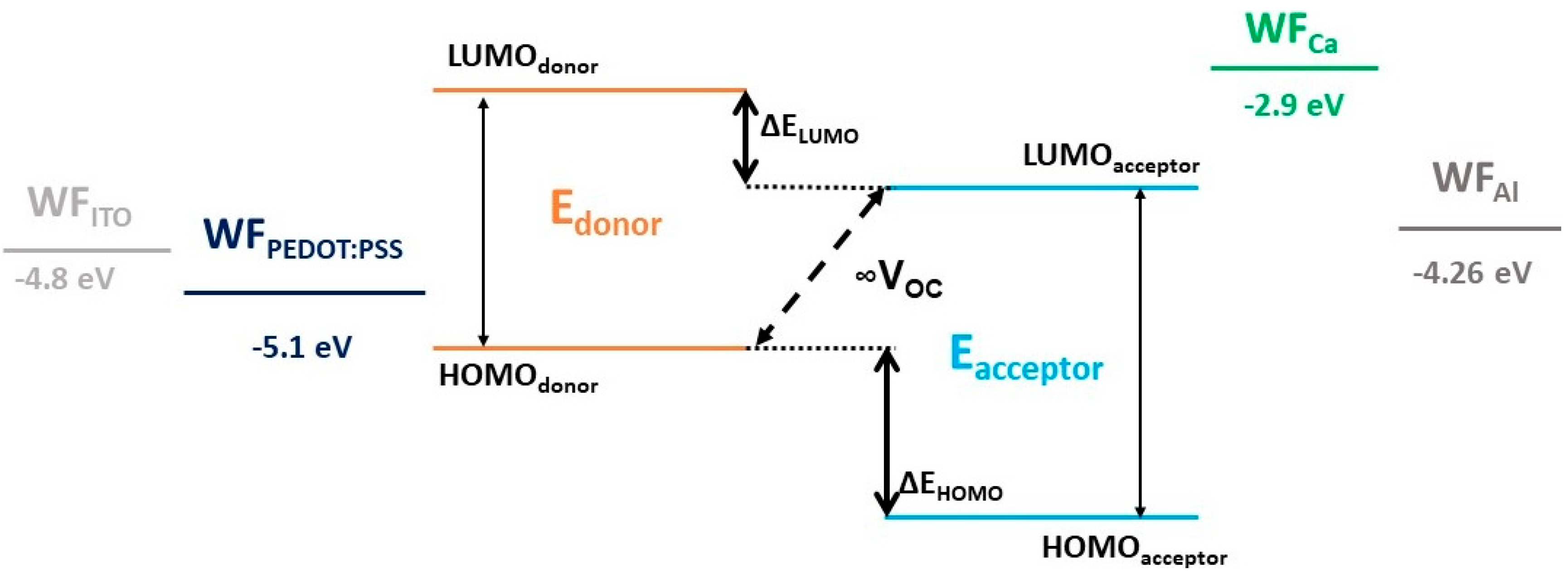
In the conventional configuration of a bulk heterojunction organic solar cell (Figure 1a) [9,10,11,12], a transparent substrate; which can be made of glass and rigid or made of polyethylene terephthalate (PET) and flexible, is coated with a transparent conductor that serves as the anode. The transparent substrate and anode allow light to pass through so that it may be exploited by the photoactive layer. Indium-tin oxide (ITO, In2O3:Sn), a transparent conductive oxide, is one of the most popular employed anode materials due to its transparency and low sheet resistance [12]. In between the anode and the absorbing photo-active layer a hole transport layer (HTL) is placed. This transporting layer operates as an electron blocking layer and at the same time serves as a hole conductor. This dual function lowers a lot the recombination rates and thus enhances the performance of the photovoltaic device [9,13]. Poly(3,4-ethylenedioxythiophene)-poly(styrenesulfonate) (PEDOT:PSS) is one of the most widely used HTL in organic solar cells [14]. In BHJ organic solar cells, the active layer typically consists of a blend of an electron donor and electron acceptor materials [9]. The active layer consists of a mixture of a fullerene derivative e.g., ([6,6]-PhenylC71butyric acid methyl ester, named PC71BM (the electron acceptor) and a conjugated polymer e.g., (Poly[[4,8-bis[(2-ethylhexyl)oxy]benzo[1,2-b: 4,5-b′]dithiophene-2,6-diyl][3-fluoro-2-[(2-ethylhexyl)carbonyl]thieno[3,4-b]thiophenediyl]], named PTB7 (the electron donor).
It is worth mentioning that OSCs based on fullerene-free electron acceptor are also being designed and exhibit advantages compared to the more traditional fullerene-based OSCs. For instance, non-fullerene acceptors have tunable energy band gaps, exhibit low VOC losses due to reduced charge recombination, and are more stable during thermal treatments, and, as a result, higher power conversion efficiencies (PCEs) have been achieved, specifically (13% for single-junction OSCs and >14% for tandem OSCs) [15]. More recently, a PCE of 13.3% was achieved by P. Cheng at al by using two non-fullerene acceptors or NFAs, namely FOIC and F8IC in tandem, these two NFAs have different LUMO levels resulting in a tunable VOC and different energy band gaps resulting in tunable JSC when using them in a blend [16].
In an organic solar cell, photons propagate through the transparent non-absorbing electrode (ITO) and are absorbed by the donor (PTB7 in our case). When a photon is absorbed, an electron is excited from the highest occupied molecular orbital (HOMO) to the lowest unoccupied molecular orbital (LUMO) of the donor, leaving behind a hole (positive charge). The electron and hole form a pair bound by Coulomb forces (in the order of ~0.5 eV for most organic polymers) that migrates as one quasi-particle. The excitons are diffused towards the donor–acceptor interfaces, where they split under the built-in field created by the energy difference between the LUMOs of donor and acceptor materials. This energy difference must be higher that the binding energy of the exciton. The free electrons and holes are generated across the donor–acceptor interface. In order for the excitons dissociate and create these free charge carriers, they need to reach this interface between donor and acceptor. Moreover, due to the low dielectric constant of the majority of the donor materials (and thus strong exciton binding energy), the light-induced excitons have a short lifetime making it crucial that they reach an interface between donor and acceptor within this short lifetime. For this reason, the formed donor/acceptor interfaces should be closer than 10 nm from solar photon absorption point. Once the excitons dissociate at the donor/acceptor interfaces, the free electrons drift through the acceptor material then through the electron transport layer (ETL) and are eventually collected by the cathode. The ETL facilitates the photo-generated electrons in reaching the cathode as fast as possible, at the same time operating as a hole blocking layer prohibiting the holes from reaching the cathode and recombining with the electrons. The collection of free carriers at the respective electrodes results in the generation of an electrical potential difference. Traditional used ETL materials include, among others, Calcium (Ca), TiOx and other metal oxides. Metals such as aluminum (Al), silver (Ag), and gold (Au) are utilized as the cathode materials. In the experiment described in this manuscript Ca is utilized as the ETL and Ag is the selected as the metal cathode. These are the last two materials deposited via thermal vacuum evaporation.
4. Experimental Section
4.1. Safety Precautions
Safety and chemical handling courses were mandatory before the beginning of this experimental session. In this context, suitable personal protective equipment had to be worn at all times during the presented experiment. A lab uniform, protective nitrile gloves, protective goggles, and gas mask were necessary, as well as long trousers and covered shoes. Acetone and IPA are highly flammable solvents, inhalation of these solvents in high concentrations may cause drowsiness, nausea, headaches, and can even result in unconsciousness, and contact with the skin or eyes can cause redness and irritation. Moreover, the parts of the experiments which concerned CB, a toxic and flammable solvent, took place inside a glove box in order to avoid exposure to any fumes, as well as any contact with the skin and eyes. Protective nitrile gloves were put over the glove-box gloves to protect them from any deterioration from CB during the spin-coating process of the active layer. PEDOT:PSS is corrosive to the skin and can cause serious eye damage. PTB7 is not classified as a hazardous or dangerous substance in powder form, however, typical safety measures still apply. PC71BM is highly toxic and thus gas masks were needed additionally to the typical PPE. For further information on the toxicity of each chemical material safety precautions needed, the Materials Safety Data Sheet (MSDS) for each material should be consulted. Hotplates and ovens must be handled with caution as to avoid any possible burns. Students must consider all hazards and safety precautions described above, before entering the laboratory to begin the experimental part.
4.2. Materials and Equipment
All materials and solvents utilized were supplied through commercial sources. The chemical structures/formulas of the compounds used in the organic solar cell devices fabrication are depicted in Table 1.
More specifically, PEDOT:PSS aqueous dispersion with a solid content of 1.3%–1.7% and a PEDOT to PSS ratio of 1:6 was purchased from Heraeus Clevios™. PTB7 and PC71BM were purchased from 1-Materials Inc. (Dorval, QC, Canada) and Solenne BV (Groningen, The Netherlands), respectively. The glass-ITO substrates were purchased from Naranjo Substrates (The Netherlands). These glass substrates are pre-coated by the manufacturer with a transparent ITO layer (thickness of about 100 nm and a surface resistance of ~20 Ω/sq) in a specific pattern which acts as the anode. Deionized water, acetone, and isopropanol were required for the three-step cleaning process of the substrates. Calcium (Ca) and silver (Ag) pellets were used as the ETL and metal cathode respectively and were applied using the thermal vacuum evaporation method.
For the cleaning process of the glass-ITO substrates an ultrasonicator and a UV-Ozone (UV-O3) cleaner were required. A digital multimeter, hot plates with magnetic stirrers, an oven, an analytical balance, and a Gilson pipette were also required throughout the experiment.
For the photovoltaic characterization of the devices and the measurement of HTL hole mobility, the solar light simulator was used. The devices were characterized at room temperature under Air Mass 1.5 Global (A.M. 1.5G). A UV-Vis spectrometer was utilized to obtain the transmittance spectrum of the PEDOT:PSS HTL and the absorption spectrum of the PTB7:PC71BM active layer blend.
4.3. Experimental Procedure—Logistics
4.4. First Day—Session 1
In Session 1, the first three steps of the four-step cleaning process were carried out, so that clean glass-ITO substrates were ready to be used in device fabrication procedures in Session 2. This cleaning process serves to remove any dust particles or contaminating organic matter (e.g., fingermarks) from the ITO surface. The handling of the substrates was done using metal tweezers. The correct area to position the tweezers so as to avoid touching the active area of the device is shown in Figure 3. The PTB7:PC71BM active layer blend was also prepared, as this material must be left stirring on a hotplate before it is ready for use in future sessions.
4.4.1. Four Step Cleaning Process
First step: The substrates were first placed into a specified holder with the ITO-coated side facing in the same direction. To ensure that the ITO side of all substrates was indeed facing on the rightwards or leftwards, a digital multimeter was used to check the conductivity of the surface before the substrates were placed into the holder. The holder was then submerged into a 1000 mL beaker with enough deionized water containing one to two drops of liquid detergent. The deionized water–detergent solute should be just enough to cover the glass-ITO substrates. The beaker was then placed into an ultrasonic bath at room temperature for ten minutes. The ultrasonication cleaning process helps remove all traces of contaminants that have adhered to the ITO surface. The substrates were then thoroughly rinsed with deionized water as to remove all traces of detergent.
Second step: The holder was submerged in acetone in a different 1000 mL beaker for further cleaning and removal of organic residue. The beaker was again put in an ultrasonic bath at room temperature for ten minutes.
Third step: The holder was taken out of the acetone and submerged in isopropanol (2-propanol, IPA) in a 1000 mL beaker which was then put in a last ultrasonic bath at room temperature for ten minutes. The purpose of the isopropanol bath is to remove the acetone of the previous bath which, when dry, would leave marks on the ITO surface. The substrates were then transferred from the holder to a Petri dish with the ITO side facing up. The Petri dish was placed in an oven at 120 °C for at least 15 min for the substrates to dry. The substrates were then be stored in a covered Petri dish at room temperature, ready to be used in Session 2. The fourth step of the cleaning process described below was carried out before the deposition of each film begins.
Fourth step: The fourth and last step of the cleaning process was to place the substrates inside a UV-O3 cleaner chamber (Figure 4) for 15 min at about 1 mW/cm2. This process not only removes any organic contamination, but it also increases the surfaces’ hydrophilicity due to an increase in oxygen concentration, which in turn increases its affinity to the water solved PEDOT:PSS (HTL) which is the next material to be deposited. It has also been shown that UV-O3 treatment of the ITO film planarizes the ITO creating a better interface with the PEDOT:PSS and increases its work function (WF) to 4.7 eV. This increase in the WF of ITO is a desired effect because it assists in better matching with the HOMO energy level of PEDOT:PSS (5.2 eV), the HTL. The better energy-matching will lower the energy barrier the photogenerated holes will experience during their transportation from the HTL onto the anode. It should be pointed out that UV-O3 treatment had to take place a few minutes before the PEDOT:PSS HTL deposition since the increased hydrophilicity effect on the treated ITO-coated substrates is effaced after about 4 h. This treatment was also performed before the fabrication of the hole-only and the electron-only devices began.
4.4.2. Preparation of the Bulk Heterojunction Active Layer Blend
The bulk heterojunction layer which acts as the photoactive layer consists of two materials intimately combined: the electron donor and the electron acceptor materials, which in organic solar cells are usually organic conjugated polymers and fullerene derivatives, respectively. It is essential that the two materials be miscible in the same solvent so that the blend can be successfully prepared.
The donor is the material that absorbs light (photons) and generates excitons. Therefore, it must be a low-energy band gap (Eg) material with high absorbance. A low Eg ensures that more wavelengths of solar light are absorbed. A long exciton diffusion length (LD) is also desired, meaning that the exciton can travel further in the donor material towards its interface with the acceptor and be dissociated. This minimizes exciton recombination losses since it increases the possibility of the exciton meeting the donor–acceptor interfaces where it separates into free carriers: an electron and a hole. The donor should also have a high hole mobility for the holes generated after the exciton dissociation to travel swiftly through the donor towards the active layer/HTL interface without recombining with electrons. In the same sense, the acceptor material should have high electron mobility for the electrons to travel fast toward the active layer/ETL interface avoiding any possible recombination with holes. Moreover, to avoid charge accumulation the HTL and the ETL hole and electron mobilities should be as balanced as possible.
There are many donor and acceptor materials to select from when designing a bulk heterojunction blend. There are a few criteria to follow to find a suitable pair—active layer system. Firstly, it is essential that the energy levels (HOMO and LUMO) of the donor and acceptor align in the manor depicted in Figure 5. The exciton dissociates at the donor/acceptor interfaces due to potential energy difference. The energy difference (ΔELUMO) between the LUMO of the donor and the LUMO of the acceptor must be equal to or larger than the binding energy of the generated exciton (in the most organic donor polymers the exciton binding energy is of the order of 0.3–0.5 eV). That way, when the exciton reaches the donor–acceptor interface, there is a sufficient potential difference (ΔELUMO) for the exciton to dissociate and generate free charge carriers. A lower ΔELUMO value means that the exciton will not dissociate, therefore no free carriers will be generated, however, a larger ΔELUMO compared to the exciton binding energy is considered as a loss and results in a smaller VOC value. It is apparent that the suitable ΔELUMO is a trade-off between the small energy bandgap and the achievement of high VOC value. Note that the VOC value corresponds to the energy difference between the HOMO of the donor and the LUMO of the acceptor (Figure 5).
Table 2 demonstrates a few common donor polymers that are used with the acceptor PC71BM including the LUMO energy values of each donor, the energy difference between the LUMO of each donor and the LUMO of PC71BM (ΔELUMO) as well as the energy bandgap (Eg) of each donor polymer [19]. PC71BM has a LUMO level of 3.9 eV and a HOMO one of 5.9 eV. On the other hand, Table 3 presents a few common organic materials that are used with the donor PTB7 including the LUMO energy values of each acceptor, the energy difference between the LUMO of PTB7 and the LUMO of each acceptor (ΔELUMO), as well as the energy bandgap (Eg) of each [20]. PTB7 has a LUMO level of 3.31 eV and a HOMO one of 5.12 eV.
According to the data presented in Table 2, PTB7 is a suitable donor polymer to be used with PC71BM since the ΔE between the LUMO levels (0.59 eV) is higher than the binding energy of a singlet exciton (0.5 eV). Even though PTB7-Th has a lower band gap energy than PTB7, which as mentioned earlier, is a desired attribute, the ΔELUMO (0.24 eV) is far from 0.5 eV.
When the donor–acceptor pair are selected, the optimization of the bulk heterojunction blend is crucial to the solar device’s performance. Optimization involves achieving a bulk heterojunction structure in which (a) the interfacial area between donor and acceptor is increased and (b) the distance which the exciton must travel to reach the interface is minimized, therefore increasing the possibility of the generated excitons reaching the interface and dissociating. Because the diffusion length of a polymer singlet exciton (LD) is typically 10–20 nm [21], it is also crucial that the excitons are generated at a distance smaller than 10 nm from the donor/acceptor interface to minimize exciton recombination rates. Optimization of the bulk heterojunction blend is achieved through intimate mixing of the two materials to extend the interfacial area, by achieving optimum concentrations and then depositing the blend via spin-coating onto the HTL achieving an ideal thickness. This brings us to the materials used and the experimental parameters followed in this manuscript for the preparation of a suitable BHJ active layer blend.
The donor and acceptor materials utilized in the experiment were the conjugated polymer PTB7 and the fullerene derivative PC71BM, respectively. Their chemical structure can be seen in Table 1. Both these compounds are available in solid powder form and are blended in a mixed solute of chlorobenzene and DIO. A concentration of 25 mg/mL PTB7:PC71BM solution (1:1.5) in chlorobenzene/DIO (97:3 vol%) mixed solvent yields desired results regarding solar device performance and organic solar cells [22]. To prepare the blend, firstly 10 mg of PTB7 were weighed and added to 970 μL of chlorobenzene contained in a 2 mL clear vial. The vial was then placed on a hotplate to be stirred at 70 °C for 60 min. When the hour was up, 15 mg of PC71BM were added to the solution which was stirred overnight at 70 °C. The application of heat and stirring firstly assists in the faster dilution of the PTB7 and PC71BM powder in the CB solute and, secondly, serves to avoid the coagulation that occurs at temperatures lower that 70 °C. While the solution was left to be stirred, it must be kept under dark conditions to minimize light exposure of the material.
4.5. Second Day—Session 2
After being left to be stirred at 70 °C overnight, DIO (30 μL) was added to the mixture and was stirred at 70 °C under dark conditions for 60 min before use [23].
4.5.1. Hole Transport Layer
The hole transport layer (HTL) was deposited between the anode and the active layer in the organic solar cell conventional structure. It serves a dual role in the devices’ operation: Firstly, it transports holes that are generated upon the exciton dissociation to the anode and, secondly, it blocks electrons therefore avoiding carrier recombination. For this reason, the material utilized as the HTL must have high conductivity and high hole mobility to ensure that as many holes as possible are delivered to the anode electrode quickly and efficiently. It is also imperative that the HTL material has a low absorption value; Because light travels through the HTL to reach the active layer, any light absorbed by the HTL material contributes to optical losses and, consequently, to electrical losses for the overall solar cell device. Another variable that effects the optical characteristics of the HTL is the thickness of the film. As mentioned earlier, the absorbance of the HTL must be at a minimum, therefore a small thickness for this layer is desired. However, an HTL that is too thin (less than 10 nm thickness) is inefficient as an electron blocking layer since the electrons may travel through via tunneling effect. There is an optimum thickness for the HTL which balances both low absorbance and efficient electron blocking, and it is experimentally optimized. The ideal thickness of the HTL is a tradeoff between low absorption and efficient electron blocking of this layer. The morphology of the HTL film is also of high importance. The HTL film surface should be as smooth as possible to ensure more pathways for the holes at the active layer/HTL interface. The roughness of a film surface is expressed through the Root Mean Square (RMS) value which can be measured using Atomic Force Microscopy (AFM), as will be addressed in Section 4.5.4.
Poly(3,4-ethylenedioxythiophene) polystyrene sulfonate (PEDOT:PSS), which is a semi-conductive polymer, is a widely used compound as the HTL material in organic solar cells. The chemical structure of this compound is also depicted in Table 1. PEDOT:PSS has a high conductivity value of up to 1000 S/cm and a transparency as high as 90% (for 100 nm thickness) [24], making it a suitable HTL compound.
4.5.2. Deposition of the Hole Transport Layer
The PEDOT:PSS was purchased as a pre-mixed aqueous dispersion with a concentration of 1.3 to 1.7 wt.%. It was stored in a refrigerator for preservation. Before it can be used, it was allowed to reach room temperature in order for its viscosity to be recovered (10–30 cP at 20 °C). The PEDOT:PSS dispersion was deposited via static spin coating. The equipment used can be seen in Figure 6a,b. When it had reached room temperature and was ready to be used, PEDOT:PSS was taken from the vial using a syringe. A 0.45 μm Polyvinylidene Fluoride (PVDF) filter was fixed onto the syringe to remove any impurities or aggregated particles as the PEDOT:PSS was applied. The PEDOT:PSS was applied to the glass-ITO substrate using this syringe-filter set up. Using the settings screen, the spin-coater was set to spin the substrate at 6000 rpm for 60 s [25]. The substrate was then positioned ITO-side up in the center of the rotator. The substrate was held in place via vacuum suction. The PEDOT:PSS was then spread on the substrate with the syringe-filter set up, the lid of the spin coater was closed, and the spin coater was activated. This procedure can be seen performed on a glass-ITO substrate that has undergone UV-O3 treatment and on one that has not in Videos S1 and S2 respectively (provided as supporting material). Students should note that the PEDOT:PSS exhibits better adhesion to the UV-O3 treated substrate, compared to the untreated one, as depicted in Figure 7. This is due to the increase in hydrophilicity of the surface. It is advised that students repeat this process in order to see firsthand the impact of UV-O3 treatment on the quality of the PEDOT:PSS film. When the spin coating procedure was completed, the wiping process was carried out in which a strip of PEDOT:PSS from the top and bottom section of the substrate was wiped away with a cotton swab soaked in deionized water (Video S3). This strip was removed to ensure that the cathode came into contact with the anode (ITO layer) without the HTL blocking it. After this wiping process, the substrates were placed in an oven at 120 °C for 15 min in order to remove the humidity and aid the crystallization of PEDOT:PSS thus forming the HTL film.
4.5.3. Transmittance Measurement of PEDOT:PSS
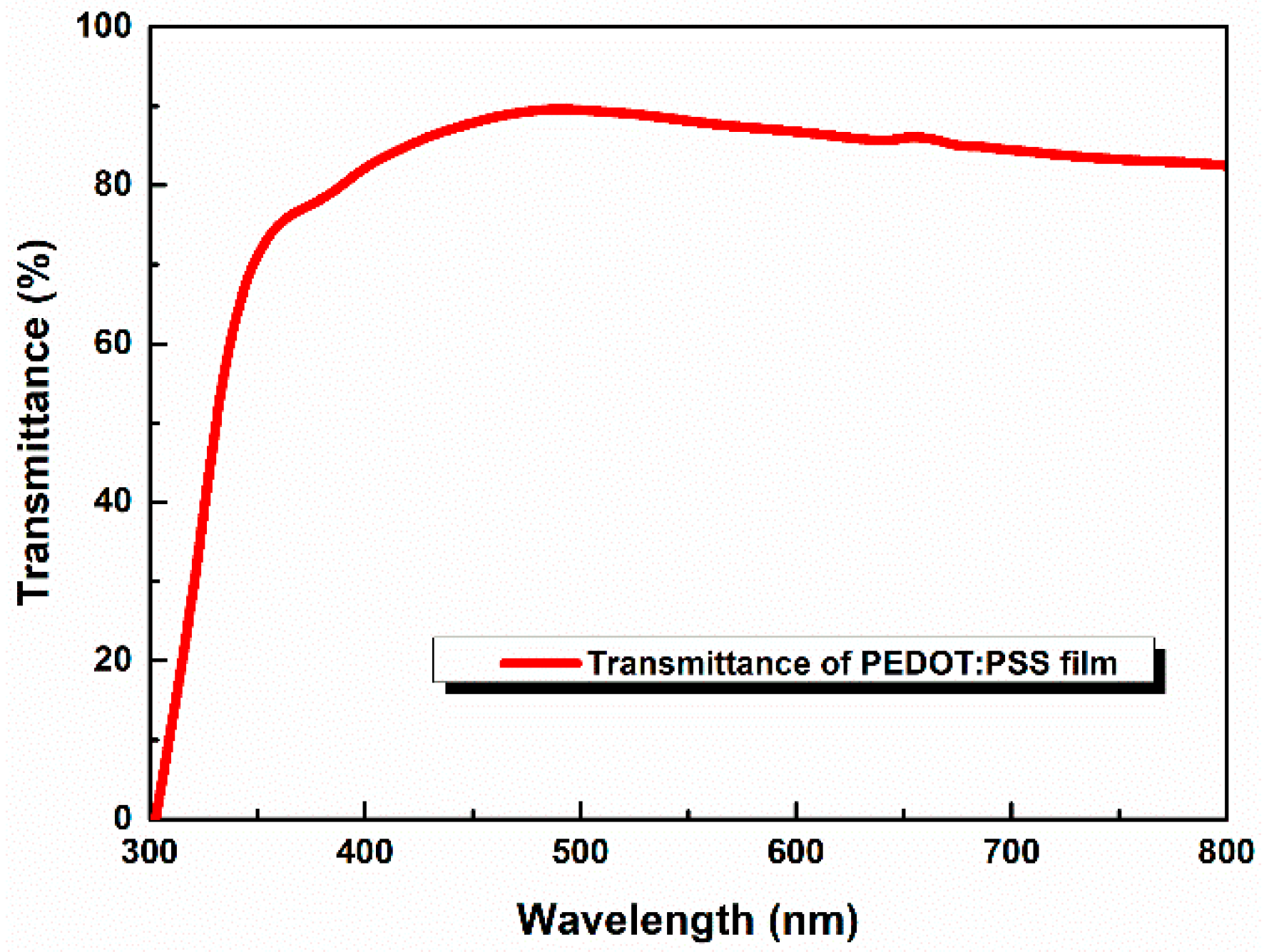
As mentioned earlier, a suitable HTL film should be as transparent as possible. It is of great importance that the material used as the HTL shows very high transmittance in the solar light spectrum, especially in the spectral region where the AL absorbs, ensuring that more light reaches the AL and minimizing optical losses. For this reason, the transmittance of the deposited PEDOT:PSS film was obtained via UV-Vis spectroscopy. A Glass-ITO substrate was used as a reference. Figure 8 depicts the transmittance spectrum obtained for a PEDOT:PSS film deposited at 5000 rpm with a thickness of 25 nm. At wavelengths larger than 389 nm the transparency reaches and surpassed 80% with a maximum transparency value of 88.7% at 462 nm.
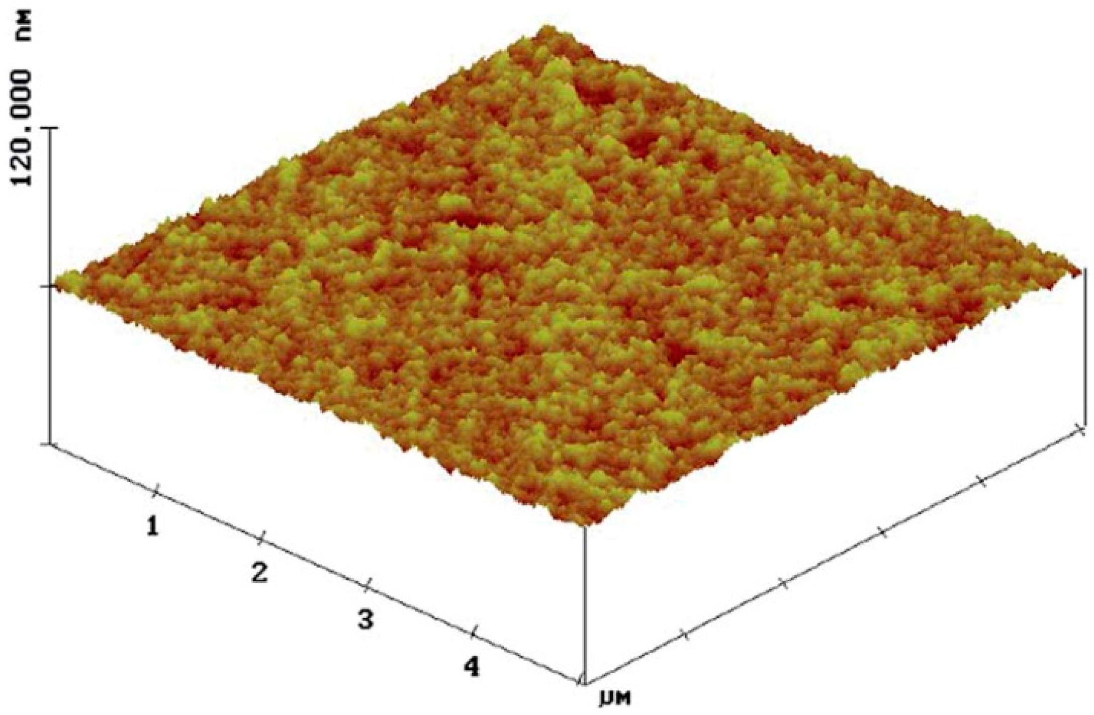
4.5.4. Morphology Characterization of PEDOT:PSS—Atomic Force Microscopy
In solar cell characterization atomic force microscopy (AFM) can be utilized to determine the morphology, the roughness and even the thickness of a film. Performing these measurements on the PEDOT:PSS and the PTB7:PC71BM films gave us insight into how each of the films surface roughness effects the performance of these materials as an HTL and the AL respectively. In this experiment, AFM measurements were performed to assess the surface roughness of the HTL and active layer films by acquiring the root mean square roughness value (RMS) and obtaining an overall view of the surface morphology through 3D imaging. The lower the RMS value, the smoother the film surface is. The roughness of the PEDOT:PSS film is an important parameter in the performance of the cell, as it defines the interface between the HTL and the active layer. A low RMS value indicates a smooth film surface. A smooth HTL film is desired for a better interface, as this results in more available pathways for the generated holes to travel from the donor material into the PEDOT:PSS. It should be noted that the deposition of the AL onto the PEDOT:PSS HTL results in the planarization of the HTL making the surface smoother.
The PEDOT:PSS film that had now been spin coated on the UV-O3 treated glass-ITO substrate and thermally annealed underwent an AFM measurement which gave us information of the film’s morphology, as well as of its roughness. AFM 3D images for PEDOT:PSS films had revealed areas of smaller and larger heights which are represented in the image by light and dark areas respectively. These bright and dark areas are commonly associated with PEDOT and PSS rich regions [25,26]. The low RMS value for the pristine PEDOT:PSS film of 1.124 nm implied its smooth surface (Figure 9).
4.5.5. Sheet Resistance Measurement of PEDOT:PSS
The sheet resistance (Rs) values for the PEDOT:PSS film and, later on, the PTB7:PC71BM active layer film were acquired by firstly obtaining the conductivity data from the Hall-effect measurements using the four-point probe method (Kelvin technique) and performing suitable calculations. Rs affects the way with which charges travel along the surface of a film. Therefore, the Rs value can be an indicator of the efficiency with which charges travel through the PEDOT:PSS and PTB7:PC71BM films and, ultimately, is a factor in the overall performance of the OSC. For these measurements to be conducted, a layer of PEDOT:PSS was spin-coated statically onto a UV-Ozone treated ITO-glass substrate at 5000 rpm for one min and was then annealed in an oven at 120 °C for 15 min. This is in accordance with the parameters followed for the deposition of the PEDOT:PSS layer in the completed solar device. Then, Ag paste was utilized to create electrodes on four corners of the PEDOT:PSS film (four-point probe method). The 4-point probe technique is one of the most common experimental methods for measuring resistivity. This configuration consists of four independent electrical terminals where two terminals are used to apply current to the sample, and the other two terminals measure the resulting potential drop across the defined portion of the sample. In the technique of linear four-point probes all measurement tips are placed along a straight line and separated by a constant distance [28]. The Hall effect measurements were conducted in air, at room temperature. After obtaining the conductivity value (σ) of the PEDOT:PSS film, the Rs value may be calculated using Equations (1) and (2) for a known film thickness.
where ρ is the resistivity, and t is the thickness of the film. The obtained sheet resistance (Rs) value for the PEDOT:PSS film was received using the four-point probe method (Kelvin technique) and determined by Equations (1) and (2) for a film thickness of 25 nm, as confirmed via AFM. For a σ value of 5.086 × 10⁻⁴ S/cm for the PEDOT:PSS film, the ρ value was calculated to be 1.966 × 10³ Ω cm. Therefore, the Rs value for this thickness according to Equation (2) was 7.86 × 10⁷ Ω.
4.5.6. Deposition of PTB7:PC71BM via Dynamic Spin Coating Method
When AFM and UV-Vis measurements had been conducted for the HTL, the deposition of the AL blend followed. The spin coating method for this layer differed from that used for the HTL. Firstly, it took place inside the controlled inert conditions of a glove box (N2 gas). Secondly, the active layer was applied using the dynamic spin-coating method. This method is different than that of the static spin coating procedure, in that the substrate is first set into rotation and then the blend is deposited while the substrate is spinning.
Using the settings screen, the spin coater was set to spin the substrates at 2500 rpm for 30 s. It has been reported that these parameters result in the optimum thickness of the BHJ blend. In our case this thickness has been shown to be about 85 nm, improving the tradeoff between photon absorption and minimum distance the exciton must travel to reach the donor/acceptor interfaces. For the deposition of the active layer blend the substrate is placed in the slot and 50 μL of the solution are acquired with a Gilson pipette. The substrate was then set into rotation and the blend was applied (dynamic mode). After the active layer had been deposited, the substrates were placed in an active vacuum for 20 min to remove the CB solute. A strip from the top and bottom of each substrate was then wiped with a cotton swab soaked in anhydrous CF, ensuring that the ITO anode and Ag cathode would come into contact when the device is complete. It should be noted that during this procedure the gloves of the glove box were covered by a pair of disposable nitrile gloves, to protect them from any damage that may be caused by organic solvents such as CF.
4.5.7. Absorption Measurement of PTB7:PC71BM via UV-Vis Spectroscopy
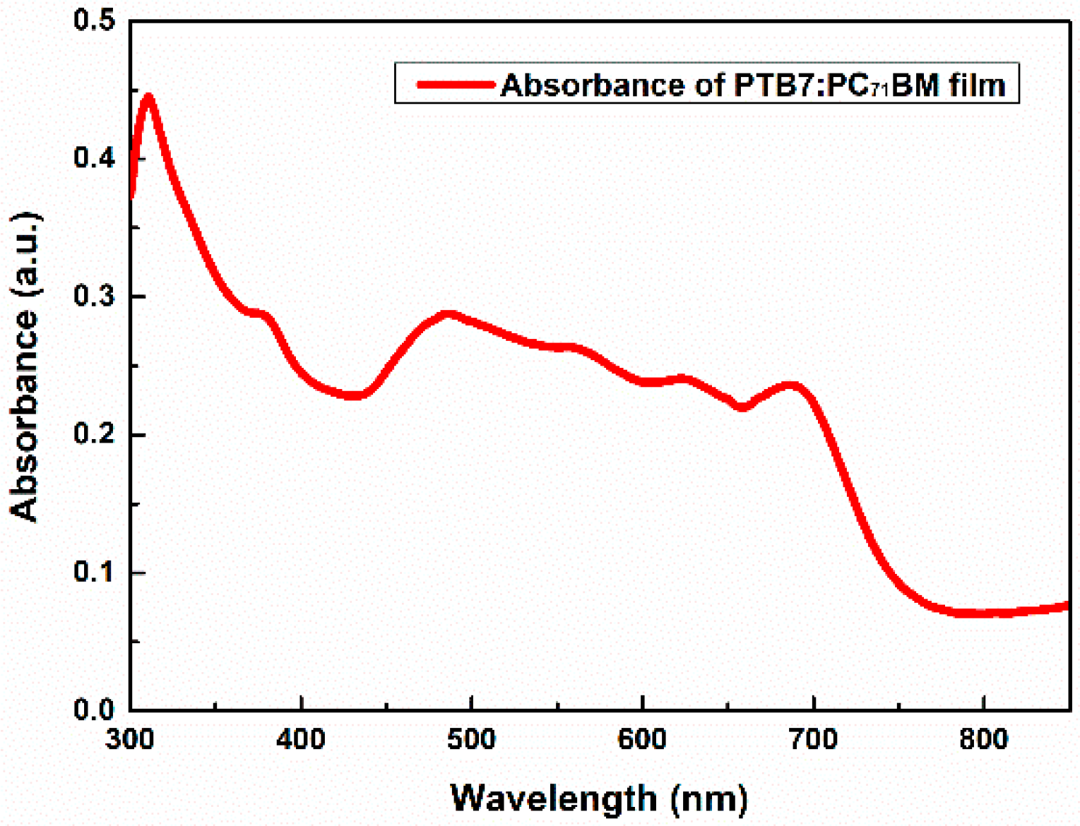
The absorption spectrum of the AL film was obtained via UV-Vis spectroscopy. It was possible to measure the absorption of the donor and acceptor material separately. As mentioned earlier, the donor material is the component that absorbs photons and generates excitons. Therefore, it is important that the donor material has high absorption intensity and a wide absorption spectrum. The absorption spectrum for the active layer blend was obtained using a UV-Vis Spectrometer, where a glass/ITO/PEDOT:PSS structure was the reference device. This technique provides a way of investigating how efficiently this active layer blend absorbs in the Ultra Violet and Visible region of the sunlight spectrum.
The respective UV-vis spectrum for PTB7:PC71BM blend can be seen in Figure 10. This polymer-fullerene blend exhibits the strongest absorption in the visible region and extends into the near infrared region (NIR) with lower absorption values. Maximum absorption was measured at 307 nm. The maximum absorption observed in the visible was at 506 nm. It should be noted that is desirable for the HTL materials to demonstrate very low absorption at the visible region. This decreases the optical losses as more photons surpass the HTL and are absorbed by the donor in the AL. However, with minimal HTL light absorption, as will be discussed below, the completed device was fully operating and showed moderate efficiency. For higher device performance, the HTL film should ideally be fully transparent or at least where the active layer absorbs light (normal structured devices).
4.5.8. Morphology Characterization of PTB7:PC71BM—Atomic Force Microscopy
After the deposition of the AL, AFM measurements were also conducted on this film mainly to determine its roughness. The roughness of the AL surface is an important parameter for the device’s performance. As with the case of PEDOT:PSS, a smoother film surface ensures a smoother interface with the next material to be deposited. A smoother AL surface ensures a better interface between the AL and the ETL resulting in more efficient extraction of electrons from the electron donor to the ETL. The increase in charge extraction contributes to better charge collection, therefore increasing the FF value and, by extent, the PCE value. Furthermore, the more efficient electron extraction owing to an optimized interface results in less charge recombination therefore in a larger free carrier number. This has a positive effect on the JSC value.
The morphology of the AL film was evaluated by determining the roughness via AFM. An indicative surface image obtained via AFM measurement for PTB7:PC71BM deposited on PEDOT:PSS can be seen in Figure 11 for which the RMS value was 1.099 nm.
4.5.9. Sheet Resistance Measurement of PTB7:PC71BM
The same method applies as with the Rs measurement of PEDOT:PSS. First, a layer of PTB7:PC71BM was deposited onto an UV-O3 treated glass-ITO substrate according to the spin coating parameters of the active layer for the completed device; 50 μL of PTB7:PC71BM were dynamically spin coated onto the substrate at 2500 rpm for 30 s in the inert conditions of a glovebox. The substrate was then placed in an active vacuum chamber for 20 min and Ag paste was used to create four points on the PTB7:PC71BM film to serve the purpose of electrodes for the Hall effect measurement.
As with PEDOT:PSS the Rs value for the PTB7:PC71BM active layer film was obtained using the four-point probe method and determined by Equations (1) and (2) (Section 4.5.5) for a film thickness of 85 nm which was confirmed by AFM. Taking into account the conductivity value of 1.2 × 10⁻⁶ S/cm and using Equations (1) and (2), a sheet resistance value of 7.24 × 10¹⁰ Ω was calculated.
4.5.10. Deposition of the Ca—ETL and the Ag cathode
The calcium and silver layers were deposited via vacuum thermal evaporation (VTE). The thermal vacuum evaporator was located inside a glove box ensuring that atmosphere sensitive materials remain stable. In this process, Ca and Ag pellets were placed in a cavity enclosed within a vacuum chamber. The metal that was to become the coating was placed on a specified base, which was known as a “boat”, over the cavity. Separate boats are used for Ca and Ag. The cavity was supplied with a current of 165.1 A for Ca and 146.7 A for Ag and, due to its Ohmic resistance, was heated under vacuum conditions of 10−6 mbar. The metal pellets melt and evaporate. The vaporized molecules of the material overlaid on the substrate and formed the coating. The coating thickness depends on the distance of the substrate from the cavity (source evaporation) and the time of supply with electricity. The overlay can be made on specific parts of the substrate with the use of shadow masks. This mask left only the area we wished to coat exposed. Firstly, 5 nm of Ca were deposited onto the substrates. Then 100 nm of Ag were evaporated to form the cathode.
Ag has a work function of −4.26 eV whereas the ITO anode has a work function of −4.8 eV. This way the free charges generated in the active layer drift toward the respective electrodes, due to a difference in potential. The free electrons and holes are driven by built-in electric field and are collected by the electrodes thus generating electric current.
4.5.11. Carrier Mobility: Hole Mobility—Electron Mobility
The last characterization method to be performed was the measurement of hole and electron mobility of the acceptor and the donor respectively. Carrier mobility in a semiconductor is one of the most important parameters for the operation of electronic devices, organic solar cells included. The mobility measures the ability of free carriers (electrons or holes) to move in the material as it is subjected to an external electric field. Hole or electron mobility is essentially the ability of a hole or electron to move through a metal or semiconductor when electrical charge is applied.
The hole mobility of each fabricated device can be calculated using the Mott–Gurney equation (Equation (3)) below:
where μ is the hole mobility value, ε0 is vacuum permittivity with a value of ε0 = 8.854 × 10⁻¹² F/m, εr is the relative permittivity, which for organic solar cells has a value of εr = 3 and L is the thickness of the PEDOT:PSS layer. V was the measured electric potential and Vbi is the built-in potential, which for PEDOT:PSS has a value of Vbi = 0.3 V.
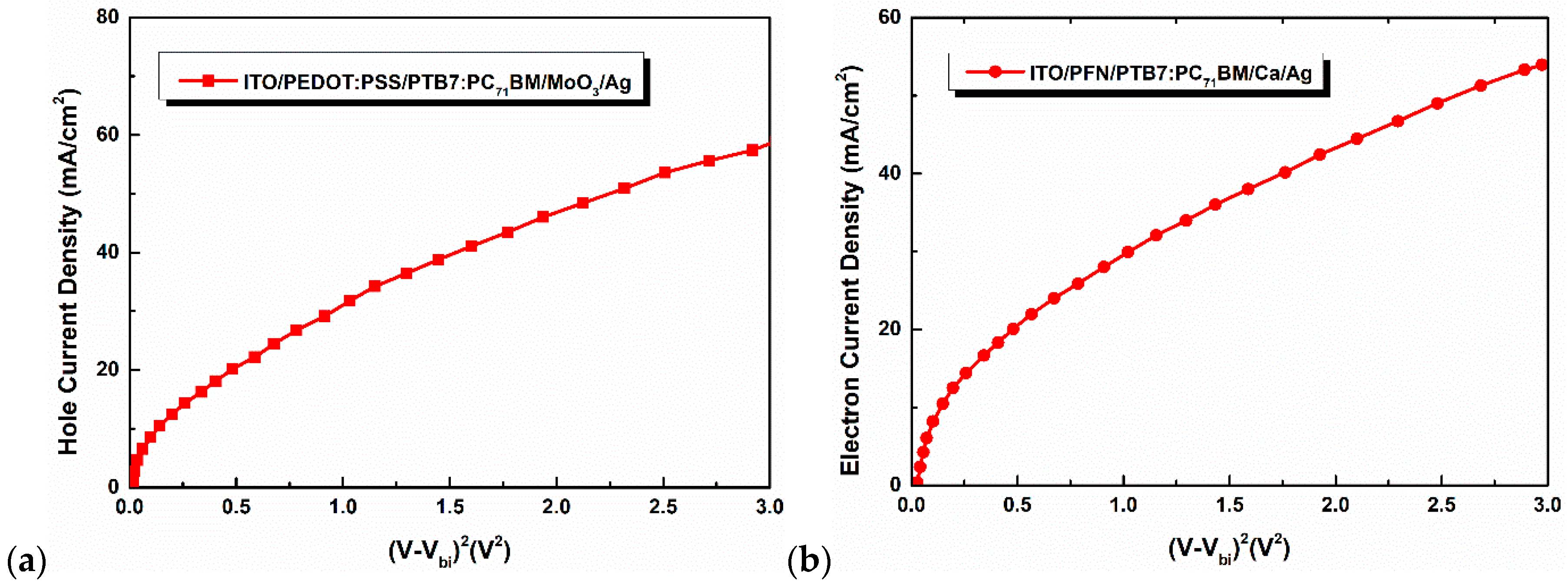
To measure the hole mobility, a “hole only” transport device was fabricated. This device differs from the initial fabricated device in that the ETL is replaced by an HTL; namely the Ca ETL is replaced with an MoO3 interlayer that acts as an HTL. So, a device with the following structure was fabricated: Glass/ITO/PEDOT:PSS/PTB7:PC71BM/MoO3/Ag, where the MoO3 layer is deposited via thermal vacuum evaporation with a final thickness of 8 nm. The hole-only device was fabricated following the same parameters previously mentioned for the fabrication of the fully operational BHJ OSC. More specifically PEDOT:PSS was spin coated statically at 5000 rpm, 50 μL of PTB7:PC71BM was dynamically spin coated at 2500 rpm for 30 s, 8 nm of MoO3 were deposited instead of 5 nm of Ca, and lastly 100 nm of Ag were deposited via thermal vacuum deposition. The J-(V-Vbi)2 graph was then obtained for this device using a solar simulator. Figure 12a shows a graph for a Glass/ITO/PEDOT: PSS/PTB7:PC71BM/MoO3/Ag, device. The hole mobility value was calculated as follows: The value of the fitting slope in a J-(V-Vbi)2 graph is equal to the JSC value in the Mott–Gurney equation (Equation (3)). Therefore, by substituting this value and solving for μ the hole mobility value for the PEDOT:PSS layer can be calculated. The μh value calculated for this device was 5.81 × 10⁻⁴ cm2 V−1 s−1.
Similarly, for the electron mobility measurement an “electron only” transport device was fabricated. This device has a structure of: glass/ITO/PFN/PTB7:PC71BM/Ca/Ag, where PFN is the conjugated organic polymer Poly [(9,9-bis(3′-(N,N-dimethylamino)propyl)-2,7-fluorene)-alt-2,7-(9,9–dioctylfluorene)]. A PFN solution with a concentration of 0.4 mg/mL in a solute consisting of 98 μL of deionized water and 2 μL acetic acid was prepared in the inert conditions of a glove box. Four layers of PFN were deposited onto the ITO anode via dynamic spin coating at 1000 rpm inside a glove box. The rest of the fabrication process for this device was identical to the fabrication process of the conventional bulk heterojunction organic solar cell described in this manuscript. The J-(V-Vbi)2 graph was then obtained for this device using a solar simulator and the electron mobility value (μe) was calculated using the Mott–Gurney equation, as done previously in the case of hole mobility (μh). An electron current density-(V-Vbi)2 graph obtained for an electron only device can be seen in Figure 12b, for which the μe value was calculated to be 6.01 × 10⁻⁵ cm2 V−1 s−1.
The μh/μe can be a good performance indicator for the solar device; ideally, the μh/μe ratio should be approaching the unity in order to reduce the charge accumulation effect in the interfaces; thus, reducing the recombination rates. This would mean that all the free electron and free holes generated would successfully travel at the same velocity within the ETL and HTL respectively and be collected by the respective electrodes. In practice, however, this ideal condition has never been achieved, so a small μh/μe ratio is the goal when designing an organic solar cell; in our case, the μh/μe ratio was 9.67.
5. Device Characterization
5.1. Third Day—Session 3
5.1.1. Electrical Performance—Organic Solar Cell Device Evaluation—Photovoltaic Performance
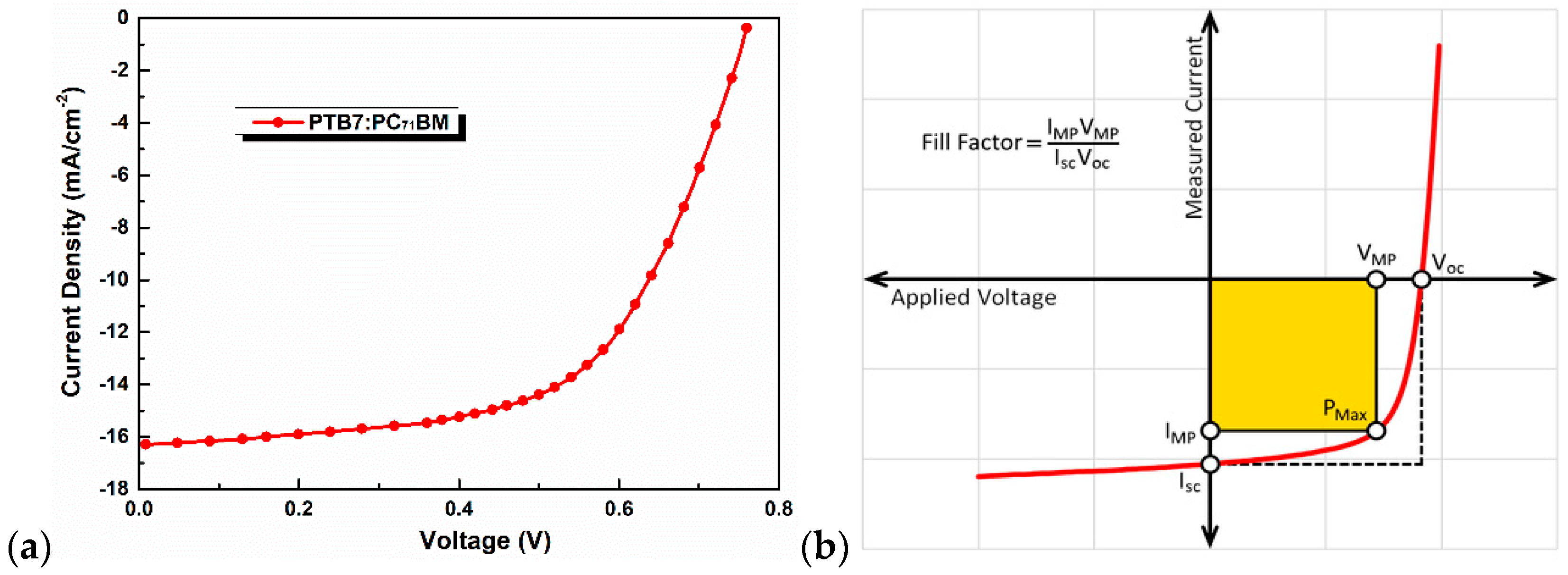
The photovoltaic performance of the device was evaluated by measuring the current density versus voltage (J–V) under conditions of light using a solar light simulator and obtaining the photovoltaic parameters, short current density (JSC), the open circuit voltage (VOC), the power conversion efficiency (PCE), and the fill factor (FF). A J–V curve obtained for a photovoltaic device fabricated following the parameters described in this manuscript can be seen in Figure 13a.
The open circuit voltage (VOC) is the maximum voltage provided by the solar cell and occurs under open circuit mode. The VOC should be representative of the difference between the work function (WF) values of the electrodes. A device with an ITO anode (WFITO = 4.7–4.9 eV) and an Ag cathode (WFAg = 4.2 eV) should yield, in theory, a VOC of 0.5–0.7 eV. However, VOC values are analogous in practice with a typical value linearly dependent on the energy difference between the EHOMO of the donor material and the ELUMO of the acceptor material (Figure 5).
The circuit generated from the solar device is equal to the number of photoinduced carriers that are eventually collected at the electrodes. Therefore, it is dependent on the photon absorption efficiency of the active layer, the exciton dissociation efficiency and the free carrier collection efficiency.
The “Fill Factor”, more commonly known by its abbreviation “FF”, is a parameter which, in conjunction with VOC and JSC, determines the maximum power from a solar cell. The FF is defined as the ratio of the maximum power from the solar cell to the product of VOC and JSC. The FF value can be derived from the J–V measurement and is given from Equation (4) below, where Pmax is the maximum power, PT is the theoretical power that would be output at both the open circuit voltage and short circuit current together, JMP is the current density for maximum power, VMP is the voltage for maximum power. The FF is representative of the overall performance of the solar cell, considering the efficiency of charge generation in the donor material, charge separation at the donor–acceptor interface and charge collection at the electrodes.
Graphically, the FF is the area of the largest rectangle in which J–V curve can be contained which is illustrated in Figure 13b.
The main performance indicator is the power conversion efficiency (PCE or η), under standard reporting conditions (SRC) (temperature, spectral irradiance, and total irradiance) and it is equal to the maximum electrical power divided by the total incident irradiance (Pin = 1000 W/m2, AM 1.5). The PCE value is given by Equation (5) below and is representative of the overall functionality of a solar cell.
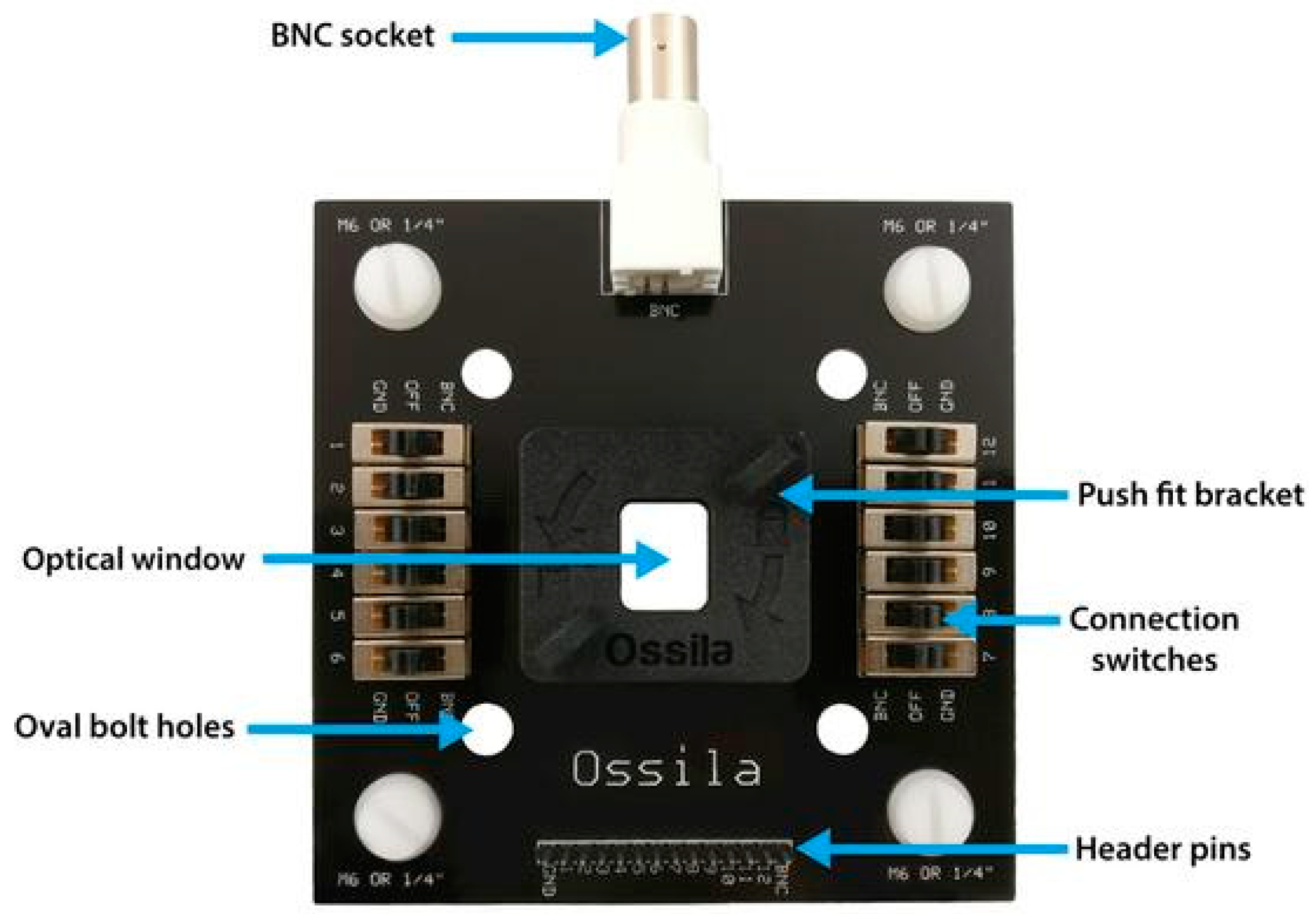
A computer-controlled voltage and current sources provided the voltage difference and the current across the device. First, the lamp was turned on and the power was set to one Sun level (100 mW/cm2). The device was placed into the characterization set-up and the necessary wiring followed. Initially, we brought together two metal probes of the Ossila test board, shown in Figure 14. The whole layout was covered with a black box in order to start the measurement process under dark conditions. The Easy Expert software was launched, purchased from Keysight Technologies, solar cell mode was selected, the range and voltage were set, and finally the corresponding current–voltage curve was obtained in the dark. The algorithm of the program calculates important values for solar cells like short circuit current density (JSC, mA/cm2), open circuit voltage (VOC, V), power maximum (Pmax, W), fill factor (FF), power conversion efficiency (PCE, %).
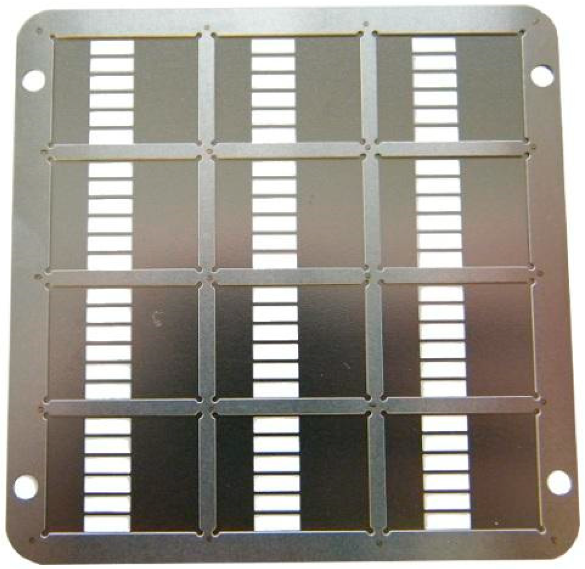
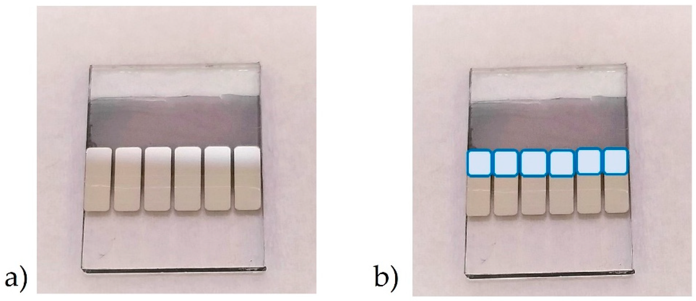
The shadow mask used for the device patterning during Ag deposition via vacuum thermal evaporation (VTE) is shown in Figure 15. The complete fabricated BHJ OSC device is shown in Figure 16a, where Ag was used as the cathode (silver area). The blue squares superimposed onto the photograph indicate the active area of the device (Figure 16b). The active area is that in which all layers of the OSC are present, starting from the ITO anode and ending at the Ag cathode. This is the area in which photocurrent is generated.
Low JSC, VOC, and FF values can be attributed to optical and electrical losses. Optical losses occur through inefficient exciton generation through photon absorption, while electrical losses are attributed to poor free charge generation and collection. There are several loss mechanisms that may take place throughout at every stage of an OSC’s operation cycle. Firstly, there exist surface reflection losses. Not all photons from incident light are absorbed, as part of the beam is reflected. The reflective light is no longer available for the generation of electron–hole pairs within the device. The layers that proceed the active layer within the OSC structure, namely the ITO anode and the PEDOT:PSS HTL, inevitably absorb a number of the photons that do enter the device. ITO being an extremely transparent material does not significantly contribute to this phenomenon. PEDOT:PSS, on the other hand, does not show low transmittance vales at wavelengths lower than 389 nm as seen in Figure 8, meaning that some photons are absorbed by PEDOT:PSS thus never reaching the photoactive layer in order to generate excitons. Losses occur within the active layer for several reasons. For instance, not all wavelengths are absorbed with the same intensity by the donor–acceptor blend, as seen in Figure 10. PTB7:PC71BM shows lower absorbance intensity in some regions of the visible spectrum, meaning that photons with the “wrong” wavelength are not absorbed by the donor to generate excitons. This is the reason that, ideally, the active layer should have a broad absorption spectrum with high absorbance at all wavelengths. A loss that also occurs in the active layer is that caused by charge recombination. Once excitons are generated in the donor polymer, a number of them may recombine, meaning that the electron recombines with the hole and the exciton no longer exists. This takes place when the distance between the exciton generation site and the donor–acceptor interface is larger than the exciton diffusion length (LD). The result is less free charge carrier generation which leads to electrical losses. Electrical performance is also affected by the sheet resistance (Rs) of the individual layers. The lower the Rs, the easier the free charge carriers flow toward the respective electrodes, however, Rs can never practically be zero leading to diminished JSC.
A factor in the lowered performance of the cell may also be PTB7’s low stability in ambient air. To combat this, the fabrication process from the active layer deposition onward should be carried out in the inert conditions of a glovebox. Alternatively, a different polymer with higher stability in ambient air, such as PTB7-Th, can be used as the electron donor instead.
5.1.2. External Quantum Efficiency
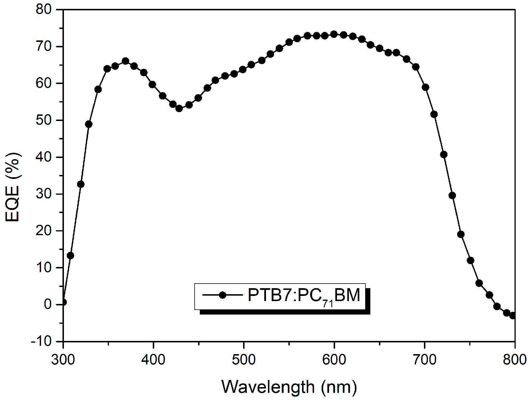
The external quantum efficiency (EQE) measurements were taken in order to cross check the measurements taken during the J–V characterization. Quantum efficiency (QE) is a measure of how efficiently the device converts the incident light into electrical energy at a given wavelength. EQE is the ratio between the number of collected carriers and the number of all the incident photons on the device active area at a given wavelength. The principle of EQE measurement is based on illuminating the sample by a monochromatic light and recording the device electrical current (number of generated carriers). By varying the frequency of the light, the entire curve of the current as a function of wavelength can then be established. The area under the curve will then represent the total number of carriers created by the device under full spectrum white light illumination. In other words, the integration of the curve will give the electrical current density. An EQE curve for a PTB7:PC71BM blend is shown in Figure 17.
Before the solar device could be removed from the glovebox, it needed to be protected from the oxygen and moisture present in ambient atmosphere which cause degradation to all the materials that the solar device consists. The calcium used as the ETL showed significant degradation over a short period of time. Protection from ambient atmosphere was achieved by encapsulation in which a glass was applied to the active area of the device and held in place with a light-curable encapsulation epoxy which acted as an adhesive. More specifically 100 μL drops of epoxy were applied to the surface of a 12 mm × 15 mm piece of glass, ensuring that the epoxy was spread evenly over the glass surface. This epoxy covered glass was then applied to the device epoxy-side down covering the Ag electrodes and, by extent, the active area. The device was then placed in a UV lamp for 30 min to treat and dry the epoxy glue. The device could then be transferred from the glovebox into ambient atmosphere and used for EQE measurement. The JSC value obtained from the EQE measurement for the fabricated device was 15.81 mA/cm2.
Also observed in the EQE curve is the contribution of PC71BM to the generated photocurrent. This is evident from the peak observed between 360 nm and 380 nm. This shows that light absorption and charge generation i.e., exciton formation does not take place only in the electron donor polymer, but also in the fullerene-based electron acceptor [30,31].
An essential reason for measuring the EQE of a bulk heterojunction organic solar cell is to obtain the JSC value from the EQE graph and compare it to the JSC value obtained from the J–V graph. Essentially, the measurement of the EQE is a method of verification of the JSC and VOC values measured via solar simulator. Ideally, the JSC(EQE), also called integrated JSC (JSC,int), should be equal to the JSC(J–V), however, in practice this is never the case. Therefore, it is generally accepted that the deviation of the JSC(EQE) from the JSC(J–V) should be no more than 3%.
Figure 13a depicts the experimental J–V curves of the photovoltaic device based on PTB7:PC71BM AL under illumination of 100 mW/cm2. All photovoltaic parameters (JSC, VOC, and FF) were calculated, while the PCE value was determined by Equation (5), as displayed in Table 4. Finally, the JSC value obtained from the EQE measurement for the fabricated device was 15.81 mA/cm2, whereas the JSC value obtained from the J–V curve was JSC(J–V) = 16.32 mA/cm2. This means that the EQE calculated JSC value was less than 3% different than the actual measured JSC values, indicating good accuracy of the electrical organic solar cell measurement.
6. Conclusions
To sum up, students paid close attention during the whole experimental procedure and made their notes regarding the substrates’ cleaning and solutions preparation processes (1st day), as well as the device fabrication step-by-step (2nd day) and characterization (3rd day). Each layer of the device was characterized upon its deposition. In this context, the HTL and the AL, the “heart” of the device, were characterized through spectroscopic, electrical, and morphological characterization techniques.
The present manuscript offers insight on the operating principles of a bulk heterojunction organic solar cell, presents a full description of the fabrication procedure followed in the construction of said photovoltaic device, as well as several fundamental photovoltaic device characterization techniques. Preceding the description of each step, its importance and the physical meaning were explained. The role and the selection criteria of each material used were analyzed. Therefore, it serves as an elementary guide for the teaching of these fabrication and characterization processes to undergraduate students. Not only did the students gain insight into the solar device fabrication process, they also became familiar with the basic laboratory methods utilized during this process. Furthermore, they better understood the fundamentals of operation of an organic photovoltaic cell and, by extension, photovoltaic cells in general, as well as which material properties must be enhanced through treatments and functionalization in order to improve the efficiency of a photovoltaic cell.
Supplementary Materials
The following are available online at https://www.mdpi.com/1996-1073/12/11/2188/s1, Video S1: Spin Coating of UV-O3 Treated, Video S2: Spin Coating of Non-UV-O3 Treated, Video S3: Wiping Process.
Author Contributions
Conceptualization, M.M.S. and K.P.; Methodology, K.A., M.M.S., and K.P.; Formal Analysis, K.A., M.M.S., and K.P.; Investigation, K.A., M.M.S., and K.P.; Data Curation, K.A. and M.M.S.; Writing—Original Draft Preparation, K.A. and M.M.S.; Writing—Review and Editing, K.A., M.M.S., and K.P.; Supervision, E.K.; Project Administration, M.M.S. and K.P.; Funding Acquisition, M.M.S. and K.P.
Funding
This research was co-funded by the Erasmus+ Capacity Building Project entitled “Innovative Photonic Education in Nanotechnology—iPEN” of the European Union with project number 586165-EPP-1-2017-1-EL-EPPKA2-CBHE-JP.
Acknowledgments
The authors would like to thank Miron Krassas for assisting in the making of the video footage provided as supporting materials.
Conflicts of Interest
The authors declare no conflicts of interest.
References
- Mickey, C.D. Solar photovoltaic cells. J. Chem. Educ. 1981, 58, 418. [Google Scholar] [CrossRef]
- Abruña, H.D. Energy in the Age of Sustainability. J. Chem. Educ. 2013, 90, 1411–1413. [Google Scholar] [CrossRef]
- Liu, X.; Zhang, C.; Duan, C.; Li, M.; Hu, Z.; Wang, J.; Liu, F.; Li, N.; Brabec, C.J.; Janssen, R.A.J.; et al. Morphology Optimization via Side Chain Engineering Enables All-Polymer Solar Cells with Excellent Fill Factor and Stability. J. Am. Chem. Soc. 2018, 140, 8934–8943. [Google Scholar] [CrossRef] [Green Version]
- Smestad, G.P.; Grätzel, M. Demonstrating Electron Transfer and Nanotechnology: A Natural Dye-Sensitized Nanocrystalline Energy Converter. J. Chem. Educ. 1998, 75, 752. [Google Scholar] [CrossRef]
- Dubey, A.; Adhikari, N.; Mabrouk, S.; Wu, F.; Chen, K.; Yang, S.; Qiao, Q. Strategic Review on Processing Routes towards Highly Efficient Perovskite Solar Cells. J. Mater. Chem. A 2018, 6, 2406–2431. [Google Scholar] [CrossRef]
- Li, F.; Liu, M. Recent efficient strategies for improving the moisture stability of perovskite solar cells. J. Mater. Chem. A 2017, 5, 15447–15459. [Google Scholar] [CrossRef]
- Lu, L.; Zheng, T.; Wu, Q.; Schneider, M.A.; Zhao, D.; Yu, L. Recent Advances in Bulk Heterojunction Polymer Solar Cells. Chem. Rev. 2015, 115, 12666–12731. [Google Scholar] [CrossRef]
- Cherrette, V.L.; Hutcherson, C.J.; Barnett, J.L.; So, M.C. Fabrication and Characterization of Perovskite Solar Cells: An Integrated Laboratory Experience. J. Chem. Educ. 2018, 95, 631–635. [Google Scholar] [CrossRef]
- Renny, A.; Yang, C.; Anthony, R.; Lunt, R.R. Luminescent Solar Concentrator Paintings: Connecting Art and Energy. J. Chem. Educ. 2018, 95, 1161–1166. [Google Scholar] [CrossRef]
- Lai, T.H.; Tsang, S.W.; Manders, J.R.; Chen, S.; So, F. Properties of interlayer for organic photovoltaics. Mater. Today 2013, 16, 424–432. [Google Scholar] [CrossRef]
- Leo, K. Organic photovoltaics. Nat. Rev. Mater. 2016, 1, 16056. [Google Scholar] [CrossRef]
- Marinova, N.; Valero, S.; Delgado, J.L. Organic and perovskite solar cells: Working principles, materials and interfaces. J. Colloid Interface Sci. 2017, 488, 373–389. [Google Scholar] [CrossRef]
- Lattante, S. Electron and hole transport layers: Their use in inverted bulk heterojunction polymer solar cells. Electronics 2014, 3, 132–164. [Google Scholar] [CrossRef]
- Seo, J.H.; Koo, J.R.; Lee, S.J.; Seo, B.M.; Kim, Y.K. Efficient Organic Photovoltaic Devices by Using PEDOT:PSS with Excellent Hole Extraction Ability. J. Nanosci. Nanotechnol. 2011, 11, 7307–7310. [Google Scholar] [CrossRef]
- Cheng, P.; Li, G.; Zhan, X.; Yang, Y. Next-generation organic photovoltaics based on non-fullerene acceptors. Nat. Photonics 2018, 12, 131–142. [Google Scholar] [CrossRef]
- Cheng, P.; Liu, Y.; Chang, S.-Y.; Li, T.; Sun, P.; Wang, R.; Cheng, H.-W.; Huang, T.; Meng, L.; Nuryyeva, S.; et al. Efficient Tandem Organic Photovoltaics with Tunable Rear Sub-cells. Joule 2019, 3, 432–442. [Google Scholar] [CrossRef]
- Stylianakis, M.M.; Konios, D.; Viskadouros, G.; Vernardou, D.; Katsarakis, N.; Koudoumas, E.; Anastasiadis, S.H.; Stratakis, E.; Kymakis, E. Ternary organic solar cells incorporating zinc phthalocyanine with improved performance exceeding 8.5%. Dyes Pigments 2017, 146, 408–413. [Google Scholar] [CrossRef]
- Kakavelakis, G.; Del Rio Castillo, A.E.; Pellegrini, V.; Ansaldo, A.; Tzourmpakis, P.; Brescia, R.; Prato, M.; Stratakis, E.; Kymakis, E.; Bonaccorso, F. Size-Tuning of WSe2 Flakes for High Efficiency Inverted Organic Solar Cells. ACS Nano 2017, 11, 3517–3531. [Google Scholar] [CrossRef]
- Sigma-Aldrich—P3HT—Poly(3-hexylthiophene-2,5-diyl) Regioregular, Electronic Grade, 99.995% Trace Metals Basis, Average Mn 30,000–60,000. Available online: http://www.sigmaaldrich.com/ (accessed on 23 April 2019).
- He, Z.; Zhong, Z.; Su, S.; Xu, M.; Wu, H.; Yong, C. Enhanced power-conversion efficiency in polymer solar cells using an inverted device structure. Nat. Photonics 2012, 6, 591–595. [Google Scholar] [CrossRef]
- Benten, H.; Mori, D.; Ohkita, H.; Ito, S. Recent research progress of polymer donor/polymer acceptor blend solar cells. J. Mater. Chem. A 2016, 4, 5340–5365. [Google Scholar] [CrossRef] [Green Version]
- To, C.H.; Ng, A.; Dong, Q.; Djurisič, A.B.; Zapien, J.A.; Chan, W.K.; Surya, C. Effect of PTB7 Properties on the Performance of PTB7:PC71BM Solar Cells. ACS Appl. Mater. Interfaces 2015, 7, 13198–13207. [Google Scholar] [CrossRef] [PubMed]
- Huang, D.; Li, Y.; Xu, Z.; Zhao, S.; Zhao, L.; Zhao, J. Enhanced performance and morphological evolution of PTB7: PC71BM polymer solar cells by using solvent mixtures with different additives. Phys. Chem. Chem. Phys. 2015, 17, 8053–8060. [Google Scholar] [CrossRef] [PubMed]
- Heraeus—Conductive Polymers. Available online: https://www.heraeus.com/ (accessed on 23 April 2019).
- Kim, Y.H.; Sachse, C.; Machala, L.M.; May, C.; Müller-Meskamp, L.; Leo, K. Highly Conductive PEDOT: PSS Electrode with Optimized Solvent and Thermal Post-Treatment for ITO-Free Organic Solar Cells. Adv. Funct. Mater. 2011, 21, 1076–1081. [Google Scholar] [CrossRef]
- Lee, K.J.; Xiao, Y.; Woo, J.H.; Kim, E.; Kreher, D.; Attias, A.J.; Mathevet, F.; Ribierre, J.C.; Wu, J.W.; André, P. Charge-transfer dynamics and nonlocal dielectric permittivity tuned with metamaterial structures as solvent analogues. Nat. Mater. 2017, 16, 722–730. [Google Scholar] [CrossRef] [PubMed]
- Krassas, M.; Kakavelakis, G.; Stylianakis, M.M.; Vaenas, N.; Stratakis, E.; Kymakis, E. Efficiency enhancement of organic photovoltaic devices by embedding uncapped Al nanoparticles in the hole transport layer. RSC Adv. 2015, 5, 71704–71708. [Google Scholar] [CrossRef]
- Kinder, R.; Mikolasek, M.; Donoval, D.; Kovac, J.; Tlaczala, M. Measurement system with hall and a four-point probes for characterization of semiconductors. J. Electr. Eng. 2013, 64, 106–111. [Google Scholar] [CrossRef]
- Ossila—Enabling Materials Science. Available online: https://www.ossila.com/ (accessed on 23 April 2019).
- Nicolaidis, N.C.; Routley, B.S.; Holdsworth, J.L.; Belcher, W.J.; Zhou, X.; Dastoor, P.C. Fullerene Contribution to Photocurrent Generation in Organic Photovoltaic Cells. J. Phys. Chem. C 2011, 115, 7801–7805. [Google Scholar] [CrossRef]
- Nicolaidis, N.C.; Al-Mudhaffer, M.F.; Holdsworth, J.L.; Zhou, X.; Belcher, W.J.; Dastoor, P.C. Contribution of Fullerene Photocurrent Generation to Organic Solar Cell Performance. J. Phys. Chem. C 2019, 123, 11950–11958. [Google Scholar] [CrossRef]
Figure 1.
(a) A schematic representation of the structure of the bulk heterojunction organic solar cell device designed following this experimental procedure. Also shown, the exciton generation followed by its dissociation within the active layer. The exciton is generated in the donor material (orange) through photon absorption. The exciton then travels toward the donor–acceptor interface where it dissociates. The electron travels through the acceptor material (blue) whereas the hole travels through the donor material. (b) The highest occupied molecular orbital (HOMO) and lowest unoccupied molecular orbital (LUMO) levels of the donor (orange) and acceptor materials (blue). The exciton dissociates at the donor–acceptor interface due to the energy difference of the LUMOs (ΔELUMO), as long as this ΔELUMO is higher than the exciton binding energy.

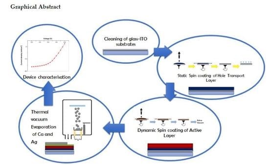
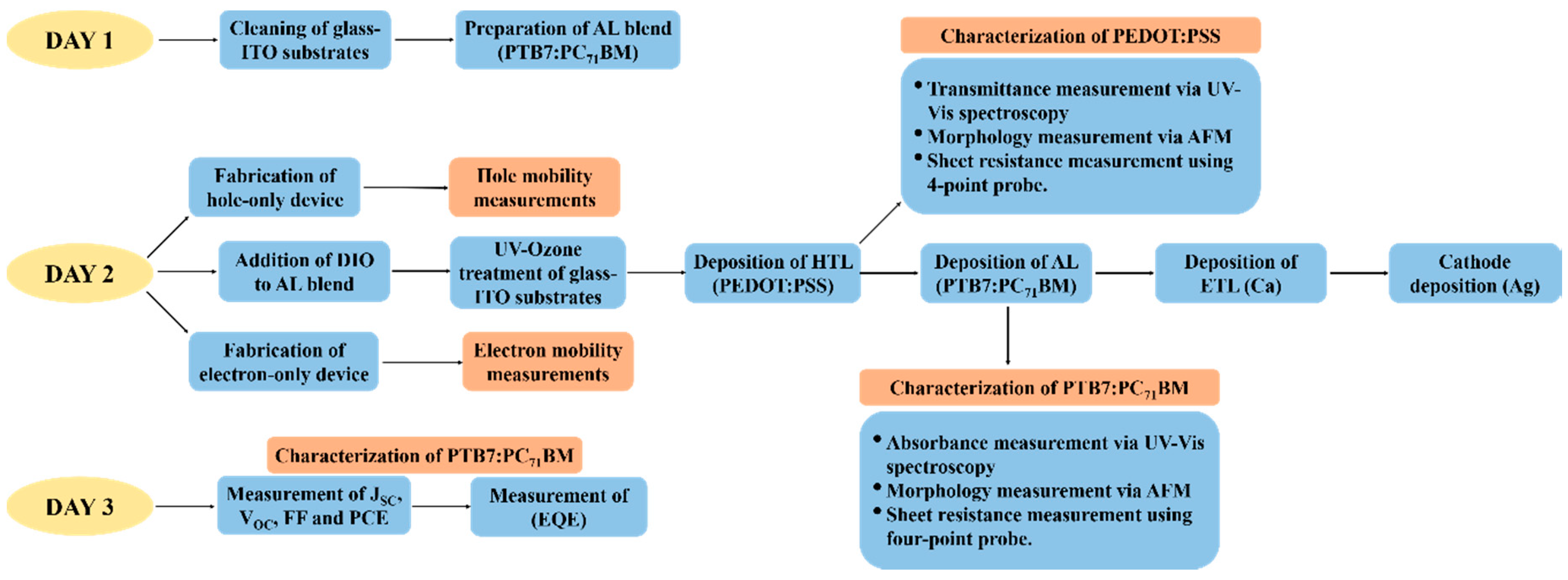
Figure 2.
The flow chart of the three days experiment step-by-step. ITO: indium-tin oxide; AL: active layer; ETL: electron transport layer; HTL: hole transport layer; EQE: external quantum efficiency; JSC: short circuit current density; VOC: open circuit voltage; FF: fill factor; PCE: power conversion efficiency; DIO: 1,8-Diiodooctane; AFM: atomic force microscopy.

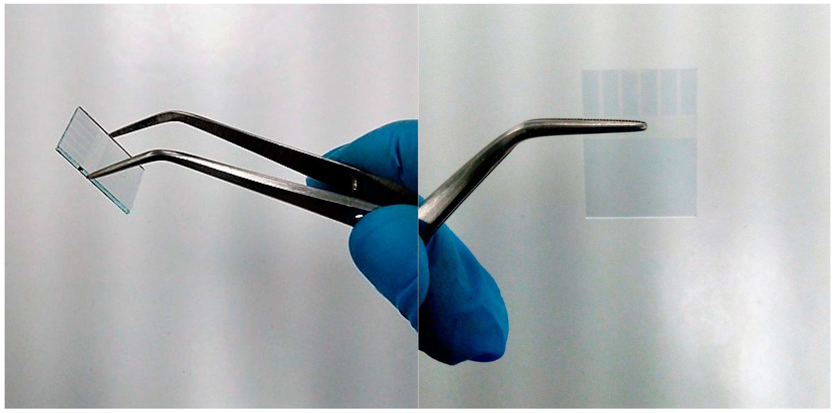
Figure 3.
The correct handling of the glass substrates with tweezers.

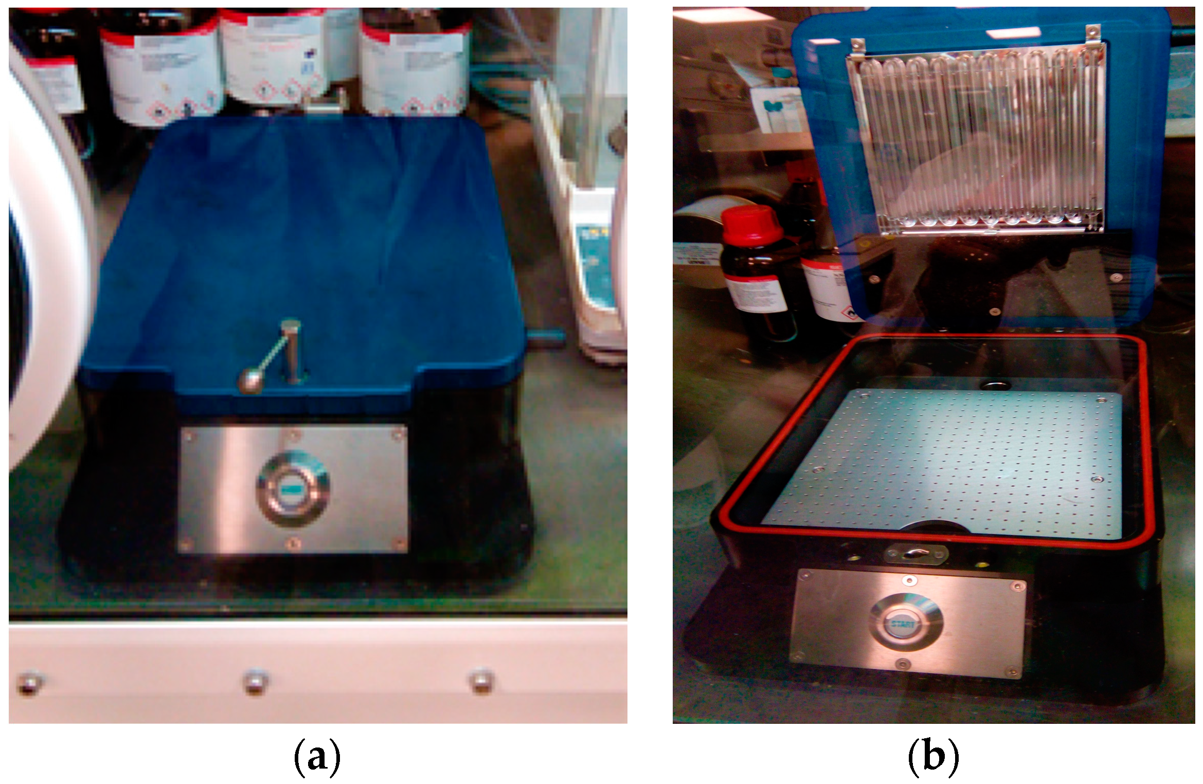
Figure 4.
UV-O3 cleaner used in the final step of the cleaning process of ITO-glass substrates shown both in the closed (a) and open position (b) and located inside the glove box.
Figure 4.
UV-O3 cleaner used in the final step of the cleaning process of ITO-glass substrates shown both in the closed (a) and open position (b) and located inside the glove box.

Figure 5.
Diagram depicting the HOMO and LUMO energy levels of a donor and an acceptor pair. Also shown, the work function (WF) values of the ITO anode, the PEDOT:PSS HTL, the calcium electron transport layer (ETL), and the silver cathode.
Figure 5.
Diagram depicting the HOMO and LUMO energy levels of a donor and an acceptor pair. Also shown, the work function (WF) values of the ITO anode, the PEDOT:PSS HTL, the calcium electron transport layer (ETL), and the silver cathode.

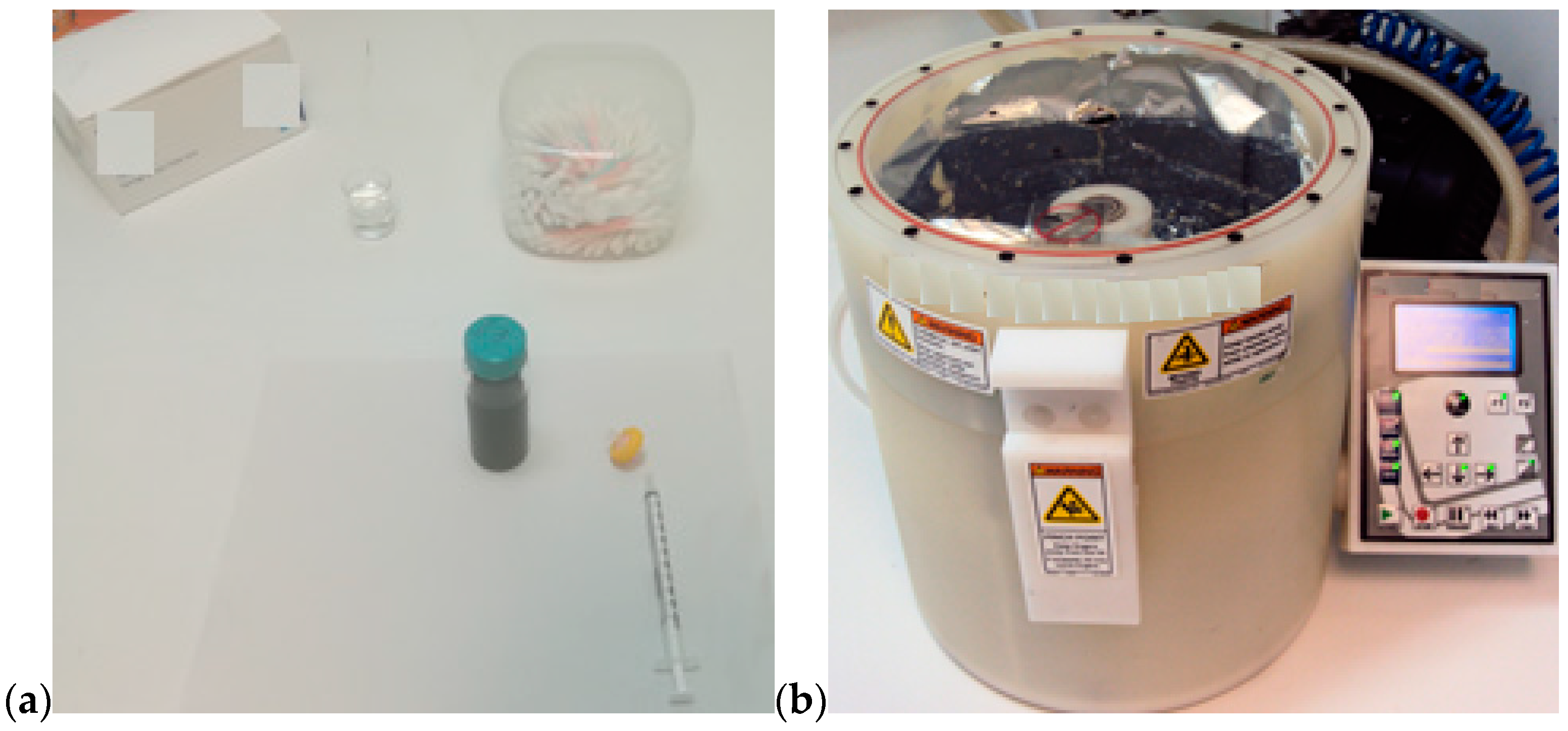
Figure 6.
(a) Materials and equipment for deposition of PEDOT:PSS; the hole transport layer (HTL), (b) spin coater used for the static spin coating of PEDOT:PSS.
Figure 6.
(a) Materials and equipment for deposition of PEDOT:PSS; the hole transport layer (HTL), (b) spin coater used for the static spin coating of PEDOT:PSS.

Figure 7.
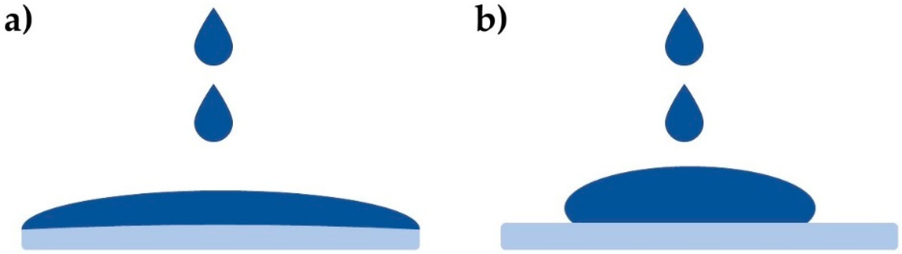
Schematic depicting the way PEDOT:PSS spreads onto (a) a UV-O3 treated glass-ITO substrate and (b) a non-UV-O3 treated glass ITO substrate. The UV-O3 treatment increases the hydrophilicity if the ITO surface thus ensuring that the aqueous PEDOT:PSS solution spreads more evenly on the entire area.
Figure 7.
Schematic depicting the way PEDOT:PSS spreads onto (a) a UV-O3 treated glass-ITO substrate and (b) a non-UV-O3 treated glass ITO substrate. The UV-O3 treatment increases the hydrophilicity if the ITO surface thus ensuring that the aqueous PEDOT:PSS solution spreads more evenly on the entire area.

Figure 8.
Transmittance spectrum for PEDOT:PSS film with a thickness of 25 nm deposited on ITO anode.
Figure 8.
Transmittance spectrum for PEDOT:PSS film with a thickness of 25 nm deposited on ITO anode.

Figure 9.
Surface image taken from atomic force microscopy (AFM) measurement for a PEDOT:PSS film spin coated onto a glass-ITO substrate. Reproduced with the permission from Krassas et al. [27], RSC Advances; published by The Royal Society of Chemistry, 2015.
Figure 9.
Surface image taken from atomic force microscopy (AFM) measurement for a PEDOT:PSS film spin coated onto a glass-ITO substrate. Reproduced with the permission from Krassas et al. [27], RSC Advances; published by The Royal Society of Chemistry, 2015.

Figure 10.
UV-Vis absorption spectrum for PTB7:PC71BM BHJ film with a thickness of 85 nm deposited onto the previous PEDOT:PSS film.
Figure 10.
UV-Vis absorption spectrum for PTB7:PC71BM BHJ film with a thickness of 85 nm deposited onto the previous PEDOT:PSS film.

Figure 11.
Surface image taken from AFM measurement for PTB7:PC71BM which is deposited directly onto PEDOT:PSS layer via dynamic spin coating. Reproduced with the permission from Stylianakis et al. [17], Dyes and Pigments; published by Elsevier, 2017.
Figure 11.
Surface image taken from AFM measurement for PTB7:PC71BM which is deposited directly onto PEDOT:PSS layer via dynamic spin coating. Reproduced with the permission from Stylianakis et al. [17], Dyes and Pigments; published by Elsevier, 2017.

Figure 12.
(a) Hole current density-(V-Vbi)2 graph obtained for a bulk heterojunction organic solar cell based on PTB7:PC71BM. (b) Electron current density-(V-Vbi)2 graph obtained for a bulk heterojunction organic solar cell based on PTB7:PC71BM. The hole mobility and electron mobility values are calculated by adding the respective JSC values to the Mott–Gurney equation (Equation (3)) and solving for μ.

Figure 13.
(a) J–V curve for organic photovoltaic device based on PTB7-PC71BM. (b) The fill factor demonstrated graphically on the J–V curve. Image remains the copyright of Ossila Ltd. Taken with permission from Ossila Ltd. [29].
Figure 13.
(a) J–V curve for organic photovoltaic device based on PTB7-PC71BM. (b) The fill factor demonstrated graphically on the J–V curve. Image remains the copyright of Ossila Ltd. Taken with permission from Ossila Ltd. [29].

Figure 14.
The test board used for making electrical connections to the photovoltaic devices. The substrate is placed in the center of the board and the cell which is to be characterized is selected using the respective switches. Image remains the copyright of Ossila Ltd. Taken with permission from Ossila Ltd. [29].

Figure 15.
Mask purchased from Ossila used to create the cathode pattern during the deposition of Ag via vacuum thermal evaporation (VTE). Image remains the copyright of Ossila Ltd. Taken with permission from Ossila Ltd. [29].
Figure 15.
Mask purchased from Ossila used to create the cathode pattern during the deposition of Ag via vacuum thermal evaporation (VTE). Image remains the copyright of Ossila Ltd. Taken with permission from Ossila Ltd. [29].

Figure 16.
(a) Complete fabricated bulk heterojunction organic solar cells (BHJ OSC). The silver area is the Ag cathode. The pattern is created with the mask utilized during Ag deposition via vacuum thermal evaporation (VTE). (b) The blue squares superimposed onto the photograph indicate the active area of the device.

Figure 17.
EQE curve obtained for PTB7:PC71BM active layer blend.


Table 1.
Chemical structures/formulas of the compounds used in the fabrication of the organic solar cell devices.
Table 1.
Chemical structures/formulas of the compounds used in the fabrication of the organic solar cell devices.
| Structure | Name | Role in the Organic Solar Cell |
|---|---|---|
| In2O3/SnO2 | ITO | Anode electrode |
 | PEDOT:PSS | Hole transport/electron blocking layer |
 | PTB7 | Electron donor in the photoactive layer blend |
 | PC71BM | Electron acceptor in the photoactive layer blend |
| Ca | Calcium | Electron transport/hole blocking layer |
| Al | Aluminum | Cathode electrode |
 | MoO3 | Hole transport layer/hole mobility measurements |
 | PFN | Electron transport layer/electron mobility measurements |
Table 2.
Conjugated polymers typically used as electron donors with PC71BM as the electron acceptor in organic solar cells. Included are the energy levels of the HOMO and LUMO levels, the ΔELUMO and the Eg value of each donor polymer.
Table 2.
Conjugated polymers typically used as electron donors with PC71BM as the electron acceptor in organic solar cells. Included are the energy levels of the HOMO and LUMO levels, the ΔELUMO and the Eg value of each donor polymer.
| PC71BM | Donor Polymer | LUMO of Donor Polymer | HOMO of Donor Polymer | ΔELUMO | Egdonor |
| P3HT | −3 eV | −5.20 eV | 0.9 eV | 2 eV | |
| PCDTBT | −3.6 eV | −5.45 eV | 0.3 eV | 1.8 eV | |
| PTB7-Th | −3.66 eV | −5.24 eV | 0.24 eV | 1.58 eV | |
| PTB7 | −3.31 eV | −5.12 eV | 0.59 eV | 1.81 eV |
Table 3.
Common organic materials typically used as electron acceptors with PTB7 as the electron donor in organic solar cells. Included are the energy levels of the HOMO and LUMO levels, the ΔELUMO and the Eg value of each acceptor material.
Table 3.
Common organic materials typically used as electron acceptors with PTB7 as the electron donor in organic solar cells. Included are the energy levels of the HOMO and LUMO levels, the ΔELUMO and the Eg value of each acceptor material.
| PBT7 | Acceptor Material | LUMO of Acceptor Material | HOMO of Acceptor Material | ΔELUMO | Egacceptor |
| ICBA | −3.8 eV | −5.80 eV | 0.5 eV | 2 eV | |
| PDIs | −3.70–−4 eV | −5.70–−6 eV | 0.4–0.7 eV | 1.70–2.30 eV | |
| SubPcs | −3.50 eV | −5.70 eV | 0.4 eV | 2.20 eV |
Table 4.
Photovoltaic parameters of a state-of-the-art bulk heterojunction organic solar cell fabricated PTB7:PC71BM as the active layer blend.
Table 4.
Photovoltaic parameters of a state-of-the-art bulk heterojunction organic solar cell fabricated PTB7:PC71BM as the active layer blend.
| JSC (mA/cm2) | VOC (V) | FF (%) | PCE (%) | |
|---|---|---|---|---|
| Optimum Device | 16.32 | 0.76 | 59.6 | 7.32 |
© 2019 by the authors. Licensee MDPI, Basel, Switzerland. This article is an open access article distributed under the terms and conditions of the Creative Commons Attribution (CC BY) license (http://creativecommons.org/licenses/by/4.0/).
Share and Cite
MDPI and ACS Style
Anagnostou, K.; Stylianakis, M.M.; Petridis, K.; Kymakis, E. Building an Organic Solar Cell: Fundamental Procedures for Device Fabrication. Energies 2019, 12, 2188. https://doi.org/10.3390/en12112188
AMA Style
Anagnostou K, Stylianakis MM, Petridis K, Kymakis E. Building an Organic Solar Cell: Fundamental Procedures for Device Fabrication. Energies. 2019; 12(11):2188. https://doi.org/10.3390/en12112188
Chicago/Turabian StyleAnagnostou, Katerina, Minas M. Stylianakis, Konstantinos Petridis, and Emmanuel Kymakis. 2019. "Building an Organic Solar Cell: Fundamental Procedures for Device Fabrication" Energies 12, no. 11: 2188. https://doi.org/10.3390/en12112188
Note that from the first issue of 2016, this journal uses article numbers instead of page numbers. See further details here.