
A New Backward Euler Stabilized Optimum Controller for NPC Back-to-Back Five Level Converters
by
 , ,
, ,
Miguel Chaves
1,3,4,*, 
José Fernando Silva
2,3,
Sónia Ferreira Pinto
2,3,
Elmano Margato
1,3,4 and
João Santana
2,3 1
Instituto Superior de Engenharia de Lisboa (ISEL), Instituto Politécnico de Lisboa, Rua Conselheiro Emídio Navarro 1, Lisboa 1959-007, Portugal
2
Departamento de Engenharia Eletrotécnica e de Computadores, Instituto Superior Técnico, TU Lisbon, Av. Rovisco Pais 1, Lisboa 1049-001, Portugal
3
Instituto de Engenharia de Sistemas e Computadores, Investigação e Desenvolvimento em Lisboa (INESC-ID), R. Alves Redol 9, Lisboa 1000-029, Portugal
4
Centro de Eletrotecnia e Eletrónica Industrial (CEEI), Rua Conselheiro Emídio Navarro 1, Lisboa 1959-007, Portugal
*
Author to whom correspondence should be addressed.
Energies 2017, 10(6), 735; https://doi.org/10.3390/en10060735
Submission received: 20 March 2017
/
Revised: 5 May 2017
/
Accepted: 9 May 2017
/
Published: 23 May 2017
(This article belongs to the Special Issue Power Electronics in Power Quality)
Abstract
:This paper presents a backward Euler stabilized-based control strategy applied to a neutral point clamped (NPC) back-to-back connected five level converters. A generalized method is used to obtain the back-to-back NPC converter system model. The backward Euler stabilized-based control strategy uses one set of calculations to compute the optimum voltage vector needed to reach the references and to balance the voltage of the DC-bus capacitors. The output voltage vector is selected using a modified cost functional that includes variable tracking errors in the functional weights, whereas in classic approaches, the weights are considered constant. The proposed modified cost functional enables AC current tracking and DC-bus voltage balancing in a wide range of operating conditions. The paper main contributions are: (i) a backward Euler stabilized-based control strategy applied to a double, back-to-back connected, five level NPC converter; (ii) the use of cost functional weight varying as a function of the controlled variable tracking errors to enforce the controlled variables and to balance the DC capacitor voltages; and (iii) the demonstration of system feasibility for this type of converter topology and control strategy, ensuring a high enough computational efficiency and extending the modulation index from 0.6 to 0.93. Experimental results are presented using a prototype of a five level NPC back-to-back converter.
1. Introduction
Multilevel power converters are the converters of choice for high power medium voltage applications such as electrical machine drives or the grid interface connection of renewable energy sources [1,2,3,4]. Considering today’s power semiconductor limitations on voltage blocking and dv/dt, the attention and development of multilevel voltage source converters is increasing due to known attractive features, when compared with two level voltage source converters [5,6,7,8].
Among multilevel converters, the neutral point clamped (NPC) converter introduced in [5] is well accepted and used in several industrial applications [7]. The main drawback of the NPC topology is the voltage imbalance of the DC-bus capacitors, which has been an active research topic using external circuits [8,9], modifying pulse width modulation (PWM) techniques [10,11,12,13], space vector modulation (SVM) [3,4,14], sliding mode control exploiting converter vector redundancies [15], and predictive control [16,17,18]. Some of these techniques require a significant computing power, or have limitations when redundant vector-based strategies are used to balance the capacitor voltages. The theoretical maximum output modulation index is around 0.6 for a back-to-back connected NPC converter with an active load and zero active power exchange, when using the SVM-based control strategy [3,4].
Known NPC modulation strategies such as PWM and SVM [10,12] while operating at a constant switching frequency, do not guarantee that controlled outputs are free from DC-bus voltage disturbances, semiconductor “ON” voltages, dead times, or switching delays.
Hysteretic control methods are robust to semiconductor non-idealities, load changes, and disturbances, and present fast dynamic responses. Their major drawback is the variable switching frequency, which depends on the operating conditions and load parameters. For some quality indexes, hysteretic control methods may need higher switching frequencies when compared to PWM or SVM modulation techniques [17,18].
Optimum predictive control techniques drive the output errors towards zero by minimizing the cost functional in each sampling period [19,20,21,22]. Given the controlled output references, the first step of the NPC predictive controller is to sample the state variables. The second step uses a non-linear model of the system to predict values of the state variables in the next sampling intervals for every possible NPC switching configuration (termed the vector). This requires a powerful numerical processor to compute all the possible future values of the state variables in a sampling step well below 100 µs, to allow switching frequencies around 5 kHz. The last step computes the cost functional for all NPC vectors and chooses the vector that gives the minimum cost functional value in that sampling interval. These three steps are repeated in the next sampling time.
Predictive controllers for power electronic converters seem to be a potential alternative since they are well suited to control variables (e.g., currents, voltages, power) presenting coupled dynamics, and can offer closed loop dynamics with decoupled behavior [19]. However, in each sampling time, predictive algorithms must compute the state variable values in the next sampling interval for all of the possible NPC vectors, together with the corresponding cost functional, requiring a powerful processing unity for converters with available vectors in excess of 27 (three level converters).
Predictive algorithms used to reduce time consumption have been reported by [23,24]. These algorithms use the system inverse dynamics to directly compute the necessary output voltage vector required to track references, while predictive controllers estimate the output errors for all the available vectors. The output voltage vector is then selected among those which are available by minimizing a cost functional that computes the distance between the optimal voltage vector and the existing voltage vectors. However, in [23], the voltage balancing problem was not addressed but only pointed out briefly in cases where the converter presented redundancies. In [24], the voltage balancing problem was solved for three level inverters, but the dependence on non-modeled dynamics is not addressed. This paper uses a stable method to compute the necessary output voltage vector and extends the voltage balancing to five level NPC converters, where balancing is more challenging, by using an approach that is valid even if there are no redundant vectors. In [24], only constant weights are used in the quadratic cost function, while the proposed paper uses variable weights as a function of variable tracking errors, for the cost functional equations of functions. The approach proposed here, while not needed in three level NPCs, is nearly mandatory in five level inverters, as balancing the four DC capacitor voltages using 250 vectors is, at least, more complex and difficult. The approach of this paper enables the enlargement of NPC voltage balancing range for different active and reactive power flow conditions. In view of these problems, this paper presents a backward Euler stabilized control strategy applied to a back-to-back five level NPC converter to control the line inject AC currents and to balance the four capacitor voltages. The paper starts with the back-to-back converter modeling, using a systematic switching variable generalized for m level converters (Section 2). This modeling is an essential tool for the analysis and control strategy of the NPC back-to-back converter. The control strategy proposed (Section 3) uses a backward Euler stabilized approach to directly compute the optimum output voltage vector required to track the references in the next time step. The output voltage vector is then selected from the available voltage vectors by minimizing a variable weight cost functional that includes variable tracking errors in the weighting of the error between the optimal voltage vector and the possible voltage vectors. The new proposed cost function enables active and reactive power flow control and DC-bus voltage balancing, in a wide range of operating conditions. Simulation and experimental results for two five level NPC back-to-back connected converters validate the proposed control strategy and show the feasibility of the proposed system (Section 4). Experimental results are obtained using a 230 V ac/600 V dc/230 V ac five level NPC back-to-back converter prototype. Both converters are controlled using one Power PC-based board (DS1103) with a 32 µs sampling time, for acquiring all the data, completing the calculations of the two 125 vectors converters, and computing the gate signals to drive all the 48 IGBTs.
2. System Modeling
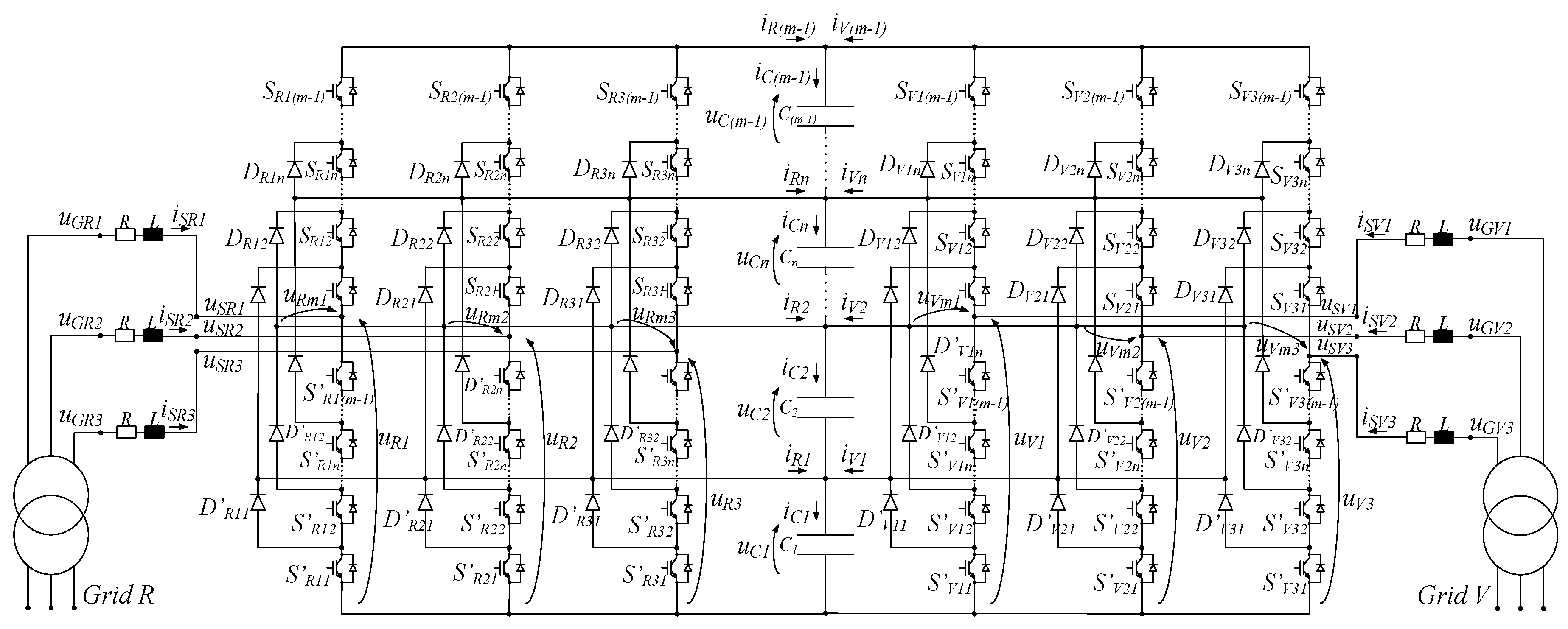
Figure 1 shows the m level back-to-back converter arrangement. The generalized system is composed by two three phase back-to-back m level diode-clamped converters, where each NPC converter is connected to an AC system using a transformer. The modeling assumes ideal electrical components and semiconductor devices (zero ON voltages, zero OFF currents, zero switching times).
To obtain a model valid for NPC multilevel converters having an arbitrary number of levels m, it is advantageous to start numbering the upper IGBT switches Sk1, Sk2, … Skn, … Sk(m−1) in each k leg (k ∈ {1, 2, 3}) from the leg midpoint, and S’k1, S’k2, … S’kn, … S’k(m−1) up from the zero voltage node. The DC-bus capacitors are also numbered up from the zero voltage point. Each semiconductor and DC-bus capacitor index is associated with the respective voltage level.
The switching strategy for an m level NPC converter ensures that the upper leg switches [Sk1 Sk2 … Skn … Sk(m−1)] and the corresponding ones on the lower side [S’k1 S’k2 … S’kn … S’k(m−1)] are always in complementary states. Consequently, if Skn = 1, then S’kn must be equal to 0, where Skn = 1 means that the specified switch is ON, and Skn = 0 shows that the switch is OFF.
2.1. Converter Generalized State Space Model
For each NPC leg, the output voltage variables uk (uRk or uVk for the R-side converter and V-side converter, respectively) are defined from the k leg midpoint to zero voltage. The output voltage can be written in terms of the logical state of the leg switches Skn and DC-bus capacitor voltages, as in (1), where, is the voltage of the nth dc-link capacitor.
Considering a three phase balanced network, the k phase voltage uSk can be related to all leg output voltages uk and, using (1), expressed as a function of the DC-bus capacitor voltages as (2), where the elements SUkn are determined by (3).
The DC-bus n level current in can be related to the phase currents iSk by (4):
where γnk is a time dependent switching variable, written in terms of the k leg switching logical states (5), as follows:
At each time, the load phase current iSk is connected to an n DC-bus level when γnk = 1, or to the zero voltage bus when γnk = 0.
Each DC-bus n level current capacitor can be related to the corresponding voltage by (6):
The above current can be expressed in terms of the upper capacitor current and the corresponding DC-bus n level currents from the grid side iRn or iVn, by (7):
Using Equations (4), (6), and (7) for both grid sides, the voltage capacitor time derivative is expressed in terms of the phase currents, iSRk and iSVk, as it is shown in (8):
where the k column matrix element, or (k leg), is determined using the value of the time dependent switching variable, γRnk or γVnk, in the case of the R or V side, respectively, as (9) and (10):
Applying the Concordia transformation [25] to Equations (2) and (8) and considering that zero sequence components are null, the multilevel converter matrix equations in the αβ coordinates are given by (11) and (12), as follows:
where, Гνα, Гνβ, SUnα, and SUnβ are obtained by applying the αβ0 transformation to the Гn1, Гn2, Гn3, and SUn1, SUn2, SUn3 variables.
2.2. Grid Side Interface Modeling
The time derivative of the k phase current of the R-side or V-side converter in αβ coordinates, iSαβ, is obtained using (13), where uGαβ is the grid voltage, R and L represent the grid connection per phase of resistance and inductance, and uSRαβ is the converter AC output voltage.
3. Backward Euler Stabilized Optimum Control
3.1. Global System Control
The control structure of the NPC back-to-back converter system, shown in Figure 2, uses two controllers, one for each converter side. The R-side NPC controls the R-side AC currents, enforcing the DC-bus voltage udc (therefore ensuring energy balancing), and establishing the reactive power injected in the R-side grid. Additionally, it balances the capacitor voltages. The V-side NPC controls the V-side AC currents (establishing the active and reactive power to be delivered to the V-side), and balances the capacitor voltages. The power flow control enforces, via the udc bus voltage or directly, both R and V sides sinusoidal AC current references. Each NPC will be provided with one independent vector selection controller.
The R-side converter maintains the DC-bus voltage udc at a given reference using a Proportional-Integral (PI) controller. From the udc controller output, a reference value for the grid current d component iSRdref is obtained, enforcing the active power demanded from the R grid. The reactive power reference QRref is used to obtain the grid current q component reference iSRqref. These current reference values, as well as the grid currents iSR123 and the capacitor voltages uC1…uC4, are the inputs of the backward Euler Stabilized optimum controller, whose output is the three phase vector to be applied by the converter (a b c).
The V-side controller controls the active power PV and reactive power QV on the V-side grid. The reference value of the grid current d component iSVdref is established from the reference of the active power flow. The reference value of the grid current q component iSVqref is established from the reactive power reference. The reference currents iSVdqref, together with the grid currents iSV123 and capacitor voltages, are the inputs of the backward Euler Stabilized optimum controller vector selection block. This controller also balances the capacitor voltages around their reference values.
3.2. Backward Euler Stabilized Optimum Current Control and Capacitor Voltage Balancing
3.2.1. AC Current Control
Using the stable Euler backward approach [26], the current values in the next time step, can be obtained from (14):
This is an implicit method used to solve stiff differential equations. Under the Lipschitz continuity assumption on the current derivative, it can be shown that if Ts is small enough, the Equation (14) has a unique solution. In addition, the Euler backward method is absolutely stable [26]. The backward Euler method is therefore very useful because its stability region contains the whole left half of the complex plane.
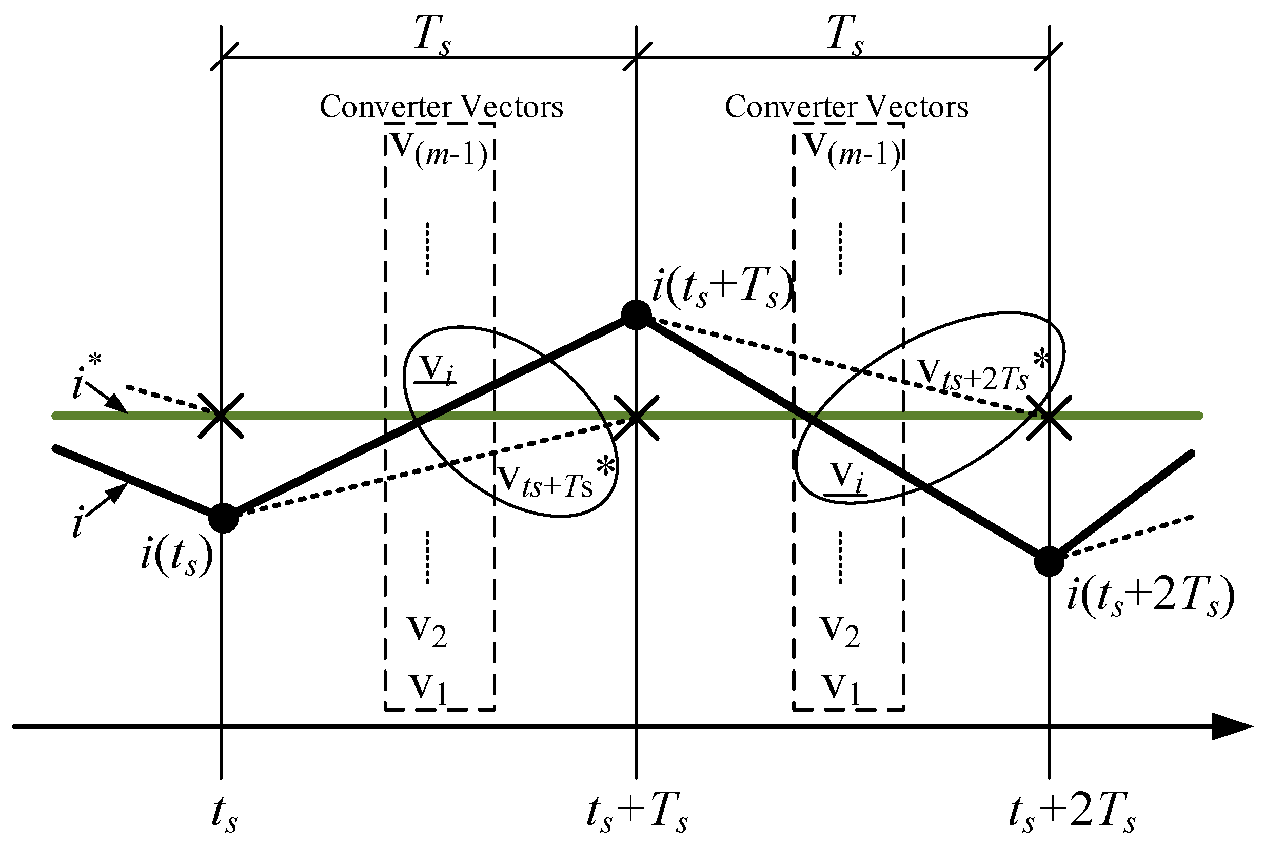
Using (14) and (13), the optimum vector that assures the references tracking in the next time step, and components, denoted , is computed as (15):
From (15), it is possible to compute the optimum converter voltage vector components VI = needed, so that the iSαβ current vector is equal to its reference at the next sampling time = . The optimum vector VI = [, ]T is only computed once in each sampling step and is used in the cost functional equations in order to select the best vector to be applied in the converter. Figure 3 shows a diagram of the backward Euler stabilized optimum control principle, where the selected vector is the one that minimizes a weighted distance to the optimum vector.
3.2.2. Voltage Balancing Control
Similar to current control and using the Euler backward approach, each capacitor optimal current that leads the nth capacitor voltage towards the reference uCref in the next sampling time, = , can be estimated using (16) as a discrete time approximation of (6). All the DC-bus capacitors have the same value for their voltage reference uCref. For each level, the total DC-bus level currents, or , are obtained using (17).
Therefore, the needed DC-bus currents to be applied in the following time step in order to assure the desired capacitor voltages, can be written as a vector form IU in (18):
The NPC converter available capacitor current vectors can be computed using Equation (19). is computed for each converter voltage vector Vi (uSαi, uSβi), considering that the phase currents will approximately follow their references in the next sampling time. Equation (19) is applied separately to both converter sides.
3.2.3. Cost Functional and Vector Selection
The vector selection strategy, applied to both converters independently, minimizes a cost functional (20), relating the weighted distances to the optimum vectors, where WI(iSk), and are the weights of errors and between the references and the values obtained from the application of each NPC vector Vi, respectively.
In (20), the vector error is given by (21) and evaluates the distance between the current control optimal-vector VI (, ), and the ist NPC available vector Vi = [, ]. It gives the information of the optimal-vector VI deviation from the possible vector Vi.
Moreover, the error , given by (22), is the converter ist DC-bus current vector deviation from the optimal current vector IU, which is necessary to balance the capacitor voltages. From (18) and (19):
The phase current control is further associated with the weight WI(iSk) of the cost functional (20) given in (23), showing that it depends on the current tracking error. In (23), ρI is a constant for all possible vectors and is used to match current error units, which are weighted with voltage error units.
If only AC current control was required, a constant weight WI(iSk) in (20) would be enough. However, since it is also necessary to balance the capacitor voltages, it is better to consider a quadratic form (23) of WI(iSk) in the cost functional, in order to give greater weight to the current error when bigger tracking errors occur.
The DC capacitor voltage balance is not the main purpose of NPC converter control, but it is nevertheless an essential task to enable the NPC correct operation. Thus, in the cost functional (20), the weight imposes the need to balance the capacitor voltages. It is given by (24) as a quadratic function of the capacitors’ voltage tracking errors sum, where ρC is considered to be a constant value.
The variable weighting strategy, WI(iSk), and , give greater attention, either to the current control or to DC-bus voltages balancing control as a function of tracking errors, without needing to compute the controlled variable values for every possible converter vector. This flexibility allows covering a larger range of NPC operating conditions.
The cost functional (20) is calculated for each NPC possible vector Vi, including the redundant vectors. The selected vector is the one that scores the minimum value for the cost functional fC(Vi).
4. Simulation and Experimental Results
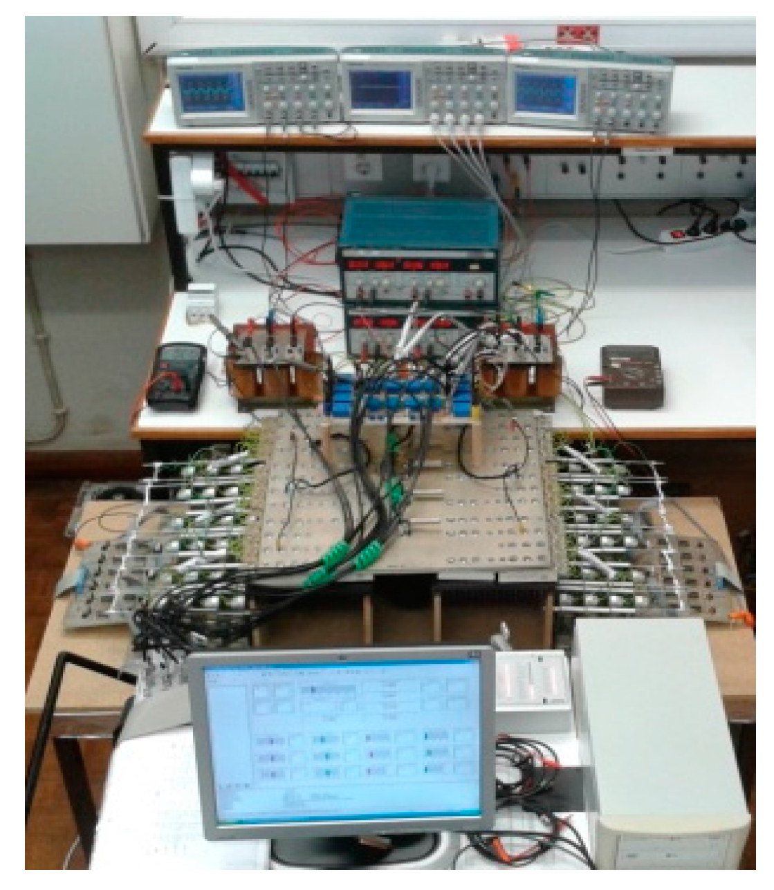
The proposed system simulations and experimental results, shown in the following points, were obtained using a 230 V ac/600 V dc/230 V ac five level NPC back-to-back prototype, shown in Figure 4. This prototype uses 48 IGBTs (Semikron Elektronik Gmbh & Co., Nuremberg, Germany) as controlled power semiconductors. Both five level NPC converters are controlled using just one Power PC-based board (DS1103 from dSPACE GmbH, Paderborn, Germany) with a 32 μs sampling time, which performs sampling and calculations, and outputs semiconductor signals. The system parameters are presented in Table 1.
4.1. Current Control
Table 2 presents the steady state operation conditions used in the experimental result shown in Figure 5. This figure shows the phase current iSV1 experimental result and the respective frequency spectrum. From Figure 5, it is possible to see that the output phase currents exhibit the fundamental component at 50 Hz and also a spread spectrum with a maximum frequency around 5 kHz. This maximum frequency is well above each semiconductor switching frequency, since the output switching frequency is the contribution of the eight IGBTs of each one of the three converter legs.
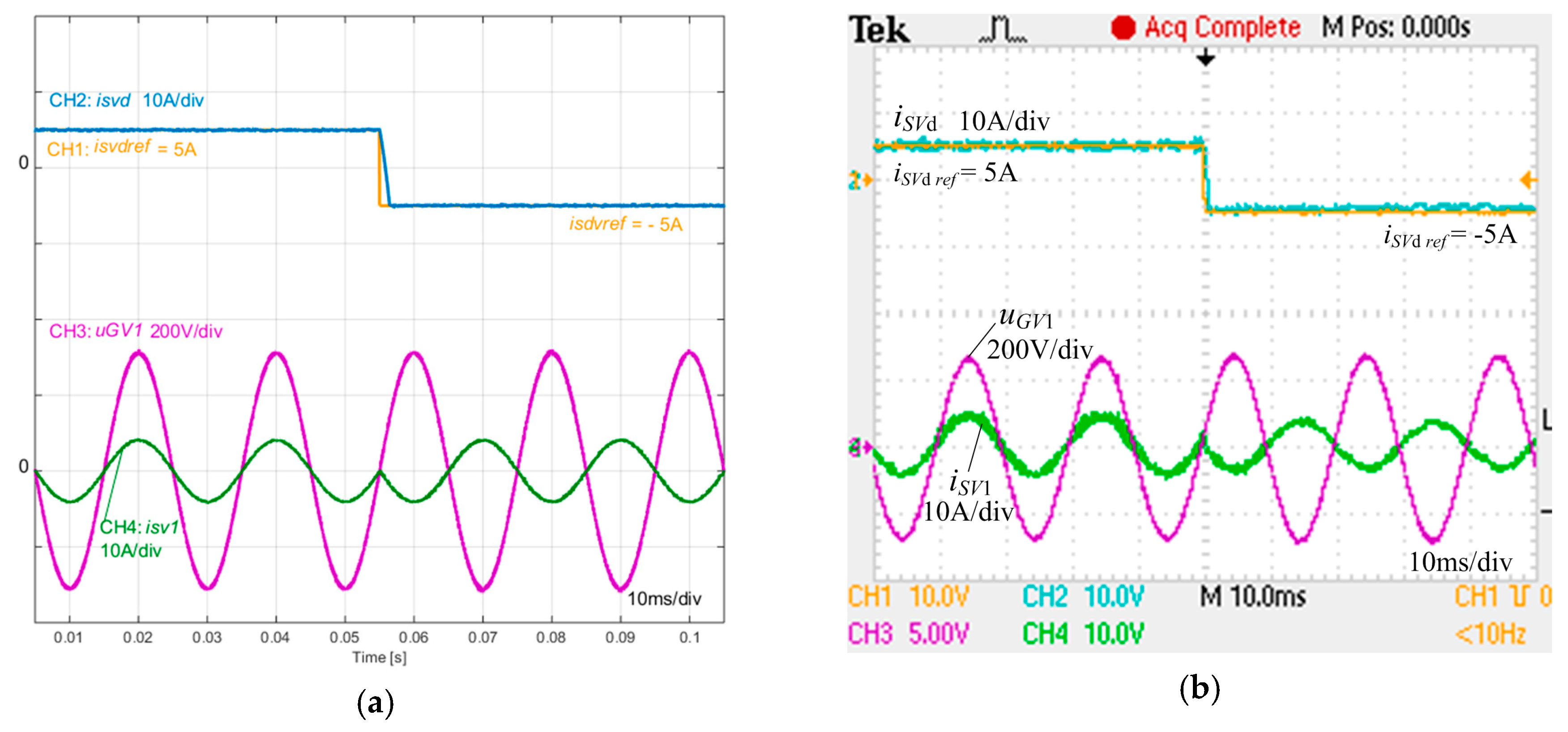
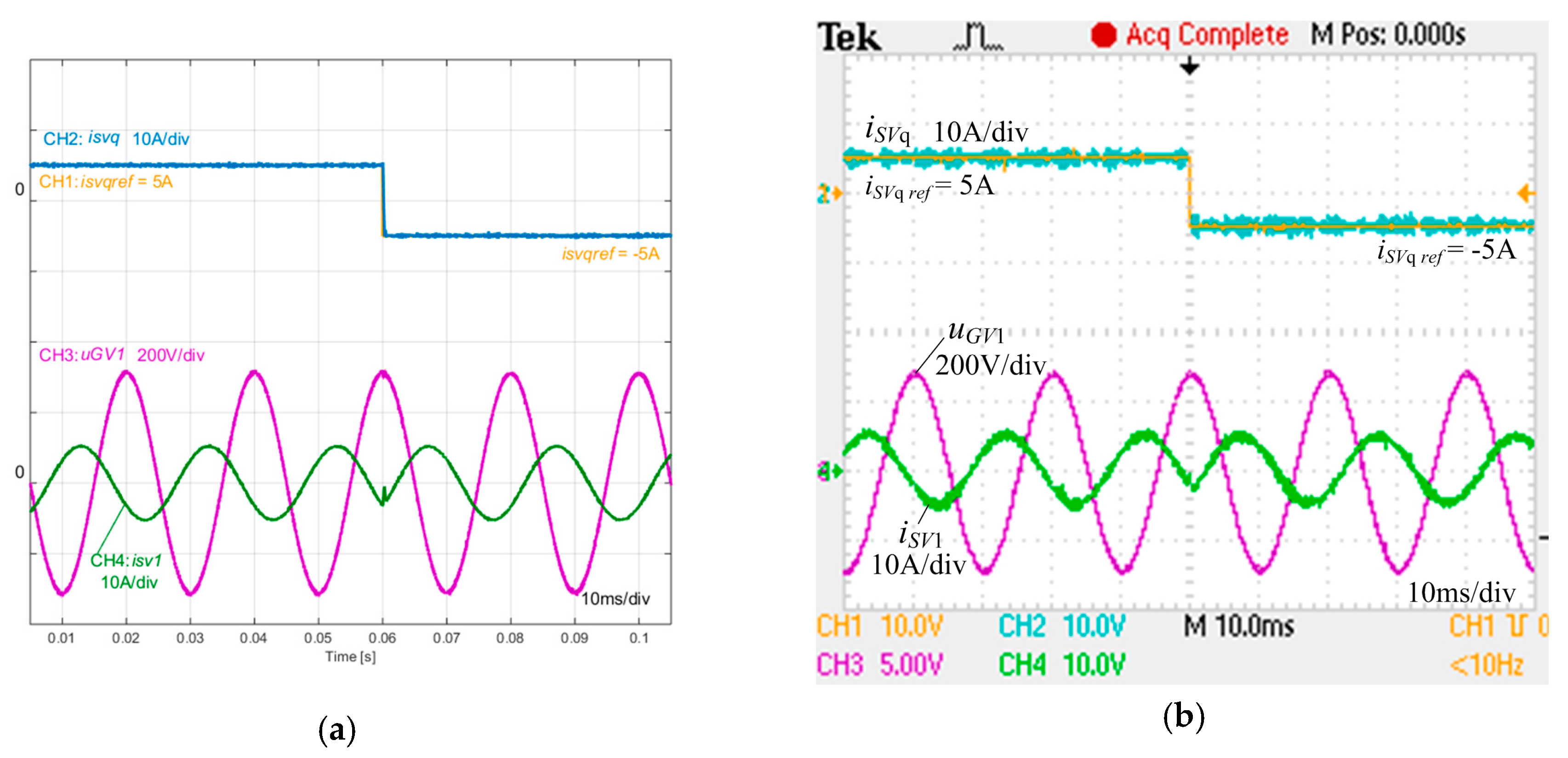
Table 3 presents the operation conditions used to obtain the simulation results of Figure 6a and Figure 7a, and the corresponding experimental results shown in Figure 6b and Figure 7b. These figures show the phase current iSV1 control during a step in the iSVd and iSVq reference, respectively.
From Figure 6 and Figure 7, it can be seen that the backward Euler stabilized control strategy accurately tracks the current references in a steady state or during a step in the iSVd or iSVq reference, respectively. The measured current ripple was less than 0.25 A in 5 A (<5%).
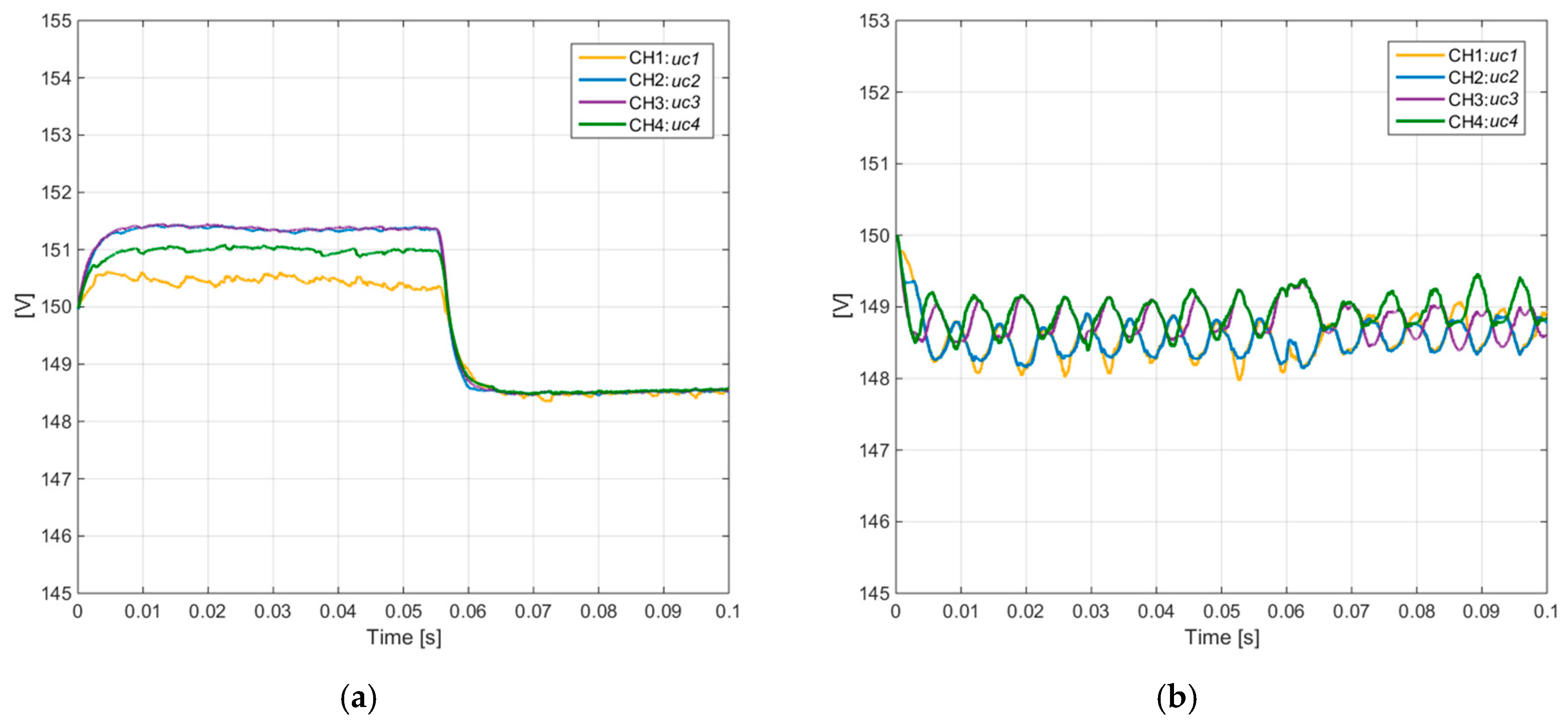
The time evolution of the capacitor voltages during the step transitions of Figure 6 and Figure 7 are presented in Figure 8a,b respectively. From Figure 8, it can be seen that the deviation of the capacitor voltages, uC1…4, is around 1.5 V over 150 V (1%).
The proposed control strategy achieves high output modulation indexes, , even in the most difficult operation conditions for a NPC back-to-back connection with an active load, that is, with no active power exchange [4]. Table 4 shows the operation conditions of the simulation results presented in Figure 9, and displays the 1st harmonic uGV12-1h of the output line-to-line voltage.
The simulation results of Figure 9 were obtained using a modulation index around mo = 0.93. This result clearly shows the limits extension of the proposed control strategy, when compared with redundant vector-based strategies as sinusoidal pulse width modulation (SPWM) or space vector modulation (SVM) [3,4] (the theoretical maximum output modulation index is around 0.6).
4.2. DC-bus Voltage Control and Capacitors Voltage Balancing
DC-bus voltage control robustness is verified by applying a grid side voltage sag perturbation of a 25% nominal voltage, for which the operation conditions are presented in Table 5 and the results are shown in Figure 10. It can be seen that the DC-bus voltage remains almost constant through a sag perturbation on the main grid voltage. The maximum voltage disturbance measured was 50 V in 600 V (<9%).
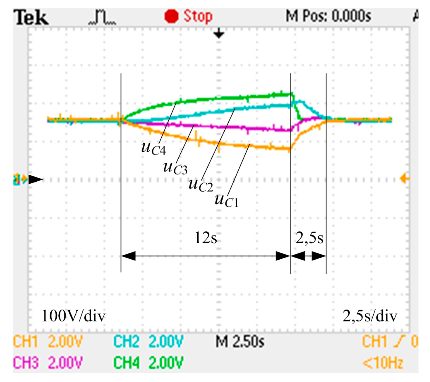
The voltage balancing of the capacitors is tested by restarting the voltage balancing algorithm, which means that ρC ≠ 0, after a time interval without considering it (ρC = 0). The operating conditions are presented in Table 6 and the results are shown in Figure 11. From Figure 11, it can be seen that the four capacitor voltages uC1…4 deviate from the reference during the time interval without voltage balancing. After restarting the voltage balancing algorithm, the backward Euler stabilized control strategy has the capability to rapidly restore the capacitor voltage balance.
4.3. Power Flow Control
Several conditions can be imposed in order to test power flow control. Figure 12 and Figure 13 show the iSVd reference, phase current, and udc voltage for two different power flow conditions, presented in Table 7.
From Figure 12 and Figure 13, it is possible to see the udc recovery after a negative or positive step in active power flow, respectively. The experimental results obtained attest the good performance of the proposed control strategy.
From [19,21,24], the comparison presented in Table 8 can be obtained. Although the results are not directly comparable, since some of them refer to three-level converters, while the herein results are for five-level converters, it can be said that the backward Euler-based controller shows results which are better than PI controllers and are comparable to the best results obtained by advanced controllers.
5. Conclusions
The proposed backward Euler stabilized control strategy based on a generalized model of a five level NPC back-to-back converter, is able to control both the converter AC currents and to balance the four capacitor voltages.
From the active and reactive power flow of the convertors, in addition to the DC-bus voltage references, the control strategy computes, using the stable backward Euler approach, the optimum voltage or current vectors required to reach the references in the next time step. The selection of the converter output voltage vector is done by minimizing a variable weight cost functional within a sampling period. The minimum value of the cost functional gives the converter output voltage vector. The modified cost functional with variable weight allows converter control in a wide range of operating conditions.
Simulation and experimental results were obtained using a 230 V ac/600 V dc/230 V ac five level NPC back-to-back prototype. Both NPC converters are controlled with one Power PC-based board (DS1103) with a 32 µs sampling time.
The results demonstrate the feasibility and robustness of the proposed control strategy, achieving a very good compromise covering the main tasks: AC current tracking errors were lower than 5% and the DC-bus capacitor voltage balancing was within 10%. When compared with redundant vector-based control techniques, the proposed control strategy shows the extension of the modulation index, from 0.6 to 0.93.
Acknowledgments
This work was supported in part by national funds through “Fundação para a Ciência e a Tecnologia” (FCT) with reference UID/CEC/50021/2013.
Author Contributions
M. Chaves, J. F. Silva and E. Margato conceived the theory and designed the experiments; M. Chaves performed the experiments; M. Chaves, S. F. Pinto and J. Santana analyzed the data; M. Chaves, J. F. Silva, S. F. Pinto J. and J. Santana wrote the paper.
Conflicts of Interest
The authors declare no conflict of interest.
References
- Franquelo, L.G.; Rodríguez, J.; Leon, J.I.; Kouro, S.; Portillo, R.; Prats, M.A.M. The age of multilevel converters arrives. IEEE Ind. Electron. Mag. 2008, 2, 28–39. [Google Scholar] [CrossRef]
- Natchpong, H.; Kondo, Y.; Akagi, H. Five-level diode-clamped PWM converters connected back-to-back for motor drives. IEEE Trans. Ind. Appl. 2008, 44, 1268–1276. [Google Scholar]
- Saeedifard, M.; Iravani, R.; Pou, J. A space vector modulation strategy for a back-to-back five-level HVDC converter system. IEEE Trans. Ind. Electron. 2009, 56, 452–466. [Google Scholar] [CrossRef]
- Pou, J.; Pindado, R.; Boroyevich, D.; Rodríguez, P. Limits of the neutral-point balance in back-to-back-connected three-level converters. IEEE Trans. Power Electron. 2004, 19, 722–731. [Google Scholar] [CrossRef]
- Nabae, A.; Takahashi, I.; Akagi, H. A new-neutral-point-clamped PWM inverter. IEEE Trans. Ind. Appl. 1981, 17, 518–523. [Google Scholar] [CrossRef]
- Rodríguez, J.; Lai, J.S.; Peng, F.Z. Multilevel inverters: A survey of topologies, controls, and applications. IEEE Trans. Ind. Electron. 2002, 49, 724–738. [Google Scholar] [CrossRef]
- Rodríguez, J.; Bernet, S.; Steimer, P.; Lizama, I. A survey on neutral-point-clamped inverters. IEEE Trans. Ind. Electron. 2010, 57, 2219–2230. [Google Scholar] [CrossRef]
- Khomfi, S.; Tolbert, M. Multilevel power converters. In Power Electronics Handbook, 2nd ed.; Rashid, M.H., Ed.; Elsevier: Amsterdam, The Netherlands, 2007; pp. 451–482. [Google Scholar]
- Shu, Z.; He, X.; Wang, Z.; Qiu, D.; Jing, Y. Voltage balancing approaches for diode-clamped multilevel converters using auxiliary capacitor-based circuits. IEEE Trans. Power Electron. 2013, 28, 2111–2124. [Google Scholar] [CrossRef]
- Holmes, D.G.; Lipo, T.A. Pulse Width Modulation for Power Converters; Wiley: Hoboken, NJ, USA, 2003. [Google Scholar]
- Busquets-Monge, S.; Ortega, J.D.; Bordonau, J.; Beristain, J.A.; Rocabert, J. Closed-loop control of a three-phase neutral-point-clamped inverter using an optimized virtual-vector-based pulse width modulation. IEEE Trans. Ind. Electron. 2008, 55, 2061–2071. [Google Scholar] [CrossRef]
- Kazmierkowski, M.P.; Malesani, L. Current control techniques for three-phase voltage-source PWM converters: A survey. IEEE Trans. Ind. Electron. 1998, 45, 691–703. [Google Scholar] [CrossRef]
- Grzesiak, L.M.; Tomasik, J.G. Novel DC link balancing scheme in generic n-level back-to-back converter system. In Proceedings of the 7th International Conference on Power Electronics, Daegu, Korea, 22–26 October 2007; pp. 1046–1049. [Google Scholar]
- Marchesoni, M.; Tenca, P. Diode-clamped multilevel converters: A practicable way to balance DC-link voltages. IEEE Trans. Ind. Electron. 2002, 49, 752–765. [Google Scholar] [CrossRef]
- Chaves, M.; Margato, E.; Silva, J.F.; Pinto, S.F. A new approach in back-to-back m level diode-clamped multilevel converter modeling and DC-bus voltages balancing. IET Power Electron. J. 2010, 3, 578–589. [Google Scholar] [CrossRef]
- Vargas, R.; Cortes, P.; Ammann, U.; Rodriguez, J.; Pontt, J. Predictive control of a three-phase neutral-point-clamped inverter. IEEE Trans. Ind. Electron. 2007, 54, 2697–2705. [Google Scholar] [CrossRef]
- Silva, J.F.; Pinto, S.F. Advanced Control of Switching Power Converters, Power Electronics Handbook 3/e; Rashid, M.H., Ed.; Elsevier: Amsterdam, The Netherlands, 2011; pp. 1037–1114. [Google Scholar]
- Verveckken, J.; Silva, J.F.; Barros, J.D.; Driesen, J. Direct power control of series converter of Unified power-flow controller with three-level neutral point clamped converter. IEEE Trans. Power Deliv. 2012, 27, 1772–1782. [Google Scholar] [CrossRef]
- Dionísio Barros, J.; Fernando Silva, J. Optimal predictive control of three-phase NPC multilevel converter for power quality applications. IEEE Trans. Ind. Electron. 2008, 55, 3670–3681. [Google Scholar] [CrossRef]
- Kouro, S.; Cortes, P.; Vargas, R.; Ammann, U.; Rodriguez, J. Model predictive control—A simple and powerful method to control power converters. IEEE Trans. Ind. Electron. 2009, 56, 1826–1838. [Google Scholar] [CrossRef]
- Dionísio Barros, J.; Fernando Silva, J. Multilevel optimal predictive dynamic voltage restorer. IEEE Trans. Ind. Electron. 2010, 57, 2747–2760. [Google Scholar] [CrossRef]
- Rodriguez, J.; Kazmierkowski, M.; Espinoza, J.; Zanchetta, P.; Abu-Rub, H.; Young, H.; Rojas, C. State of the art of finite control set model predictive control in power electronics. IEEE Trans. Ind. Inform. 2013, 9, 1003–1016. [Google Scholar] [CrossRef]
- Pérez, M.A.; Cortés, P.; Rodríguez, J. Predictive control algorithm technique for multilevel asymmetric cascaded H-bridge inverters. IEEE Trans. Ind. Electron. 2008, 55, 4354–4361. [Google Scholar] [CrossRef]
- Dionísio Barros, J.; Fernando Silva, J.; Jesus, É.G.A. Fast-predictive optimal control of NPC multilevel converters. IEEE Trans. Ind. Electron. 2013, 60, 619–627. [Google Scholar] [CrossRef]
- Jones, C.V. The Unified Theory of Electrical Machines; Plenum: New York, NY, USA, 1967. [Google Scholar]
- Kendall, A.; Weimin, H.; David, S. Numerical Solution of Ordinary Differential Equations; Wiley: Hoboken, NJ, USA, 2009. [Google Scholar]
Figure 1.
Multilevel NPC back-to-back connected converter.

Figure 2.
System control structure diagram.

Figure 3.
Illustration of the backward Euler stabilized control strategy.

Figure 4.
Experimental set-up including the five level NPC back-to-back converter and the DSP-based controllers.
Figure 4.
Experimental set-up including the five level NPC back-to-back converter and the DSP-based controllers.

Figure 5.
Phase current control experimental result. CH1: iSV1, 10 A/div, 20 ms/div; M: iSV1 frequency spectrum, 100 mA/div, 1.25 kHz/div.
Figure 5.
Phase current control experimental result. CH1: iSV1, 10 A/div, 20 ms/div; M: iSV1 frequency spectrum, 100 mA/div, 1.25 kHz/div.

Figure 6.
Phase current control: (a) Simulation result, CH1: iSVdref, 10 A/div; CH2: iSVd, 10 A/div; CH3: uGV1, 200 V/div; CH4: iSV1, 10 A/div; 10 ms/div; (b) Experimental result, CH1: iSVdref, 10 A/div; CH2: iSVd, 10 A/div; CH3: uGV1, 200 V/div; CH4: iSV1, 10 A/div; 10 ms/div.
Figure 6.
Phase current control: (a) Simulation result, CH1: iSVdref, 10 A/div; CH2: iSVd, 10 A/div; CH3: uGV1, 200 V/div; CH4: iSV1, 10 A/div; 10 ms/div; (b) Experimental result, CH1: iSVdref, 10 A/div; CH2: iSVd, 10 A/div; CH3: uGV1, 200 V/div; CH4: iSV1, 10 A/div; 10 ms/div.

Figure 7.
Phase current control: (a) Simulation result, CH1: iSVqref, 10 A/div; CH2: iSVq, 10 A/div; CH3: uGV1, 200 V/div; CH4: iSV1, 10 A/div; 10 ms/div; (b) Experimental result, CH1: iSVqref, 10 A/div; CH2: iSVq, 10 A/div; CH3: uGV1, 200 V/div; CH4: iSV1, 10 A/div; 10 ms/div.
Figure 7.
Phase current control: (a) Simulation result, CH1: iSVqref, 10 A/div; CH2: iSVq, 10 A/div; CH3: uGV1, 200 V/div; CH4: iSV1, 10 A/div; 10 ms/div; (b) Experimental result, CH1: iSVqref, 10 A/div; CH2: iSVq, 10 A/div; CH3: uGV1, 200 V/div; CH4: iSV1, 10 A/div; 10 ms/div.

Figure 8.
Capacitor voltage balancing during the step transition of: (a) Figure 6 and (b) Figure 7, CH1: uC1; CH2: uC2; CH3: uC3; CH4: uC4; 1 V/div; 10 ms/div.

Figure 9.
First harmonic of the uGV line to line voltage simulation result. CH1: uSV12, 500 V/div; CH2: udc, 500 V/div; CH3: uSV12-1h, 500 V/div; CH4: uGV1, 200 V/div; CH5: iSV1, 10 A/div; 10 ms/div.
Figure 9.
First harmonic of the uGV line to line voltage simulation result. CH1: uSV12, 500 V/div; CH2: udc, 500 V/div; CH3: uSV12-1h, 500 V/div; CH4: uGV1, 200 V/div; CH5: iSV1, 10 A/div; 10 ms/div.

Figure 10.
DC-bus voltage control experimental result, CH1: uGR1, 200 V/div; CH2: udc, 500 V/div; 50 ms/div.
Figure 10.
DC-bus voltage control experimental result, CH1: uGR1, 200 V/div; CH2: udc, 500 V/div; 50 ms/div.

Figure 11.
Capacitor voltage balancing experimental result, CH1: uC1; CH2: uC2; CH3: uC3; CH4: uC4; 100 V/div; 2.5 s/div.
Figure 11.
Capacitor voltage balancing experimental result, CH1: uC1; CH2: uC2; CH3: uC3; CH4: uC4; 100 V/div; 2.5 s/div.

Figure 12.
DC-bus voltage and phase current experimental result. CH1: iSVdref, 10 A/div; CH2: iSVd, 10 A/div; CH3: iSV1, 10 A/div; CH4: udc; 500 V/div; 25 ms/div.
Figure 12.
DC-bus voltage and phase current experimental result. CH1: iSVdref, 10 A/div; CH2: iSVd, 10 A/div; CH3: iSV1, 10 A/div; CH4: udc; 500 V/div; 25 ms/div.

Figure 13.
DC-bus voltage and phase current experimental result. CH1: iSVdref, 10 A/div; CH2: iSVd, 10 A/div; CH3: iSV1, 10 A/div; CH4: udc, 500 V/div; 25 ms/div.
Figure 13.
DC-bus voltage and phase current experimental result. CH1: iSVdref, 10 A/div; CH2: iSVd, 10 A/div; CH3: iSV1, 10 A/div; CH4: udc, 500 V/div; 25 ms/div.


Table 1.
System parameters.
| Symbol | Description | Value |
|---|---|---|
| C1, C2, C3, C4 | DC-bus capacitors | 4.7 mF |
| fR, fV | Fundamental grid frequencies | 50 Hz |
| L | Coupling inductors | 8 mH |
| R | Coupling inductors resistance | 0.1 Ω |
| Ts | Sampling time | 32 μs |
| udc | DC-bus voltage | 600 V |
| uGR, uGV | AC grid voltages | 230 V |
| ρC | Capacitors voltage error weights | 5 |
| ρi | Current error weights | 1 |
Table 2.
Operation conditions of Figure 5.
Table 2.
Operation conditions of Figure 5.
| Figure | uGR | iSRq | udc | iSVd | iSVq | uGV1 |
|---|---|---|---|---|---|---|
| 5 | 230 V | 0 | 600 V | −5 A | 0 | 230 V |
| Figure | uGR | iSRq | udc | iSVd | iSVq | uGV1 |
|---|---|---|---|---|---|---|
| 6 | 230 V | 0 | 600 V | Step: 5 A to −5 A | 0 | 230 V |
| 7 | 230 V | 0 | 600 V | −4A | Step: 5 A to −5 A | 230 V |
Table 4.
Operation conditions of Figure 9.
Table 4.
Operation conditions of Figure 9.
| Figure | uGR | iSRq | udc | iSVd | iSVq | uGV1 |
|---|---|---|---|---|---|---|
| 9 | 230 V | 0 | 600 V | 0 | Step: 5 A to −5 A | 230 V |
Table 5.
Operation conditions of Figure 10.
Table 5.
Operation conditions of Figure 10.
| Figure | uGR1 | iSRq | udc | iSVd | iSVq | uGV1 |
|---|---|---|---|---|---|---|
| 10 | 230 V|170 V|230 V | 0 | 600 V | −5 A | 0 | 230 V |
Table 6.
Operation conditions of Figure 11.
Table 6.
Operation conditions of Figure 11.
| Figure | ρC | uGR1 | iSRq | udc | iSVd | iSVq | uGV1 |
|---|---|---|---|---|---|---|---|
| 11 | 15|0|15 | 230 V | 0 | 600 V | −2.5 A | 0 | 230 V |
| Figure | uGR | iSRq | udc | iSVd | iSVq | uGV1 |
|---|---|---|---|---|---|---|
| 11 | 230 V | 0 | 600 V | Setp: 5 A to −5 A | 0 | 230 V |
| 12 | 230 V | 0 | 600 V | Setp: −5 A to 5 A | 0 | 230 V |
Table 8.
Backward Euler stabilized controller compared with existing control methods.
| Method | Proportional Integral | Proportional Integral-Resonant | Sliding Mode | Predictive Optimum | Fast Predictive | Backward Euler |
|---|---|---|---|---|---|---|
| THD of AC currents | 5.8% | 7.5% | 7% | 4.6% | 1.5% | <1.5% |
| DC-bus voltage unbalance | 8% | - | - | - | 1% | 1% |
© 2017 by the authors. Licensee MDPI, Basel, Switzerland. This article is an open access article distributed under the terms and conditions of the Creative Commons Attribution (CC BY) license (http://creativecommons.org/licenses/by/4.0/).
Share and Cite
MDPI and ACS Style
Chaves, M.; Silva, J.F.; Pinto, S.F.; Margato, E.; Santana, J. A New Backward Euler Stabilized Optimum Controller for NPC Back-to-Back Five Level Converters. Energies 2017, 10, 735. https://doi.org/10.3390/en10060735
AMA Style
Chaves M, Silva JF, Pinto SF, Margato E, Santana J. A New Backward Euler Stabilized Optimum Controller for NPC Back-to-Back Five Level Converters. Energies. 2017; 10(6):735. https://doi.org/10.3390/en10060735
Chicago/Turabian StyleChaves, Miguel, José Fernando Silva, Sónia Ferreira Pinto, Elmano Margato, and João Santana. 2017. "A New Backward Euler Stabilized Optimum Controller for NPC Back-to-Back Five Level Converters" Energies 10, no. 6: 735. https://doi.org/10.3390/en10060735
Note that from the first issue of 2016, this journal uses article numbers instead of page numbers. See further details here.