Article

A Novel Switched-Capacitor Multilevel Inverter Topology for Energy Storage and Smart Grid Applications

1
Department of Electrical Engineering, Aligarh Muslim University, Aligarh 202002, India
2
Power Electronics and Renewable Energy Research Laboratory, Department of Electrical Engineering, University of Malaya, Kuala Lumpur 50603, Malaysia
3
School of Software and Electrical Engineering, Swinburne University of Technology, Melbourne, Victoria 3122, Australia
4
Industrial Engineering Department, College of Engineering, King Saud University, Riyadh 11421, Saudi Arabia
5
Department of Statistics and Operations Research, College of Science, King Saud University, Riyadh 11421, Saudi Arabia
*
Author to whom correspondence should be addressed.
Electronics 2020, 9(10), 1703; https://doi.org/10.3390/electronics9101703
Submission received: 1 October 2020 / Revised: 8 October 2020 / Accepted: 10 October 2020 / Published: 16 October 2020
(This article belongs to the Section Industrial Electronics)

Abstract

:
The recent advancement in the application of the internet of things in the smart grid has led to an industrial revolution in the power industry. The Industry 4.0 revolution has already set in, allowing computers to interact for an efficient and intelligent approach in solving smart grid issues. multilevel inverters (MLIs) are an integral part of the smart grid system for integrating the distributed generation sources and storage energy systems into the smart grid. It attracted attention in industrial applications as they can handle high power and high voltage with an inherent feature of superior output voltage waveform quality. Moreover, its variant, the switched-capacitor MLI (SCMLI), has the added benefit of lesser DC supply requirement. In this paper, a switched-capacitor multilevel inverter topology has been proposed, which can operate in symmetric and asymmetric mode. The proposed SCMLI generate thirteen and thirty-one level output voltages for symmetric and asymmetric selection of DC voltage sources, respectively. The proposed SCMLI has a smaller number of switching devices for a given output voltage level as compared to other recently proposed topologies. A thorough comparison is presented with the recently proposed topologies on several parameters, including cost function. To validate the proposed topology, symmetric and asymmetric cases were simulated using Matlab® 2018a and the results were verified using an experimental hardware setup.

1. Introduction

The increasing cost of limited fossil fuel resources has led to a massive investment of economic and human resources to develop its substitute in the form of a cheaper and cleaner energy resource. Recently, researchers and industries have seriously looked upon solar and wind energy resources to meet future energy demand. The negligible environmental effects and economic benefits are the advantages associated with using these sources. Due to the advancements in power electronics technology, highly efficient converters have been developed for energy conversion applications. The AC drives and grid applications require power inverters. While a conventional two-level inverter has been used in industrial use, it has some serious shortcomings in power quality [1]. As a result, there is a competition in the market to develop more efficient high-voltage and high-current handling inverters with superior power quality to meet the guidelines of IEEE 1547 standards of the smart grid system. The smart grid can be described as a powerful grid connecting the consumers with applications and integrating the distributed power generation system into an optimized centralized power system [2]. Physical attacks, cyber-attacks, or natural disasters are significant threats to smart grid deployment, which can even lead to blackouts, privacy breaches, infrastructural failures, operating personnel safety issues, or energy theft [3]. Multilevel inverters (MLIs) garnered a lot of concern owing to their output waveforms of high-quality along with low d V d t stress. Low total harmonic distortion (THD) of the output waveform is obtained by increasing the number of output voltage levels of the inverters, which results in the reduction of the size of output filters. MLIs have several DC voltage supplies, capacitors, power diodes, and switches along with driver circuits to obtain proper output voltage using a suitable switching pattern [1,4,5,6,7,8].
Flying-capacitor, diode-clamped, and cascaded MLIs are topologies that are conventional as well as well-recognized. But there are certain shortcomings of these conventional inverters. The limitations of flying capacitor and diode-clamped MLIs are that they have a high number of capacitors and diodes for a higher-level generation, while cascaded H-bridge inverters have many isolated DC supplies and a large number of power switches for high-power applications. Additionally, external circuits are a basic necessity for maintaining the capacitor voltage [9,10,11,12].
Consequently, newer MLI topologies that offer to overcome the shortcomings of these traditional MLIs were reported in the literature. MLIs using symmetrical DC supply to obtain multilevel staircase sinusoidal voltage waveforms were presented in [13,14,15,16,17]. The converters mentioned above posed a combined setup of power semiconductor devices and the supply of voltage. A step-up sinusoidal output voltage may be obtained by the use of an applicable switching pattern. It was evident from the outcomes that MLI’s performance improved as we increased the voltage level tally, but it led to more circuit components and complexity in control [18,19,20]. MLIs with asymmetrical DC voltage supply, where the number of levels was increased manifold with fewer circuit elements, were reported in [21,22,23]. However, the use of isolated DC supply was still a drawback here, leading to a cost increment.
Switched-capacitor MLIs (SCMLIs) came into the picture for a reduction in the estimate of separated DC voltage supply [24]. A lot of work was reported in the area of SCMLI. Researchers are coming with different switched-capacitor MLI topologies with self-balancing forms and self-voltage boosting capabilities, as was reported in [4,25,26,27,28]. SCMLI application areas include high-frequency AC (HFAC) system of distribution of power [29,30], HFAC microgrids [31], X-rays, UPS, LASERs, etc. In [32], SCMLI, with a cascaded structure having a boost converter (SC-based) connected with a two-level inverter, was proposed. The boost converter generated the multilevel step voltage, and the inverter was used to generate polarity. As in [32], authors of [33] proposed a novel SCMLI having an Switched Capacitor-frontend and H-bridge backend where the SC-frontend was used to increase output levels by converting series and parallel connections. In [34], a step-up multilevel converter topology was proposed for both asymmetric as well as symmetric types of DC supplies of voltage. Its main feature was the inherent voltage balancing capability of its capacitors. A new design of converter of switched-capacitor type was proposed in [35], where the authors used only one DC voltage supply. As a result, the total standing voltage (TSV) and maximum switch-stress voltage were reduced. Both symmetric and asymmetric topologies were presented in [36] with a reduced number of switch counts. A converter (DC to AC) with an ability to increase voltage along with voltage self-balancing was shown in [37]. Peak inverse voltage (PIV) and TSV were lower as it had one DC supply and no H-bridge. Most of the above topologies suffered from capacitor self-voltage balancing problems or high-voltage stress on switches.
This study proposes a topology for single-phase switched-capacitor multilevel inverter (SCMLI) with some novel characteristics, which operates in both symmetrical and asymmetrical configuration types to generate a 13- and 31-level output, respectively. The study aims to reduce switch count, low total standing voltage, and low individual voltage stress of the circuit components for higher output levels and capacitor self-voltage balancing capability. The only issue is its slightly higher THD due to capacitor charging and discharging. The paper is structured in the following manner. The proposed topology for symmetric and asymmetric configuration with its working is given in Section 2. Section 3 explains the modulation technique used here, i.e., nearest level control. A comparative analysis of SCMLI proposed here with other topologies presented recently is mentioned in Section 4. Power loss analysis with efficiency calculation using PLECS software is given in Section 5. Experimental and simulation results for the proposed topology is given in Section 6. Finally, the concluding remarks are mentioned in Section 7.

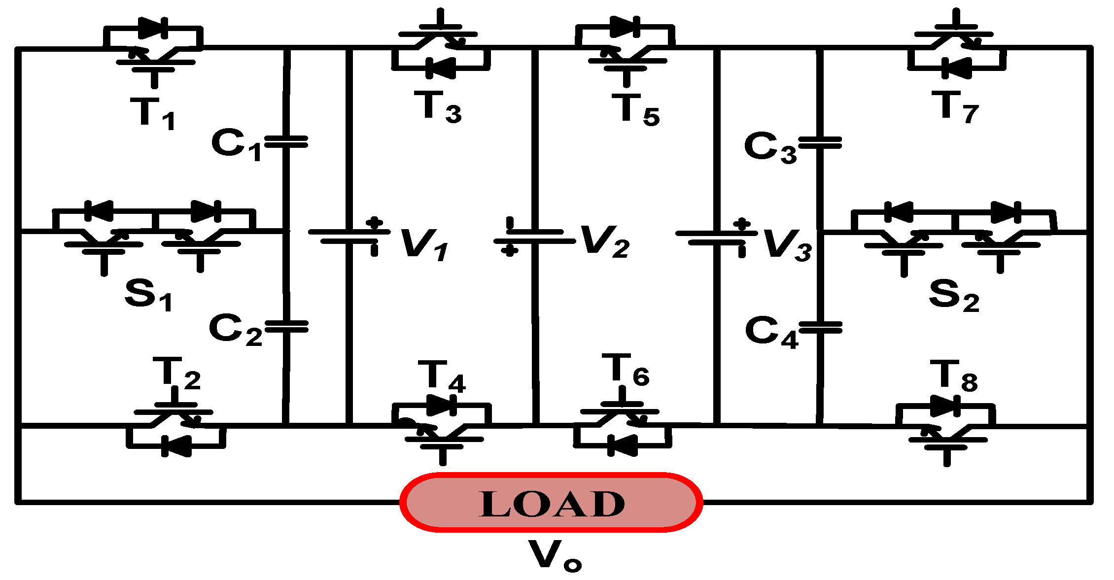
2. Proposed Topology

The description of the proposed SCMLI topology is shown in Figure 1. The circuit had eight switches (T1–T8) of unidirectional nature, three DC voltage sources, two switches (S1 and S2) that are bidirectional, and four capacitors. The switch pairs T3–T4 and T5–T6 were complementary, thus avoiding short-circuiting problems in the DC voltage supply. Similar topology works for asymmetrical and symmetrical configuration based on the intensity of V1, V2, and V3, DC voltage supplies.

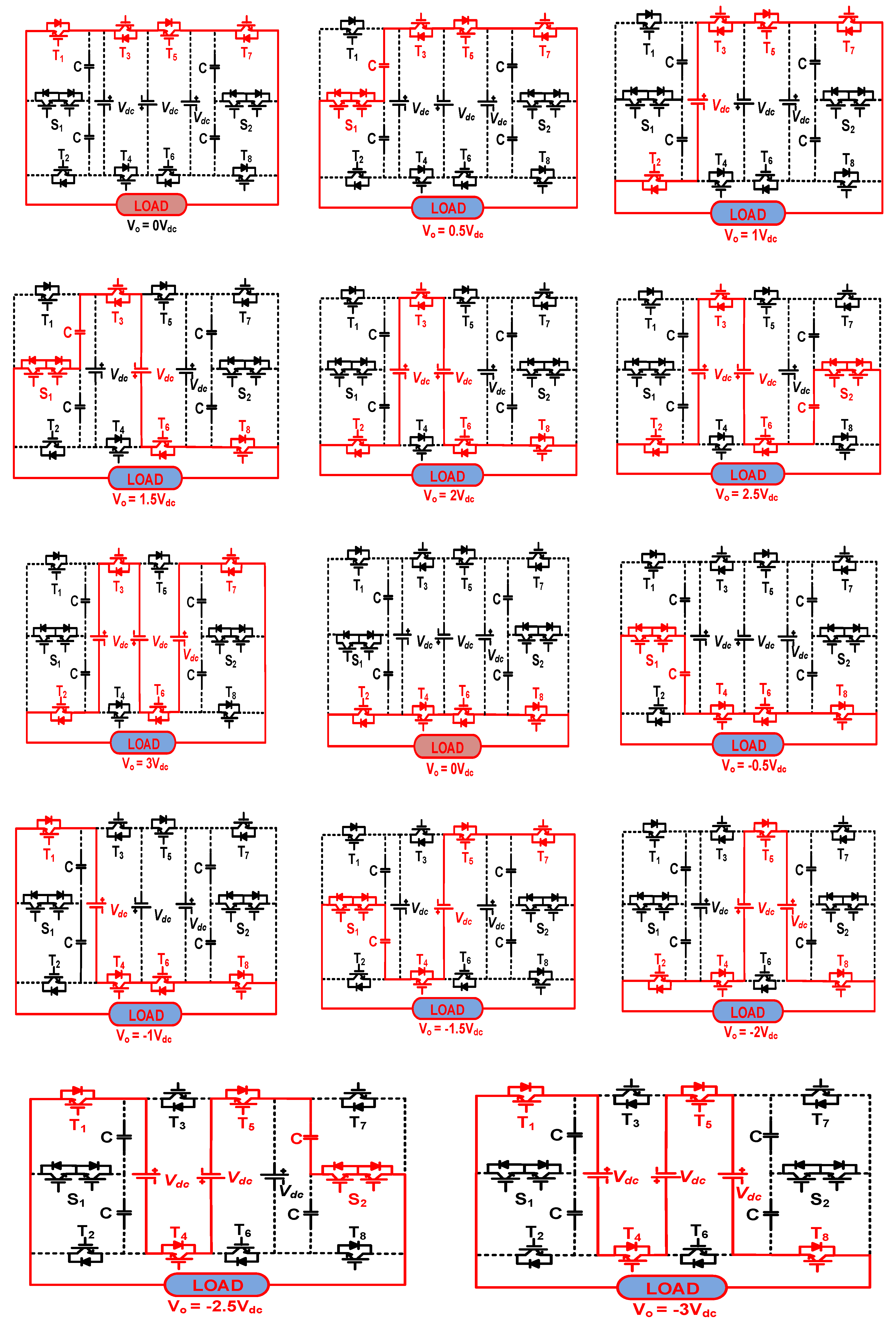
2.1. Symmetrical Configuration

For this configuration, all the sources (V1, V2, and V3) of DC voltage have the same magnitude, i.e., V1 = V2 = V3 =   V d c . Therefore, the proposed topology with symmetric configuration can generate 13 levels at the output (six positives, six negative, and zero). All the switching states of this configuration are shown in Table 1. The switching diagrams for all the thirteen switching states are shown in Figure 2. In the switching description, the undotted line indicates the active circuit having current flow. The voltage across C1 and C2 will be half of the voltage V1, and voltage across C3 and C4 will be half of the voltage V3. Total standing voltage (TSV) is a parameter that was essential for inverter configuration selection. It is the sum of the absolute maximum blocking voltages through each switch. Also, there will be the same voltage stress for complementary switches. Therefore, according to the basic circuit given in Figure 1, voltage stresses across the switches:
Switches, T1 and T2,
V S 1 = V S 2 = V 1 = V d c
Complementary switches, T3 and T4,
V S 3 = V S 4 = V 1 + V 2 = 2   V d c
Complementary switches, T5 and T6,
V S 5 = V S 6 = V 2 + V 3 = 2 V d c
Switches,
V S 7 = V S 8 = V 3 =   V d c
For bidirectional switches, each unidirectional switch of S1 and S2 had to block the voltage of both switches of bidirectional switch S1,
V S 1 = V 1 = V d c
Both switches of bidirectional switch S2,
  V S 2 = V 3 =   V d c
Therefore,
T S V = V S 1 + V S 2 + V S 3 + V S 4 + V S 5 + V S 6 + V S 7 + V S 8 + 2 V S 1 + 2 V S 2
(2 is for the 2 bidirectional switches S1 and S2).
Using Equations (1) to (6) in Equation (7), we have
T S V = 2 ( V S 1 + V S 3 + V S 5 + V S 7 + V S 1 + V S 2 ) = 2 (   V d c + 2   V d c + 2   V d c +   V d c + V d c +   V d c ) = 16   V d c
For per unit TSV, the TSV is divided by the peak of the output voltage. Therefore,
T S V p . u = 16   V d c   6   V d c = 2.67

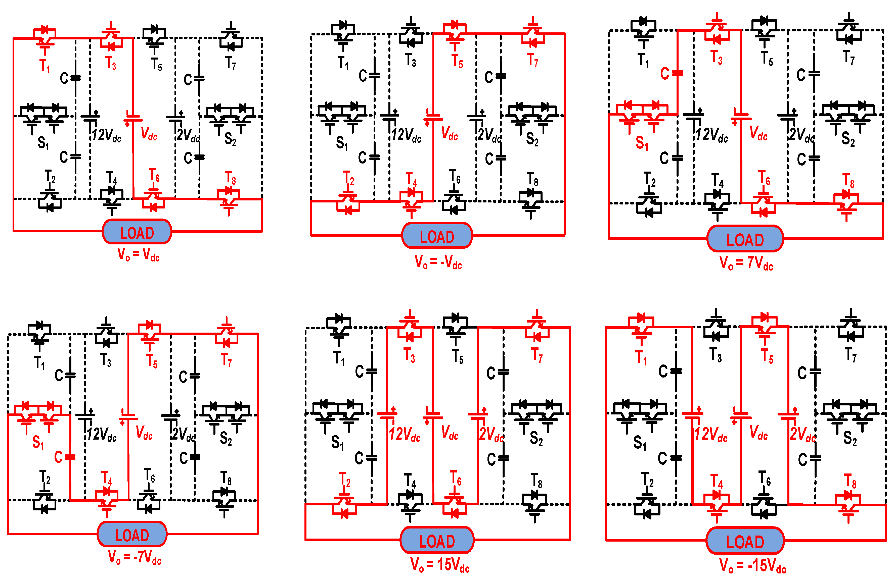
2.2. Asymmetrical Configuration

The same topology can generate more output levels using asymmetrical configuration. However, determining the appropriate ratio of the voltage sources to have maximum output levels was essential for lowering down the THD. After analyzing the combinations for the three DC voltage sources, the one with V1 = 12   V d c , V2 =   V d c , and V3 = 2 V d c gave the highest number of output levels. Thirty-one output levels can be obtained using this combination of supply of DC voltage for the same topology. Table 2 shows distinct states of switching for the configuration. The switching diagrams for some of the 31 switching states are shown in Figure 3. Voltage stresses across the switches:
V S 1 = V S 2 = V 1 = 12   V d c
V S 5 = V S 6 = V 2 + V 3 = 3   V d c
V S 7 = V S 8 = V 3 = 2   V d c
For bidirectional switches, each unidirectional switch of S1 has to block the voltage of
V S 1 = V 1 = 12 V d c
and, each unidirectional switch of S2 has to block the voltage of
V S 2 = V 3 =     2 V d c
Trefore,
T S V = 2 ( V S 1 + V S 3 + V S 5 + V S 7 + V S 1 + V S 2 )
Using Equations (10) to (15) in Equation (16), we have
T S V = 2 ( 12   V d c + 13   V d c + 3   V d c + 2   V d c + 12 V d c +   2 V d c ) = 88   V d c
For per unit TSV,
T S V p . u = 88   V d c   15   V d c = 5.87

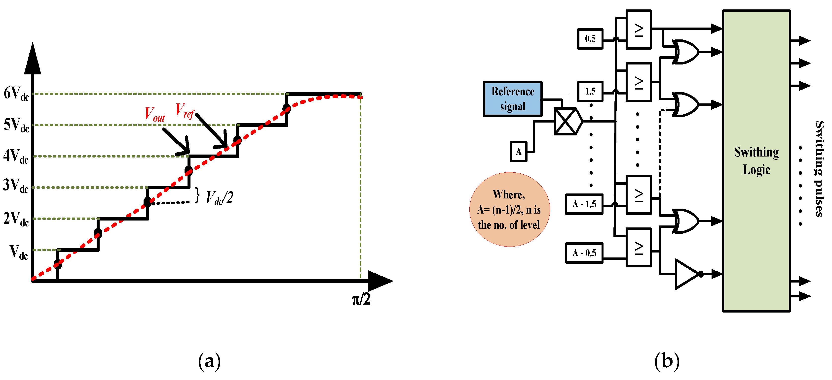
3. Nearest Level Control

Modulation techniques are of great importance for multilevel inverters as they influence harmonics, control dynamics, switching loss, filter size, etc. [38]. Traditional modulation methods have the standard features of high switching loss, switching harmonics, increased switching frequency, and high complexity as submodules increases, etc. Nearest level control (NLC) has the advantage of having more voltage levels as it approximates the reference voltage with the nearest voltage level, which results in fundamental switching frequency having low switching losses [39]. This method was useful for higher output voltage applications as the switching losses and low-order harmonics were minimized. This method can operate at 50 Hz and is extendable to N-Levels. This method was more straightforward, and the round-off method was used for the calculation of normalized value. The amplified signal was obtained by multiplying the reference signal by A, as given in Figure 4b. After comparing the signals obtained with constants, the pulses thus obtained were combined according to logic for switching to get the required pulses of switching. NLC was applied for controlling the voltage at the output of the proposed multilevel inverter for both symmetric and asymmetric configurations. The working principle of the NLC is mentioned as part of Figure 4a,b. There was a variation in the reference voltage (Vref) to change the modulation index (MI), which is given as:
Modulation   Index = V r e f V o u t = 2 V r e f ( N 1 ) V d c

4. Comparative Analysis

In this section, the SCMLI proposed is compared with the formerly presented SCMLIs. A thorough comparison was carried out considering   T S V p . u ; the number of components required; cost function (CF), which is taken from [7]; etc. Estimation of the overall cost of each topology was done using the ratio of cost function over the output voltage levels.
C F = ( N s w + N d r + N c a p + N d i +   γ   T S V p u ) × N V d c
where, N s w   represents the switch count, N d r   represents gate drivers’ count, N c a p   represents the number of capacitors, N d i   represents the diode count, N V d c   represents the number of dc voltage sources, γ represents weight coefficient, T S V p u   represents total standing voltage.
Different components required, such as gate drivers, switches, capacitors, diodes, and isolated sources of DC voltage and total standing voltage per unit, were suitably considered for the estimation of the cost function. For selecting proper switches for any topology, the TSV of the structure will be necessary. A weight coefficient (γ) was multiplied with T S V p u to precisely apply its impact on the proposed CF. γ greater than or less than one selects which among TSV and the number of switches was the most relevant quantity. The comparative analysis is done in the following two sections.

4.1. Comparision with a Single Source and Symmetric Topologies

Here, the general features of the proposed 13-level symmetric topology are compared with some recent topologies of SCMLIs and are summarized in Table 3. One of the notable merits of the proposed structure was its lowest T S V p u among the papers presented in [7,33,34,35,36,37,40,41,42]. It also had the lowest number of switch count among its 13-level counterparts. Value of C . F N l e v e l was also low for both conditions of γ = 0.5 and γ = 1.5 for 13 levels. Value of C . F N l e v e l was very high in [33,36] as compared to the proposed topology. Structures in [7,40] had a lower value of C . F N l e v e l than the proposed one as they have a single DC source, and their TSV was higher.

4.2. Comparison with a Symmetric Topologies

Asymmetric topologies have come into the picture for obtaining output levels in higher numbers. The proposed asymmetric topology was compared with recent SCMLIs of similar voltage levels comprehensively, which is shown in Table 4. For higher levels (here 31), this topology did not have a marked difference in the different properties given in the table. The value of C . F N l e v e l in the proposed MLI wass less than the structures presented in [23,43]. The number of drivers and switch count used here was lowest. Most importantly, the same topology was used for symmetric as well as asymmetric design in the topology proposed.

5. Power Loss Analysis

Losses in terms of power and efficiency in the overall sense of suggested topology were estimated by using PLECS software. Conduction and switching losses for all the switches and losses across the capacitors were calculated precisely using thermal modeling in the software. IGBT switch IGA30N60H3 manufactured by Infineon was taken for this analysis. The turn ON, turn OFF, and conduction loss model of the IGBT taken is given in Figure 5, respectively. Here three main types of losses were taken into account: switching losses ( P S ) and conduction losses ( P C ) of all the semiconductor devices and ripple loss ( P R ) of the capacitors.

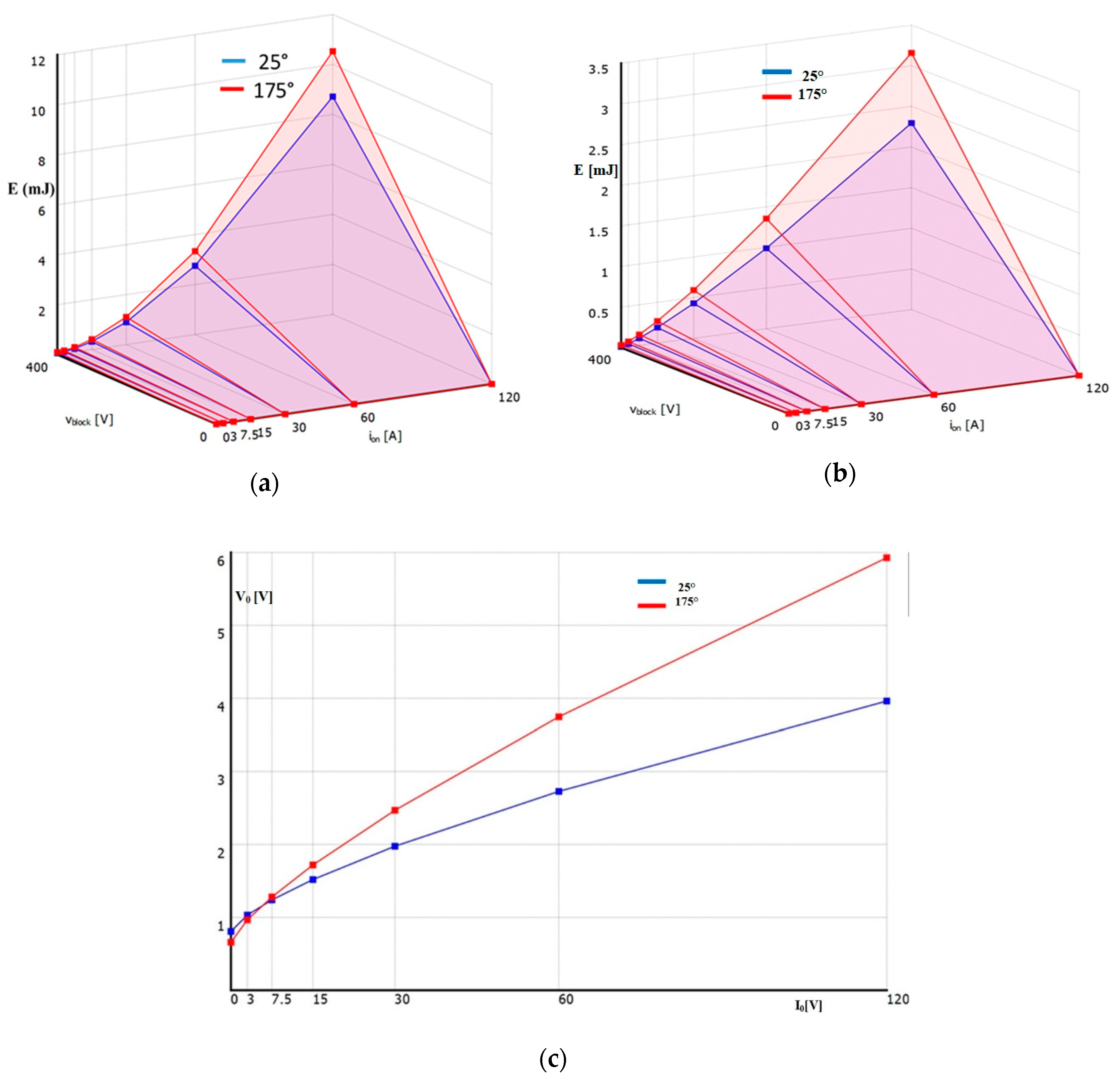
5.1. Switching Losses ( P S )

Switching losses were there at the instant when the switches turn ON or OFF. The following equations can be expressed for the kth switch considering approximation in a linear sense between current and voltage of switches during the period of switching [45]:
Loss of power during switching
ON =   P S , o n , k = f 0 t o n v ( t ) i ( t ) d t = f 0 t o n ( V S , k t o n t ) ( I k t o n ( t t o n ) ) d t =   1 6   f   V S , k I k t o n
Loss of power during switching
OFF   =   P S , o f f , k = f 0 t o f f v ( t ) i ( t ) d t = f 0 t o f f ( V S , k t o f f t ) ( I k t o f f ( t t o f f ) ) d t =   1 6   f   V S , k I k t o f f
where I k and I k denote currents across the kth switch when it was turned ON, and prior to turning it OFF, respectively. f is the frequency of switching and V S , k denotes voltage for the OFF-state of the kth switch. For calculating the loss in switching as total, the ON ( N o n ) and the OFF number of switching states ( N o f f ) for each cycle are multiplied with (21) and (22) following (23):
P S =   k = 1 12 ( m = 1 N o n P S , o n , k m + m = 1 N o f f P S , o f f , k m )

5.2. Conduction Losses ( P C )

The internal resistance of each component, i.e., semiconductor devices and capacitors, had to be addressed to calculate losses in conduction at the condition of steady-state. Each capacitor was assumed to be the same. The results were taken using the PLECS software for a resistive load since the state of resistive loading is said to be the worst-case scenario in the analysis of loss of power for the SCMLIs [45,46].

5.3. Capacitor Ripple Losses ( P R )

Ripple losses occured by the difference between the input voltage (Vin) and the voltage across the capacitors (VCj(j = 1,2,3,4)), when the capacitors are connected in parallel [46]. It was assumed that the capacitor was fully charged to Vin during the charging state.
The capacitor ripple voltage is taken as:
Δ V C j = 1 C j t t i C j ( t ) d t   for   j = 1 , 2 , 3 , 4
Here, i C j denotes passing current of the jth capacitor. The discharging period is [ t t ]. Thus, the total ripple loss in the duration of the output waveform cycle is given by (25).
P R =   f 2 j = 1 4 C j   Δ V C j 2
From (24) and (25), it is evident that ripple loss is inversely proportional to the capacitance. Thus, larger capacitance led to less ripple loss and hence improved efficiency. The efficiency of the overall proposed inverter is given by (26).
η = P o P o + P S + P C + P R
The efficiency versus output power curve for both symmetrical and asymmetrical configurations is shown in Figure 6 for a resistive load. Maximum efficiency was achieved with about 98.7% along with a 100-watt output power for both the configurations in which capacitor ripple loss had neglected. Capacitor ESR loss (conduction loss due to internal resistance of the capacitors (here 0.1 ohm is taken)) was taken in its place. Power loss distribution among different switches and capacitors are given in Figure 7 for both settings. S1 and S2 were the bidirectional switches, as shown in Figure 1. Both switches of the bidirectional switches had the same loss. All the complementary switches also had the same losses as the number of states when they were turned ON and turned OFF for a full cycle.

6. Results and Discussions

Simulation of the suggested topology for asymmetric and the symmetric case was done using Matlab ® 2018a and for verifying the results obtained, experimental results were also taken. Both of these results are discussed in the subsequent subsection.

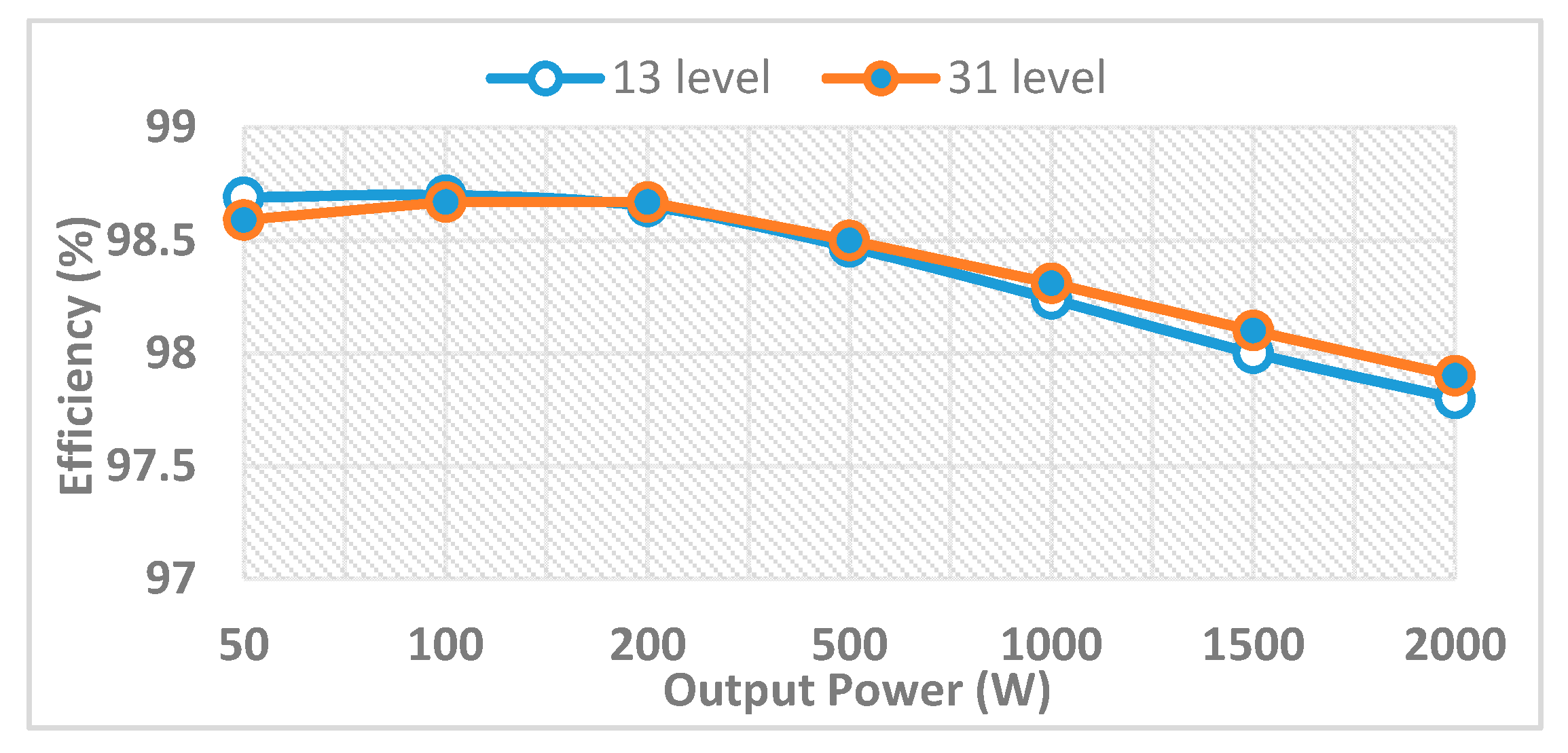
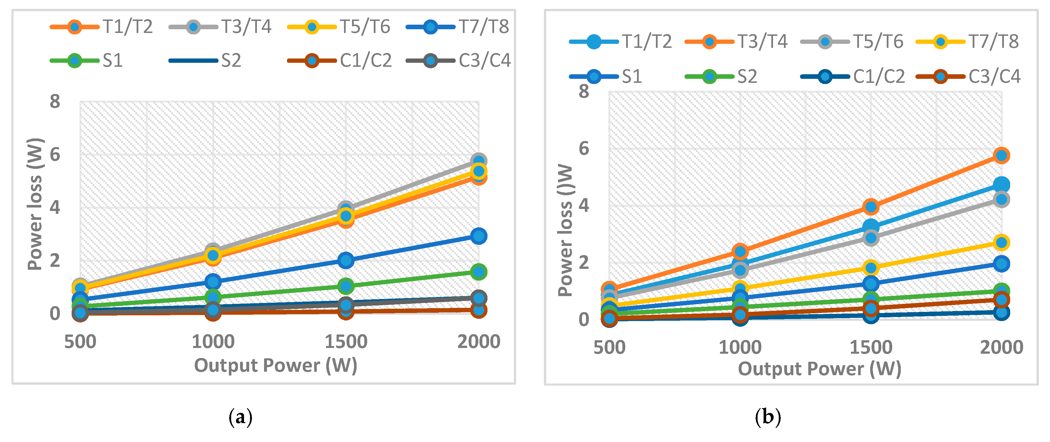
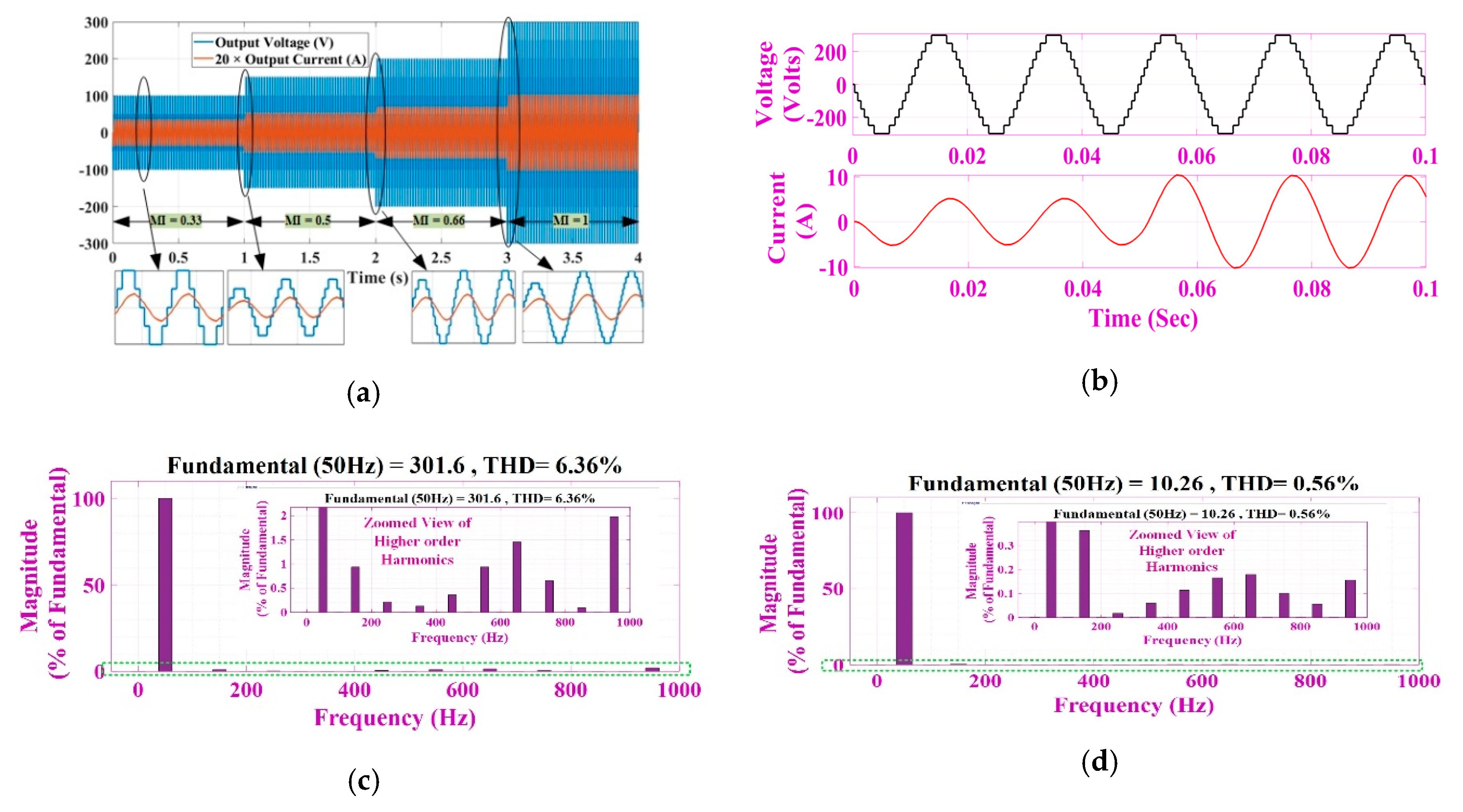
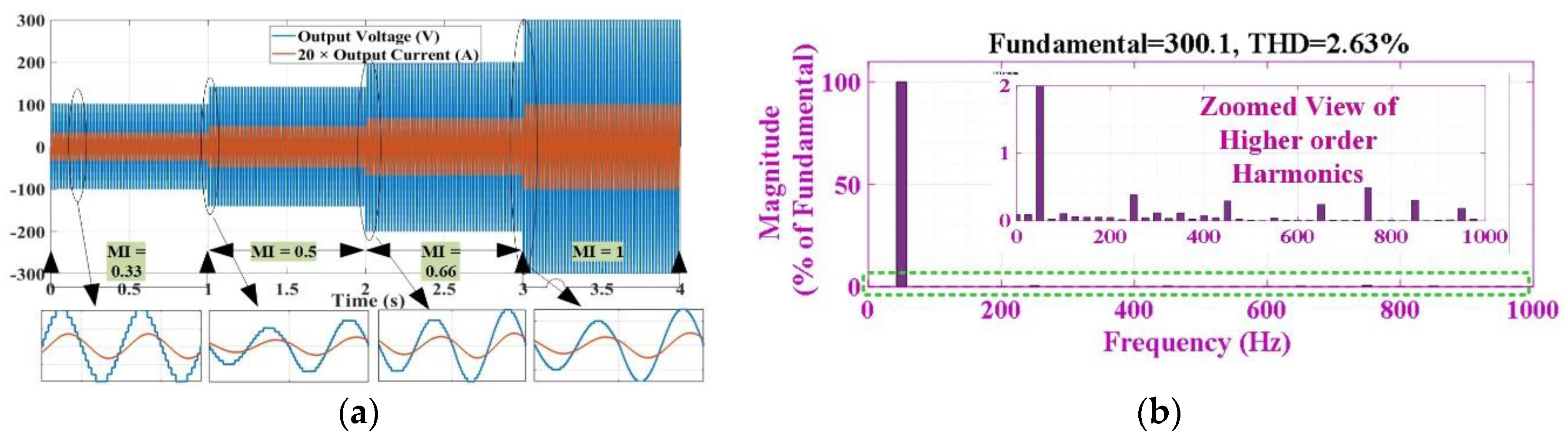
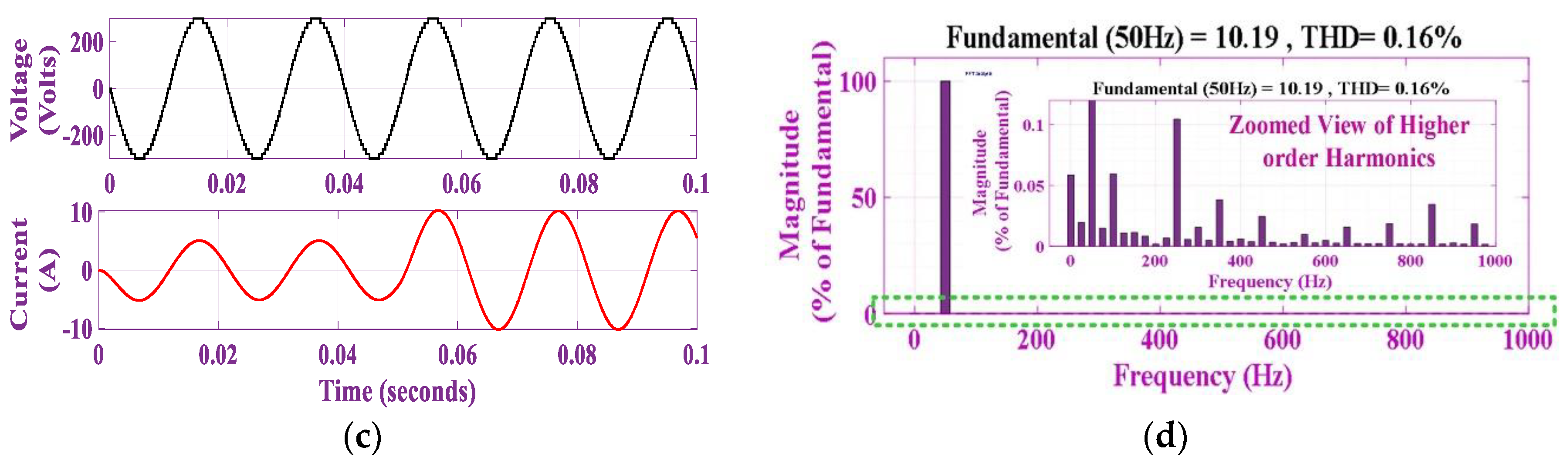
6.1. Simulation Results

For symmetrical configuration, the magnitude of the three DC voltage sources was similar, and for simulation purposes, it was taken to be 100 volts. The resultant voltage at the output had a peak voltage of 300 V with 50-V steps and 13 levels in totality. All four capacitances were considered to be 4700 µF. The current waveform and voltage at the output for Z = 50 Ω +100 mH as the R-L load with varying MI are presented in Figure 8a. The number of levels for voltage at the output was directly proportional to the MI. At MI = 0.5, the output voltage levels were reduced by half, which can be analyzed from Figure 8a. The current waveform and voltage at the output with a load change of Z = 50 Ω +100 mH to Z=25 Ω +100 mH, which are given in Figure 8b–d, show the harmonic analysis of the voltage obtained and the current waveforms for Z = 50 Ω +100 mH, respectively. Voltage and current THD was achieved as 6.36% and 0.56%, respectively. Current THD was lower as the inductive load reduced the high-frequency current components.
For the asymmetrical case, V1 = 240 V, V2 = 20 V, and V3 = 40 V. The resultant output waveform has a peak voltage of 300 Volts with a step size of 20 Volts. Figure 9a shows the current waveform and voltage at the output for Z = 50 Ω +100 mH as the R-L load with varying MI. Figure 9b presents the current waveform and voltage at the output with Z = 50 Ω +100 mH to Z = 25 Ω +100 mH as the change in load. Harmonic analysis for the obtained voltage and current waveforms for Z = 50 Ω +100 mH, as shown in Figure 9c,d, respectively. Voltage and current THD was obtained as 2.63% and 0.16%, respectively.

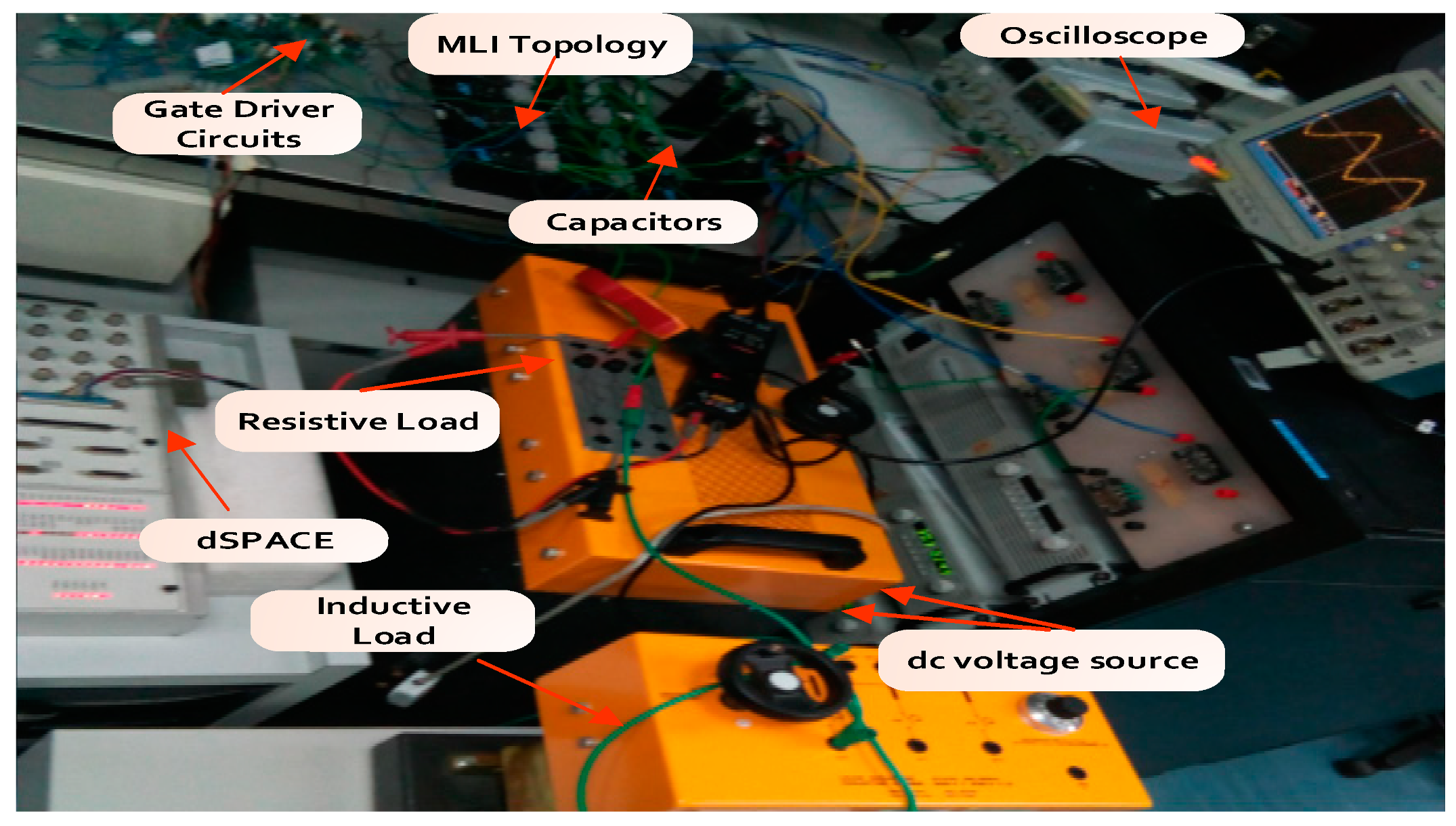
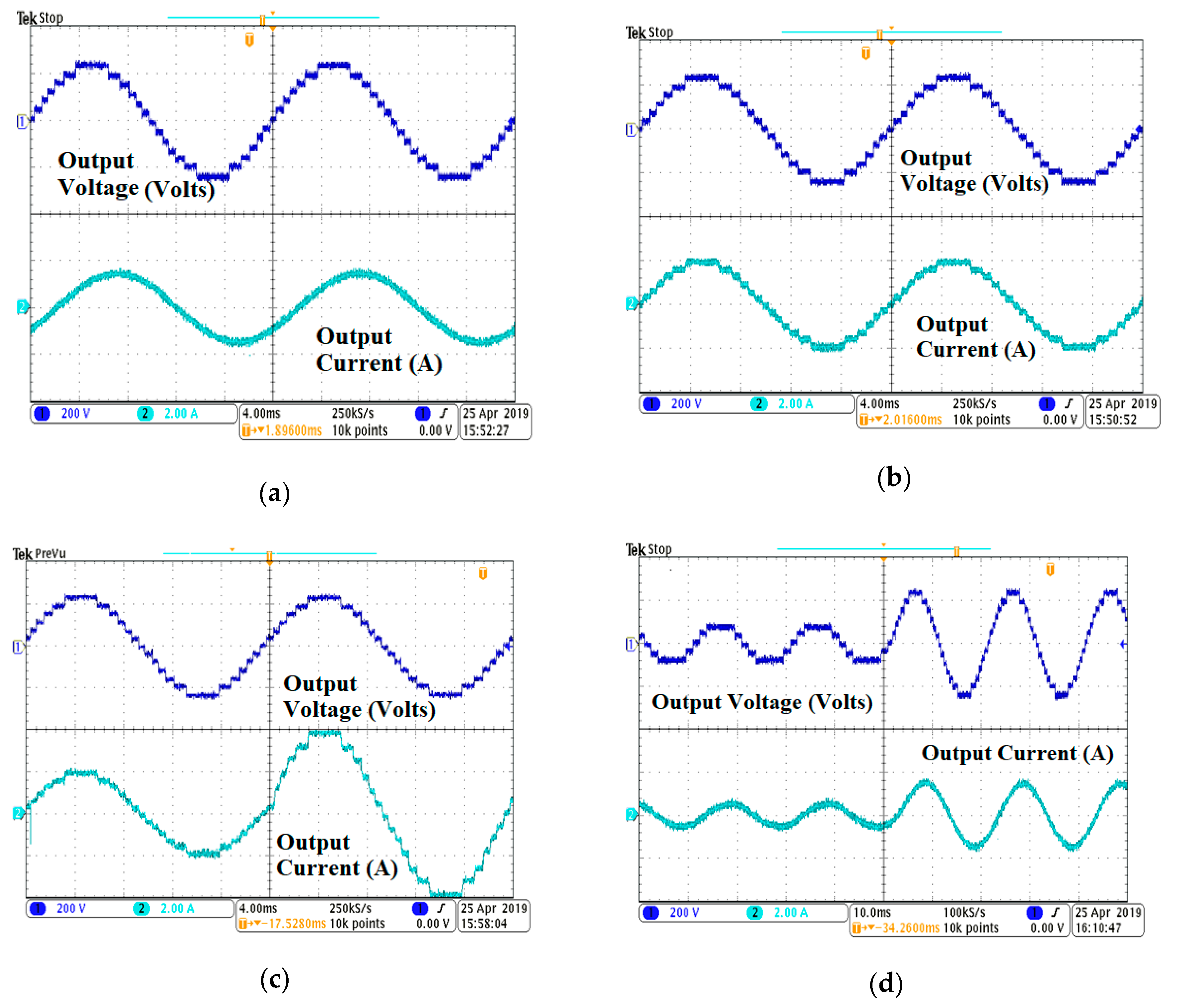
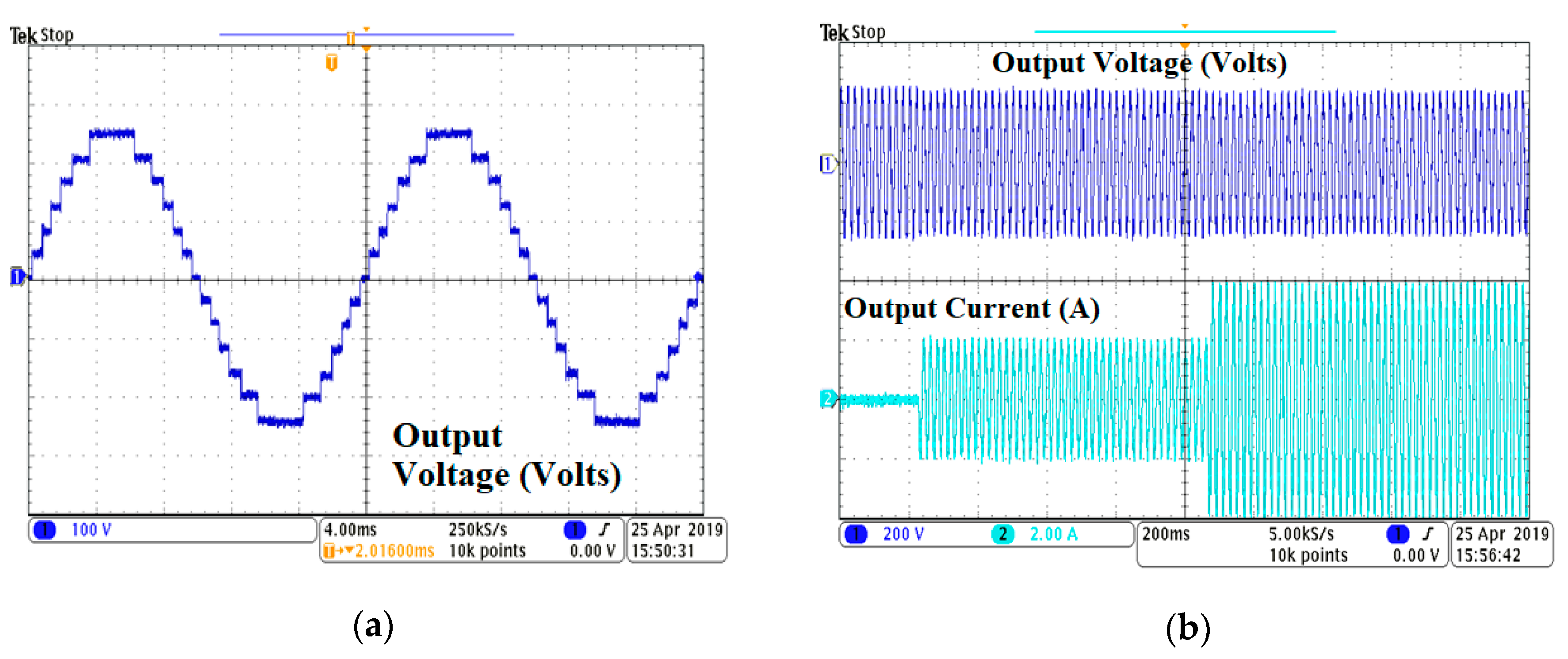
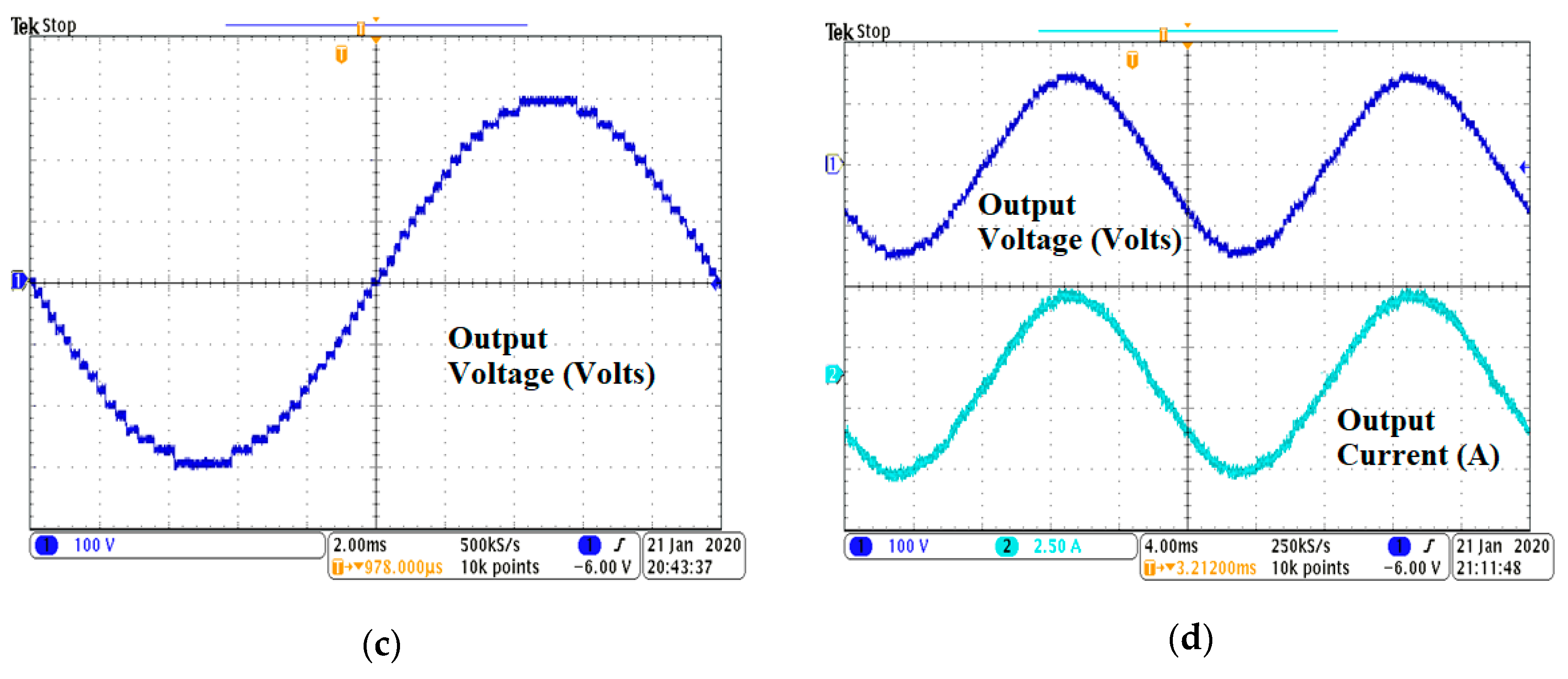
6.2. Experimental Results

Figure 10 shows that the above results obtained were verified using an experimental prototype for both symmetrical and asymmetrical cases. Toshiba IGBT GT50J325 was taken as the switch, and the dSPACE 1104 controller was used to obtain gating pulses for these switches. Figure 11a,b shows the output voltage and current waveforms for RL load of 200 Ω +100 mH and a resistive load of 120 Ω, respectively, for the symmetrical case. In this case, V1 = V2 = V3 = 80 V was chosen. The thirteen-level output had the peak voltage of 240 V with a step voltage of 40 V. The output waveforms with load change and MI change are given in Figure 11c,d. The load change was from 120 Ω to 60 Ω, and MI change was from 0.33 to 1. The 13-level output is shown in Figure 12a. For the asymmetrical case, V1 = 240 V, V2 =20 V, and V3 = 40 V were taken. Figure 12b shows the output waveform having a load change from no load to 120 Ω to 60 Ω. Figure 12c shows the thirty-one-level output voltage with the maximum voltage of 300 volts having steps of 20 volts. The output waveform for a resistive load of 32 Ω is given in Figure 12d.

7. Conclusions

An innovative SCMLI topology is suggested here. The mentioned topology could operate for symmetrical as well as the asymmetrical case. Apart from lower switch count, TSV was also remarkably lower for the symmetrical case and comparable with other recent topologies in the asymmetrical case. It had the lowest switch count compared to other 13-level topologies presented, as discussed in Section 4.1 and given in Table 3. Its economic aspect was also taken into account using the cost function, and it stands well with other topologies shown in Table 3 and Table 4. Hardware implementation was carried out to verify the simulation results under the condition of varying load and modulation indexes. Thus, the proposed topology is the right candidate to be used in the smart grid system 4.0, which has a stringent requirement under IEEE 1547 standards.

Author Contributions

Conceptualization, M.D.S. and S.A.; format analysis, M.R.H.; funding acquisition, S.A.; investigation, M.R.H., A.S., M.S., M.Z. and M.F.; methodology, A.S., M.D.S. and S.M.; project administration, S.M., S.A. and M.Z.; resources, M.D.S. and S.M.; supervision, A.S. and S.M.; validation, M.R.H., A.S., S.M., S.A., M.S., M.Z., and M.F.; visualization, M.D.S.; writing: original draft, M.R.H.; writing: review and editing, A.S., S.A., M.S., M.Z., and M.F. All authors have read and agreed to the published version of the manuscript.

Funding

The authors extend their appreciation to the Deputyship for Research & Innovation, “Ministry of Education” in Saudi Arabia for funding this research work through the project number IFKSURG-1438-089.

Conflicts of Interest

The authors declare no conflict of interest.

References

  1. Rodríguez, J.; Leon, J.I.; Kouro, S.; Portillo, R.; Prats, M.A.M. The age of multilevel converters arrives. IEEE Ind. Electron. Mag. 2008, 2, 28–39. [Google Scholar]
  2. Wang, C.; Zhu, Y.; Shi, W.; Chang, V.; Vijayakumar, P.; Liu, B.; Mao, Y.; Wang, J.; Fan, Y. A Dependable time series analytic framework for cyber-physical systems of IoT-based smart grid. ACM Trans. Cyber-Phys. Syst. 2018, 3, 1–18. [Google Scholar] [CrossRef]
  3. Otuoze, A.O.; Mustafa, M.W.; Larik, R.M. Smart grids security challenges: Classification by sources of threats. J. Electr. Syst. Inf. Technol. 2018, 5, 468–483. [Google Scholar] [CrossRef]
  4. Saeedian, M.; Hosseini, S.M.; Adabi, J. Step-up switched-capacitor module for cascaded MLI topologies. IET Power Electron. 2018, 11, 1286–1296. [Google Scholar] [CrossRef]
  5. Gupta, K.K.; Ranjan, A.; Bhatnagar, P.; Sahu, L.K.; Jain, S. Multilevel inverter topologies with reduced device count: A review. IEEE Trans. Power Electron. 2016, 31, 135–151. [Google Scholar] [CrossRef]
  6. Chakraborty, C.; Iu, H.H.C.; Lu, D.D.C. Power converters, control, and energy management for distributed generation. IEEE Trans. Ind. Electron. 2015, 62, 4466–4470. [Google Scholar] [CrossRef]
  7. Barzegarkhoo, R.; Moradzadeh, M.; Zamiri, E.; Madadi Kojabadi, H.; Blaabjerg, F. A new boost switched-capacitor multilevel converter with reduced circuit devices. IEEE Trans. Power Electron. 2018, 33, 6738–6754. [Google Scholar] [CrossRef]
  8. Siddique, M.D.; Mekilef, S.; Shah, N.M.; Memon, M.A. Optimal design of a new cascaded multilevel inverter topology with reduced switch count. IEEE Access 2019, 7, 24498–24510. [Google Scholar] [CrossRef]
  9. Dargahi, V.; Sadigh, A.K.; Abarzadeh, M.; Eskandari, S.; Corzine, K. A new family of modular multilevel converter based on modified flying-capacitor multicell converters. IEEE Trans. Power Electron. 2014, 30, 138–147. [Google Scholar] [CrossRef]
  10. López, I.; Ceballos, S.; Pou, J.; Zaragoza, J.; Andreu, J.; Kortabarria, I.; Agelidis, V.G. Modulation strategy for multiphase neutral-point-clamped converters. IEEE Trans. Power Electron. 2015, 31, 928–941. [Google Scholar] [CrossRef]
  11. Zhang, Y.; Adam, G.P.; Lim, T.C.; Finney, S.J.; Williams, B.W. Hybrid multilevel converter: Capacitor voltage balancing limits and its extension. IEEE Trans. Ind. Inform. 2013, 9, 2063–2073. [Google Scholar] [CrossRef]
  12. Malinowski, M.; Gopakumar, K.; Rodriguez, J.; Perez, M.A. A survey on cascaded multilevel inverters. IEEE Trans. Ind. Electron. 2010, 57, 2197–2206. [Google Scholar] [CrossRef]
  13. Mathew, R.; Agarwal, S. Modified reduced switch symmetrical multilevel inverter. In Proceedings of the IEEE International Conference on Circuit, Power and Computing Technologies, ICCPCT 2017, Kollam, India, 20–21 April 2017; pp. 1–8. [Google Scholar]
  14. Lee, S.S.; Sidorov, M.; Idris, N.R.N.; Heng, Y.E. A symmetrical cascaded compact-module multilevel inverter (CCM-MLI) with pulsewidth modulation. IEEE Trans. Ind. Electron. 2018, 65, 4631–4639. [Google Scholar] [CrossRef]
  15. Saha, D.; Roy, T. A new symmetrical three phase multilevel inverter using switched capacitor basic units for renewable energy conversion systems. In Proceedings of the 2018 International Conference on Control, Power, Communication and Computing Technologies (ICCPCCT), Kannur, India, 23–24 March 2018; pp. 368–374. [Google Scholar]
  16. Salem, A.; Ahmed, E.M.; Ahmed, M.; Orabi, M. Stand-alone three-phase symmetrical multi-level inverter. In Proceedings of the 2015 IEEE International Telecommunications Energy Conference (INTELEC), Saka, Japan, 18–22 October 2015; pp. 1–6. [Google Scholar]
  17. Salem, A.; Ahmed, E.M.; Orabi, M.; Ahmed, M. New three-phase symmetrical multilevel voltage source inverter. IEEE J. Emerg. Sel. Top. Circuits Syst. 2015, 5, 430–442. [Google Scholar] [CrossRef]
  18. Siddique, M.D.; Alamri, B.; Salem, F.A.; Orabi, M.; Mekhilef, S.; Shah, N.M.; Sandeep, N.; Mohamed Ali, J.S.; Iqbal, A.; Ahmed, M.; et al. A single DC source nine-level switched-capacitor boost inverter topology with reduced switch count. IEEE Access 2020, 8, 5840–5851. [Google Scholar] [CrossRef]
  19. Samadaei, E.; Salehi, A.; Iranian, M.; Pouresmaeil, E. Single DC source multilevel inverter with changeable gains and levels for low-power loads. Electronics 2020, 9, 937. [Google Scholar] [CrossRef]
  20. Wang, J.; Wang, J.; Xiao, B.; Gui, Z.; Jiang, W. Full range capacitor voltage balance PWM strategy for diode-clamped multilevel inverter. Electronics 2020, 9, 1263. [Google Scholar] [CrossRef]
  21. Siddique, M.D.; Mekhilef, S.; Shah, N.M.; Sarwar, A.; Iqbal, A.; Tayyab, M.; Ansari, M.K. Low switching frequency based asymmetrical multilevel inverter topology with reduced switch count. IEEE Access 2019, 7, 86374–86383. [Google Scholar] [CrossRef]
  22. Siddique, M.D.; Mustafa, A.; Sarwar, A.; Mekhilef, S.; Shah, N.B.M.; Seyedamahmousian, M.; Stojcevski, A.; Horan, B.; Ogura, K. Single phase symmetrical and asymmetrical design of multilevel inverter topology with reduced number of switches. In Proceedings of the 2018 IEEMA Engineer Infinite Conference (eTechNxT), New Delhi, India, 13–14 March 2018; pp. 1–6. [Google Scholar]
  23. Siddique, M.D.; Mekhilef, S.; Shah, N.M.; Sarwar, A.; Iqbal, A.; Memon, M.A. A new multilevel inverter topology with reduce switch count. IEEE Access 2019, 7, 58584–58594. [Google Scholar] [CrossRef]
  24. Almakhles, D.J.; Ali, J.S.M.; Padmanaban, S.; Bhaskar, M.S.; Subramaniam, U.; Sakthivel, R. An original hybrid multilevel DC-AC converter using single-double source unit for medium voltage applications: Hardware implementation and investigation. IEEE Access 2020, 8, 71291–71301. [Google Scholar] [CrossRef]
  25. Lee, S.S. A single-phase single-source 7-level inverter with triple voltage boosting gain. IEEE Access 2018, 6, 30005–30011. [Google Scholar] [CrossRef]
  26. Ye, Y.; Cheng, K.W.E.; Liu, J.; Ding, K. A step-up switched-capacitor multilevel inverter with self-voltage balancing. IEEE Trans. Ind. Electron. 2014, 61, 6672–6680. [Google Scholar] [CrossRef]
  27. Liu, J.; Wu, J.; Zeng, J. Symmetric/Asymmetric hybrid multilevel inverters integrating switched-capacitor techniques. IEEE J. Emerg. Sel. Top. Power Electron. 2018, 6, 1616–1626. [Google Scholar] [CrossRef]
  28. Roy, T.; Bhattacharjee, B.; Sadhu, P.K.; Dasgupta, A.; Mohapatra, S. Step-up switched capacitor multilevel inverter with a cascaded structure in asymmetric DC source configuration. J. Power Electron. 2018, 18, 1051–1066. [Google Scholar]
  29. Raghu Raman, S.; Cheng, K.W.E.; Ye, Y. multi-input switched-capacitor multilevel inverter for high-frequency AC Power distribution. IEEE Trans. Power Electron. 2018, 33, 5937–5948. [Google Scholar] [CrossRef]
  30. Fong, Y.C.; Raman, S.R.; Ye, Y.; Cheng, K.W.E. Generalized topology of a hybrid switched-capacitor multilevel inverter for high-frequency AC power distribution. IEEE J. Emerg. Sel. Top. Power Electron. 2020, 8, 2886–2897. [Google Scholar] [CrossRef]
  31. Zeng, J.; Wu, J.; Liu, J.; Guo, H. A quasi-resonant switched-capacitor multilevel inverter with self-voltage balancing for single-phase high-frequency AC microgrids. IEEE Trans. Ind. Inf. 2017, 13, 2669–2679. [Google Scholar] [CrossRef]
  32. Axelrod, B.; Berkovich, Y.; Ioinovici, A. A cascade boost-switched-capacitor-converter two level inverter with an optimized multilevel output waveform. IEEE Trans. Circuits Syst. Regul. Pap. 2005, 52, 2763–2770. [Google Scholar] [CrossRef]
  33. Liu, J.; Cheng, K.W.E.; Ye, Y. A cascaded multilevel inverter based on switched-capacitor for high-frequency AC power distribution system. IEEE Trans. Power Electron. 2014, 29, 4219–4230. [Google Scholar] [CrossRef]
  34. Alishah, R.S.; Hosseini, S.H.; Babaei, E.; Sabahi, M.; Zare, A. Extended high step-up structure for multilevel converter. IET Power Electron. 2016, 9, 1894–1902. [Google Scholar] [CrossRef]
  35. Roy, T.; Sadhu, P.K.; Dasgupta, A. Cross-switched multilevel inverter using novel switched capacitor converters. IEEE Trans. Ind. Electron. 2019, 66, 8521–8532. [Google Scholar] [CrossRef]
  36. Babaei, E.; Kangarlu, M.F.; Mazgar, F.N. Symmetric and asymmetric multilevel inverter topologies with reduced switching devices. Electr. Power Syst. Res. 2012, 86, 122–130. [Google Scholar] [CrossRef]
  37. Taghvaie, A.; Adabi, J.; Rezanejad, M. A self-balanced step-up multilevel inverter based on switched-capacitor structure. IEEE Trans. Power Electron. 2018, 33, 199–209. [Google Scholar] [CrossRef]
  38. Wu, D.; Peng, L. Characteristics of nearest level modulation method with circulating current control for modular multilevel converter. IET Power Electron. 2016, 9, 155–164. [Google Scholar] [CrossRef]
  39. Kouro, S.; Bernal, R.; Miranda, H.; Silva, C.A.; Rodríguez, J. High-performance torque and flux control for multilevel inverter fed induction motors. IEEE Trans. Power Electron. 2007, 22, 2116–2123. [Google Scholar] [CrossRef]
  40. Saeedian, M.; Adabi, M.E.; Hosseini, S.M.; Adabi, J.; Pouresmaeil, E. A novel step-up single source multilevel inverter: Topology, operating principle, and modulation. IEEE Trans. Power Electron. 2019, 34, 3269–3282. [Google Scholar] [CrossRef] [Green Version]
  41. Gautam, S.P.; Kumar, L.; Gupta, S. Hybrid topology of symmetrical multilevel inverter using less number of devices. IET Power Electron. 2015, 8, 2125–2135. [Google Scholar] [CrossRef]
  42. Babaei, E.; Gowgani, S.S. Hybrid multilevel inverter using switched capacitor units. IEEE Trans. Ind. Electron. 2014, 61, 4614–4621. [Google Scholar] [CrossRef]
  43. Alishah, R.S.; Hosseini, S.H.; Babaei, E.; Sabahi, M. Optimal design of new cascaded switch-ladder multilevel inverter structure. IEEE Trans. Ind. Electron. 2017, 64, 2072–2080. [Google Scholar] [CrossRef]
  44. Taheri, A.; Rasulkhani, A.; Ren, H.-P. An asymmetric switched capacitor multilevel inverter with component reduction. IEEE Access 2019, 7, 127166–127176. [Google Scholar] [CrossRef]
  45. Zamiri, E.; Vosoughi, N.; Hosseini, S.H.; Barzegarkhoo, R.; Sabahi, M. A new cascaded switched-capacitor multilevel inverter based on improved series-parallel conversion with less number of components. IEEE Trans. Ind. Electron. 2016, 63, 3582–3594. [Google Scholar] [CrossRef]
  46. Barzegarkhoo, R.; Kojabadi, H.M.; Zamiry, E.; Vosooghi, N.; Chang, L. Generalized structure for a single phase switched- capacitor multilevel inverter using a new multiple DC link producer with reduced number of switches. IEEE Trans. Power Electron. 2016, 31, 5604–5617. [Google Scholar] [CrossRef]
Figure 1. Proposed switched-capacitor multilevel inverter (SCMLI) topology.
Electronics 09 01703 g001
Figure 2. All the thirteen switching states of the symmetrical configuration.
Electronics 09 01703 g002
Figure 3. Some of the switching states of the asymmetrical configuration.
Electronics 09 01703 g003
Figure 4. Nearest level control (NLC): (a) NLC having sampled reference voltage, (b) workings of NLC.
Electronics 09 01703 g004
Figure 5. Loss model for (a) turn ON, (b) turn OFF, and (c) conduction loss for IGBT IGA30N60H3.
Electronics 09 01703 g005
Figure 6. Efficiency versus output power curve for both symmetrical and asymmetrical configurations.
Electronics 09 01703 g006
Figure 7. Distribution of power loss for (a) symmetrical 13-level topology and (b) asymmetrical 31-level topology.
Electronics 09 01703 g007
Figure 8. Simulation results of 13-level symmetric topology with (a) dynamic change of modulation index, (b) output waveforms for varying load, (c) Harmonic profile of the output voltage for Z = 50 Ω +100 mH, and (d) Harmonic profile of the output current for Z = 50 Ω +100 mH.
Electronics 09 01703 g008
Figure 9. Simulation results of 31-level asymmetric topology with (a) dynamic change of modulation index, (b) Harmonic profile of the output voltage for Z = 50 Ω +100 mH, (c) output waveforms for varying load of Z = 50 Ω +100 mH to Z = 25 Ω +100 mH, and (d) Harmonic profile of the output current for Z = 50 Ω +100 mH.
Electronics 09 01703 g009aElectronics 09 01703 g009b
Figure 10. Experimental setup of the proposed topology.
Electronics 09 01703 g010
Figure 11. Experimental results: (a) Output voltage and current for the symmetric case with Resistive-Inductive (R-L) load; (b) output waveform with R-load; (c) output waveform with load change; (d) output waveform with Modulation Index (MI) change.
Electronics 09 01703 g011
Figure 12. Experimental results: (a) Output voltage for the symmetrical case having 13 levels; (b) output waveform with zero, R, and half of R load; (c) output voltage for the asymmetrical case having 31 levels; (d) output waveform for the asymmetrical case for resistive load.
Electronics 09 01703 g012aElectronics 09 01703 g012b
Table 1. Switching states for the symmetrical configuration.
S1S2T1T2T3T4T5T6T7T8Vo
OFFOFFONOFFONOFFONOFFONOFF0
ONOFFOFFOFFONOFFONOFFONOFF0.5 V d c
OFFOFFOFFONONOFFONOFFONOFF V d c
ONOFFOFFOFFONOFFOFFONOFFON1.5 V d c
OFFOFFOFFONONOFFOFFONOFFON2 V d c
OFFONOFFONONOFFOFFONOFFOFF2.5 V d c
OFFOFFOFFONONOFFOFFONONOFF3 V d c
OFFOFFOFFONOFFONOFFONOFFON0
ONOFFOFFOFFOFFONOFFONOFFON 0.5 V d c
OFFOFFONOFFOFFONOFFONOFFON V d c
ONOFFOFFOFFOFFONONOFFONOFF 1.5 V d c
OFFOFFONOFFOFFONONOFFONOFF 2 V d c
OFFONONOFFOFFONONOFFOFFOFF 2.5 V d c
OFFOFFONOFFOFFONONOFFOFFON 3 V d c
Table 2. Switching states for the asymmetrical configuration.
S1S2T1T2T3T4T5 T6T7T8Vo
OFFOFFOFFONOFFONOFFONOFFON0
OFFOFFONOFFONOFFOFFONOFFON V d c
OFFOFFOFFONOFFONOFFONONOFF 2 V d c
OFFOFFONOFFONOFFOFFONONOFF 3 V d c
ONOFFOFFOFFONOFFONOFFOFFON 4 V d c
ONONOFFOFFONOFFONOFFOFFOFF 5 V d c
ONOFFOFFOFFONOFFONOFFONOFF 6 V d c
ONOFFOFFOFFONOFFOFFONOFFON 7 V d c
ONONOFFOFFONOFFOFFONOFFOFF 8 V d c
ONOFFOFFOFFONOFFOFFONONOFF 9 V d c
OFFOFFOFFONONOFFONOFFOFFON 10 V d c
OFFONOFFONONOFFONOFFOFFOFF 11 V d c
OFFOFFOFFONONOFFONOFFONOFF 12 V d c
OFFOFFOFFONONOFFOFFONOFFON 13 V d c
OFFONOFFONONOFFOFFONOFFOFF 14 V d c
OFFOFFOFFONONOFFOFFONONOFF 15 V d c
OFFOFFONOFFONOFFONOFFONOFF0
OFFOFFOFFONOFFONONOFFONOFF V d c
OFFOFFONOFFONOFFONOFFOFFON 2 V d c
OFFOFFOFFONOFFONONOFFOFFON 3 V d c
ONOFFOFFOFFOFFONOFFONONOFF 4 V d c
ONONOFFOFFOFFONOFFONOFFOFF 5 V d c
ONOFFOFFOFFOFFONOFFONOFFON 6 V d c
ONOFFOFFOFFOFFONONOFFONOFF 7 V d c
ONONOFFOFFOFFONONOFFOFFOFF 8 V d c
ONOFFOFFOFFOFFONONOFFOFFON 9 V d c
OFFOFFONOFFOFFONOFFONONOFF 10 V d c
OFFONONOFFOFFONOFFONOFFOFF 11 V d c
OFFOFFONOFFOFFONOFFONOFFON 12 V d c
OFFOFFONOFFOFFONONOFFONOFF 13 V d c
OFFONONOFFOFFONONOFFOFFOFF 14 V d c
OFFOFFONOFFOFFONONOFFOFFON 15 V d c
Table 3. Comparison of the proposed symmetric topology with different single source and symmetric topologies of similar voltage levels.
SCMLI Presented in N l e v e l N s w N V d c N d r N c a p N d i T S V p u C . F N l e v e l
γ = 0.5γ = 1.5
[7] sym91018216.002.703.33
[7] asym1718214426.004.825.52
[33]1318318335.0010.2711.42
[34]1314214445.305.956.76
[35]1316216425.606.277.13
[36]1314614004.7013.1116.20
[37]1329129504.835.035.40
[40]9818444.002.903.33
[41]1714414484.259.9110.91
[42]1710210245.503.384.03
Proposed multilevel inverters (MLI)1312310402.176.086.75
Table 4. Comparison of the proposed asymmetric topology with asymmetric topologies of similar voltage levels.
SCMLI Presented in N l e v e l N s w N V d c N d r N c a p N d i T S V p u C . F N l e v e l
γ = 0.5γ = 1.5
[34]3114214445.332.492.83
[35]3116216425.672.633.00
[42]2512212225.002.442.84
[43]3114610005.335.166.19
[23]2512410005.003.924.72
[34]4918218665.502.072.30
[44]2514210405.832.472.94
Proposed MLI3112310405.872.803.37
Publisher’s Note: MDPI stays neutral with regard to jurisdictional claims in published maps and institutional affiliations.

