Low Phase Noise and Wide-Range Class-C VCO Using Auto-Adaptive Bias Technique


Department of Electrical and Engineering, Chung-Ang University, Seoul 06974, Korea
*
Author to whom correspondence should be addressed.
Electronics 2020, 9(8), 1290; https://doi.org/10.3390/electronics9081290
Submission received: 2 July 2020
/
Revised: 7 August 2020
/
Accepted: 8 August 2020
/
Published: 11 August 2020
(This article belongs to the Special Issue 5G Front-End Transceivers)
Abstract
:This paper proposes a new structure of 24-GHz class-C voltage-controlled oscillator (VCO) using an auto-adaptive bias technique. The VCO in this paper uses a digitally controlled circuit to eliminate the possibility of start-up failure that a class-C structure can have and has low phase noise and a wide frequency range. To expand the frequency tuning range, a 3-bit cap-bank is used and a triple-coupled transformer is used as the core inductor. The proposed class-C VCO implements a 65-nm RF CMOS process. It has a phase noise performance of −105 dBc/Hz or less at 1-MHz offset frequency and the output frequency range is from 22.8 GHz to 27.3 GHz, which consumes 8.3–10.6 mW of power. The figure-of-merit with tuning range (FoMT) of this design reached 191.1 dBc/Hz.
Keywords:
RF; CMOS; Class-C; voltage-controlled oscillator (VCO); auto-adaptive bias; phase noise; wide-range1. Introduction
Voltage-controlled oscillator (VCO) is a fundamental component used in communication systems requiring a frequency synthesizer. VCO with high output frequency is mainly used in 5G communication system or sensor system. In VCO design, there are four main factors that affect performance—power consumption, phase noise, output frequency and its range. Among these, phase noise is the most important factor in VCO performance. Therefore, design efforts should be made in the direction of improving the phase noise of the oscillator [1,2,3,4,5,6,7,8,9].
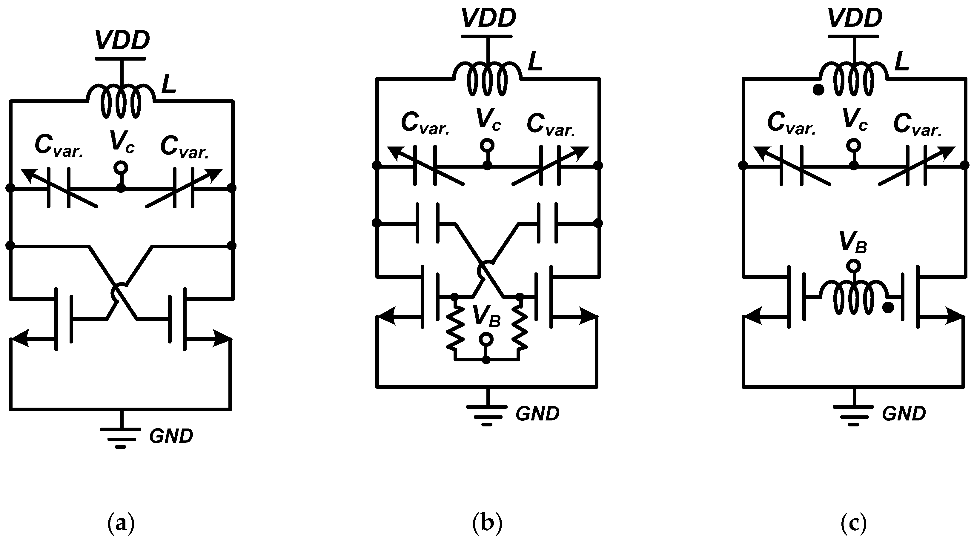
Figure 1 shows the structure of the LC VCO. It is an oscillation circuit that receives the input of the control voltage VC and determines the output frequency with the center tap inductor L and varactor Cvar. Figure 1a is a classical class-B VCO using a structure that differentially cross-couples two NMOSs. And the basic structure of class-C VCO is shown in Figure 1b. Since the gate bias voltage, VB, of the core transistor NMOS must be provided independently, it adds a capacitor to the core to cut the DC. Figure 1c is a class-C VCO using a transformer structure using an inductor without using a relatively large capacitor. Again, VB is provided independently.
The phase noise shows a sensitive characteristic in the zero-crossing point of the waveform of the VCO. Class-C VCO can improve the phase noise performance by reducing the gate bias of the cross-coupled NMOS and shortening the time passing through the zero-crossing point by giving the current flowing in the drain in a pulse shape [2,5].
The class-C VCO achieves about 2 dB to 4 dB lower phase noise than the typical class-B VCO at the same power dissipation [6,10]. However, there are two major design issues, as the class-C VCO is well known in previous works. One is that VCO start-up problems can occur and the other is how to control the gate bias of the core transistor, which determines phase noise when the VCO oscillates at the target frequency. If the gate bias of the core transistor NMOS is lowered in the class-C VCO, the transconductance is affected and the VCO fails to start operation. In order to solve the start-up problem, methods have been proposed to alleviate the initial oscillation condition in class-C mode. The class-B/C hybrid VCO is a class-B cross-coupled pair added to the class-C core [11,12]. The VCO is easily oscillated by the class-B core and the oscillation is maintained by the class-C core after the initial oscillation. However, the parasitic capacitance of the class-B core influences the LC resonance tank, which has the disadvantage of outputting the wrong frequency. Moreover, since the gate bias voltage point of the VCO core changes when the target output frequency changes, it is difficult to find that point. So, it is not easy to design a class-C VCO with wide frequency tuning range.
Another start-up solution is to directly adjust the gate bias of the class-C core using an amplifier [13,14]. Using the output voltage of the amplifier as the gate bias, the VCO starts at the high gate bias and changes to the low gate bias corresponding to class-C. However, the use of the amplifier degrades the phase noise performance of the VCO and the stabilization time is long due to the narrow bandwidth of the analog feedback loop. In addition, the above methods set the gate bias of the class-C core depending on an externally applied reference voltage, so that the bias cannot be automatically corrected when the oscillation fails.
This paper presents a startup loop to alleviate the startup problem and sets the VCO operating in the optimal phase-noise state. And the proposed VCO is designed to provide consistent output in various PVT conditions with auto-adaptive bias technique.
2. Proposed Class-C VCO Description
2.1. Design of the Class-C VCO Core
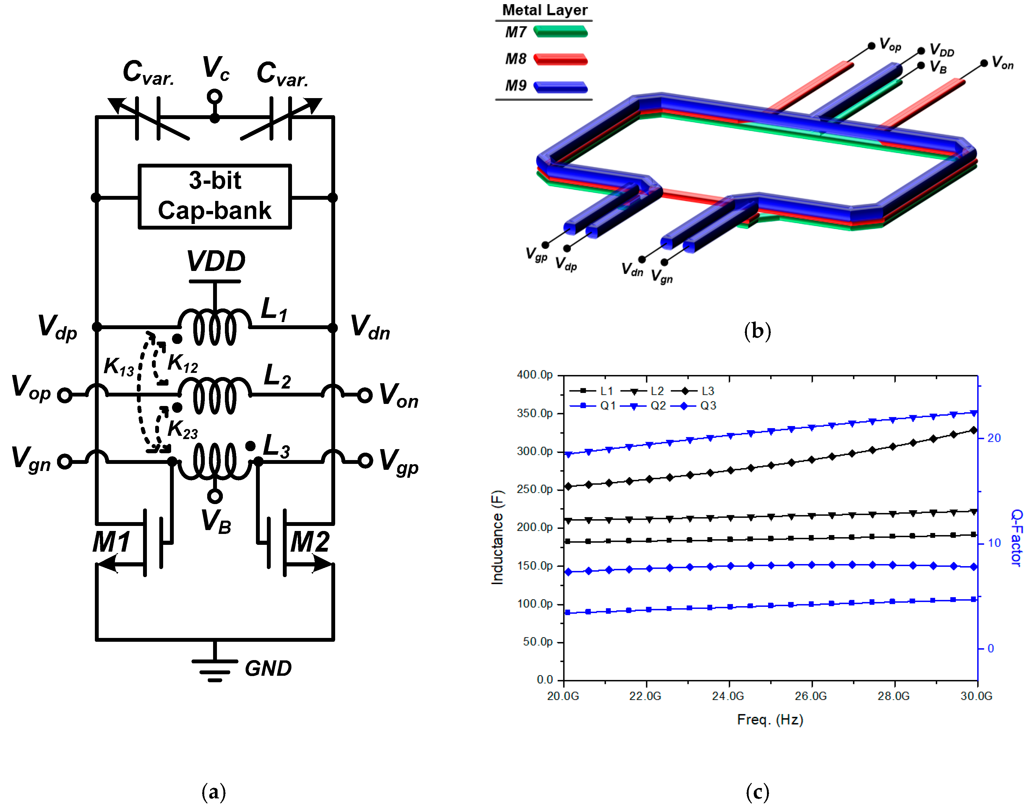
Figure 2a shows a proposed class-C VCO core, which consists of varactors, a 3-bit capacitor bank, a triple-coupled transformer and NMOS (M1, M2) cross-coupled pair. The varactor determines the slope of the output frequency according to the input voltage of the VCO (commonly referred to as KVCO). It can be seen from Leeson’s rule that the phase noise of VCO is also influenced by KVCO. KVCO and phase noise are inversely proportional but the smaller the slope, the narrower the tuning range of the VCO. The 3-bit capacitor bank is used to further expand the VCO output frequency tuning range. The capacitor is doubled in size and stacked in 3 stages, with one switch in each stage. The size of the capacitor is determined by modeling the target frequency with data including layout. The transformer has three differential inductors (L1, L2 and L3) with two center taps. The gate biases of the core transistors are applied through the center-tap of L3. This center-tap biasing can eliminate the unnecessary DC-blocking capacitors. The supply voltage VDD is also applied through the center-tap of L1. The inductor L2 is connected to the output buffer. The inductors have magnetically coupled each other with coupling factors (K12, K23 and K13). Figure 2b shows 3-dimenional view of the transformer. The inductors L1, L2 and L3 are implemented with metal layers of M9, M8 and M7, respectively. Figure 2c is a graph plotting the values of L and Q-factor for the transformers as a frequency change. The main parameters of the VCO are summarized in Table 1. Parameters for the cap-bank are described when the control code is zero to full code. The value of each parameter is a condition when the operating frequency is 24-GHz and is a simulation result determined after modeling the transformer by extracting layout data.
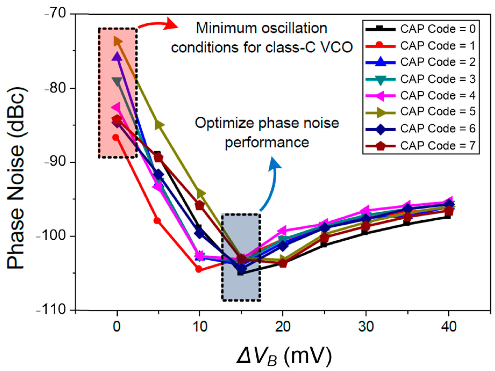
Class-C VCO requires some minimum gate bias voltage to start oscillation. However, to obtain good phase noise, a slightly higher gate bias is required than when starting oscillation. Figure 3 shows the difference in phase noise at 1-MHz offset frequency according to the additional bias voltage through the simulation and is the result of the entire code of the cap-bank. As a result, the point with the optimum phase noise performance is determined when the bias is further increased by 15 mV at the lowest oscillation condition. As the gate bias of the core transistor is increased, the oscillation amplitude also increases as the current increases. However, until the gate bias increases by 15 mV from the minimum oscillation point, the oscillation amplitude increases less steeply than the rate at which the thermal noise increases, so it becomes the lowest point with low phase noise performance [10]. Therefore, the proposed class-C VCO uses a digital to analog converter (DAC) to set the bias to the optimal point.
2.2. Proposed Auto-Adaptive Bias Controller
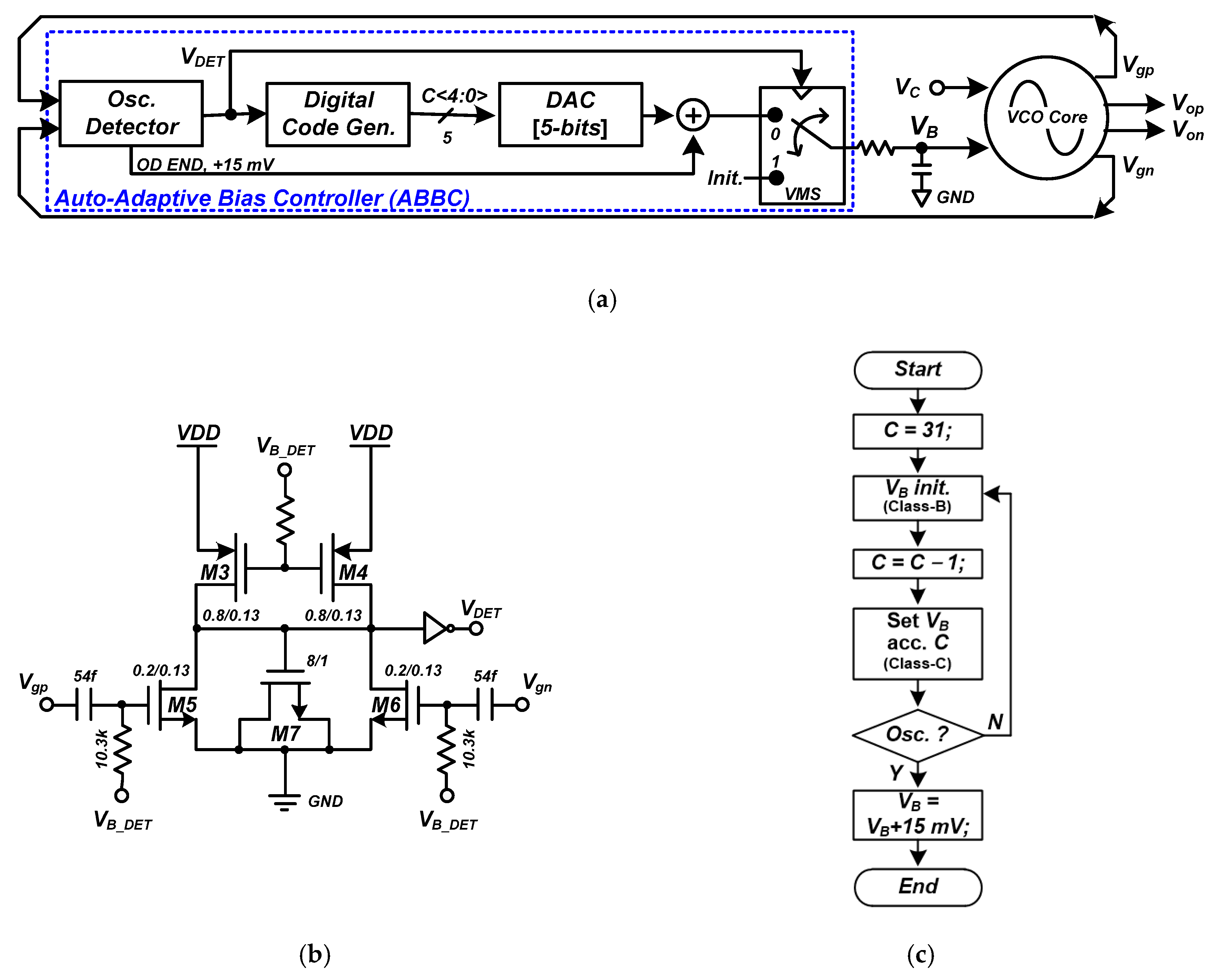
Figure 4a shows the block diagram of the proposed class-C VCO that digitally controls the auto-adaptive bias controller (AABC). The AABC prevents start-up failure and holds the gate bias point (in this figure, VB) with optimal phase noise. AABC consists of VCO mode selector (VMS), digital code generator (DCG), 5-bit DAC and oscillation detector (OD).
The VMS has two functions—class-C mode to find gate bias from DAC and class-B mode to provide VDD/2 (500 mV). The DAC outputs 405 mV at the lowest code 0 and 250 mV at the maximum code 31, 5 mV for 1 LSB. If the VCO does not oscillate sufficiently, VDET, the output of the OD, acts as a trigger to change the mode of the VMS. VMS repeats class-C and class-B modes according to VDET until VB satisfies the minimum oscillation condition. When the VCO finds a VB with sufficient oscillation conditions, it outputs an end signal from the OD and adds 15 mV verified through simulation to the VB to find the optimal phase noise point. At this time, DCG changes the code whenever the trigger signal VDET is HIGH.
Figure 4b is a schematic of OD implemented using the square-law characteristic of a MOSFET operating in the saturation region [15]. The gates of the input NMOS M5 and M6 of OD are connected to Vgp and Vgn of VCO, respectively. NMOS M7 is used as a MOS capacitor and serves to low pass filter the input signal and its harmonics. The bias between M3 and M4 and the bias connected to M5 and M6 were all applied as VB_DET, which has a value of VDD/2. The differential signal detected by the OD has a peak-to-peak voltage of 0.8-V and a target frequency of 24-GHz.
Figure 4c is a flowchart of the simple operation of ABBC. When ABBC starts operating, C code is set to 31, which is full code and VB initializes VDD/2 so that it can perform a class-B operation. After that, the class-B and class-C modes are repeatedly operated and the C code is lowered one by one and the VB value is set according to the C code value to find the oscillating point. If the oscillation continues even though the mode is changed from class-B to class-C, the VB at that time becomes the point where ΔVB is 0, that is, the minimum oscillation voltage. Then, 15 mV is added to VB according to the END signal rising edge to find the optimal phase noise point and the ABBC operation ends.
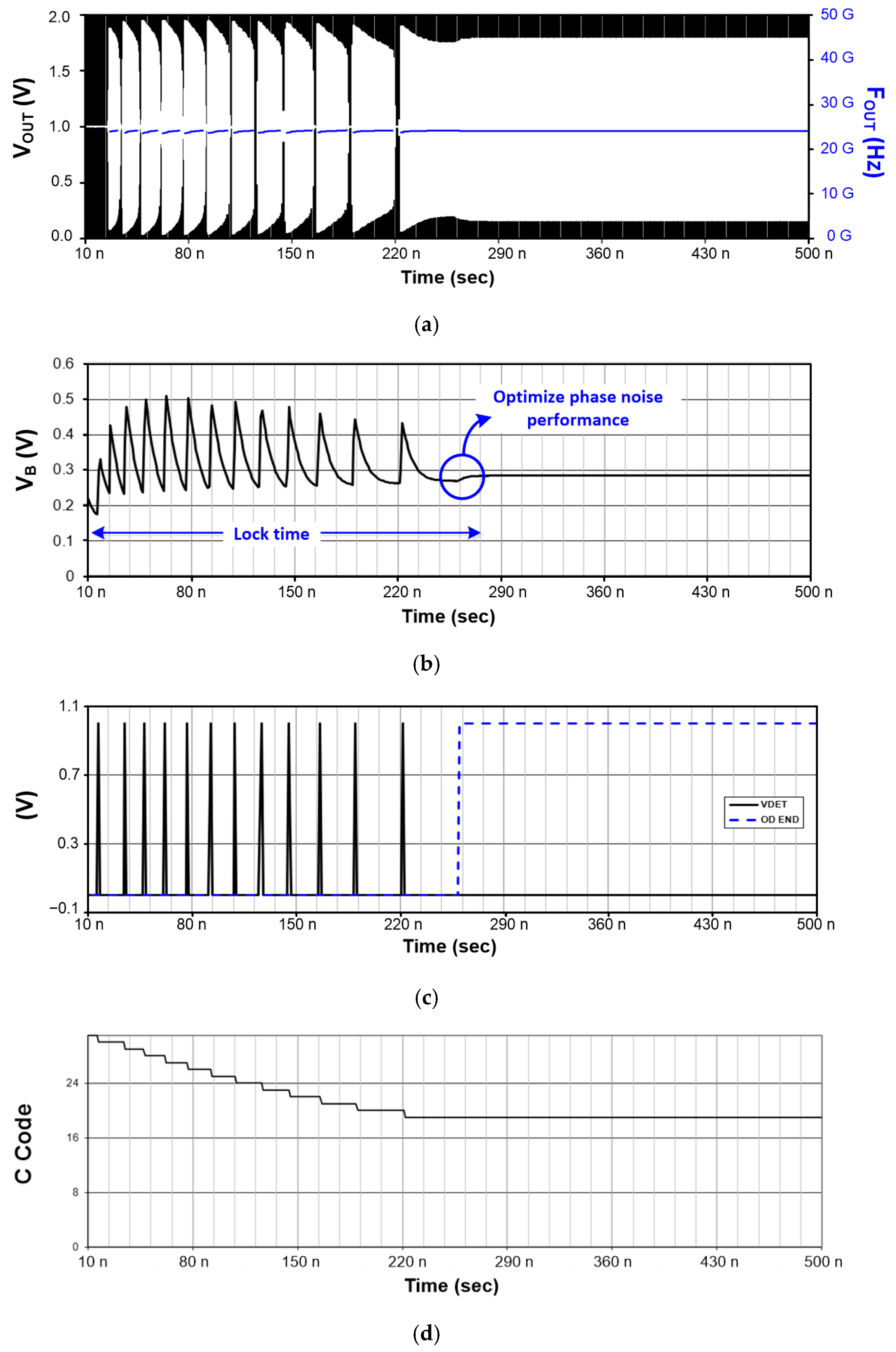
Figure 5 shows the transient simulation results of the proposed class-C VCO with AABC. This is the result of the VCO output and its frequency, the gate bias, VB, the OD output, VDET and END signal and the code of DAC output. When the first VCO starts-up, VB is brought to VDD/2 to start the oscillation.
Figure 5a shows the output voltage and frequency of the proposed class-C VCO and it is possible to check whether the VCO oscillates and the peak-to-peak voltage of the output voltage. The output frequency of the VCO does not change when AABC is operating and finding the optimal phase noise point. Figure 5b shows the change in VB voltage when the proposed class-C VCO operates. To find the lowest oscillation condition, VB repeats the voltage according to the initial values of VDD/2 and C code. In other words, make the VCO repeat class-B and class-C operations. Because the slew rate exists, VB reaches to near VDD/2. If the VCO maintains the oscillation state at any moment in the VB that changes by 1 LSB, then this is the moment when the minimum oscillation condition is satisfied. After that, OD gives an END signal and adds 15 mV to become a class-C VCO with optimal phase noise. Figure 5c shows the output signal and END signal of VDET and Figure 5d shows the C code that changes by 1 LSB for each rising edge of VDET.
The proposed AABC operates in asynchronous way without external clocked control. The time required for the VCO to find the minimum oscillation condition for class-C mode is <200 ns. The stabilization time depends on PVT variation and capacitor bank code, however, at worst case the settling time is <400 ns.
3. Measurement Results
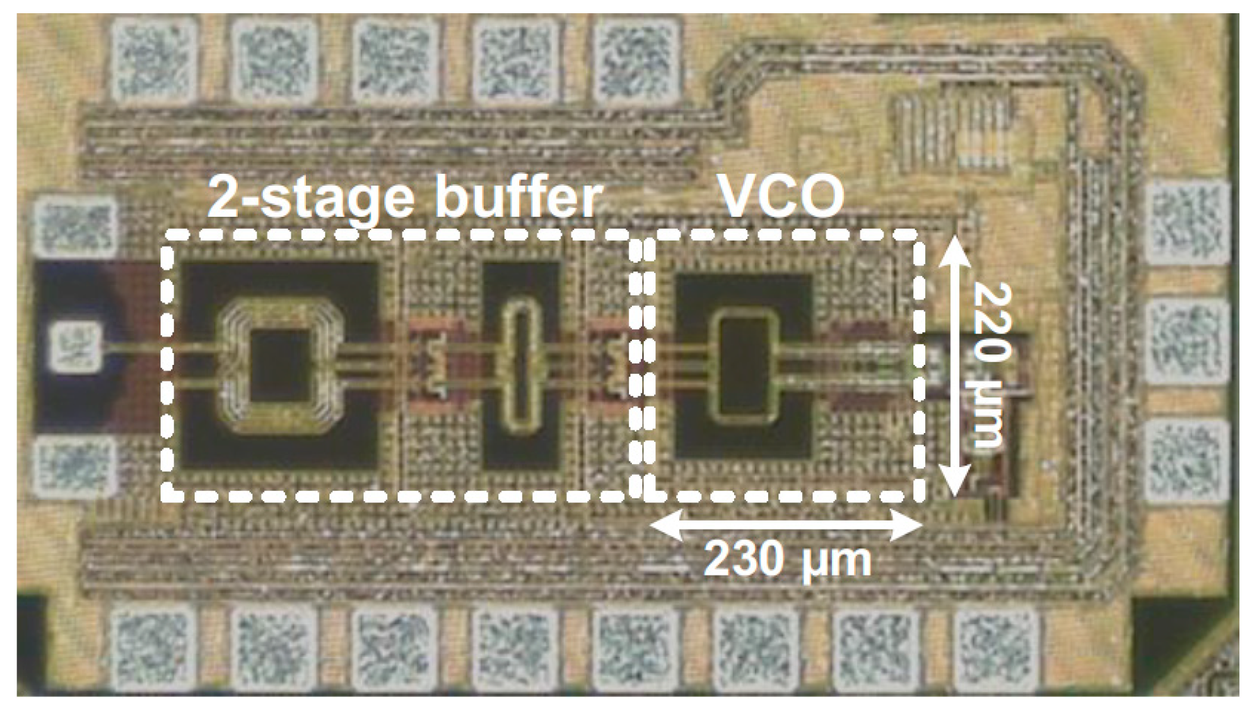
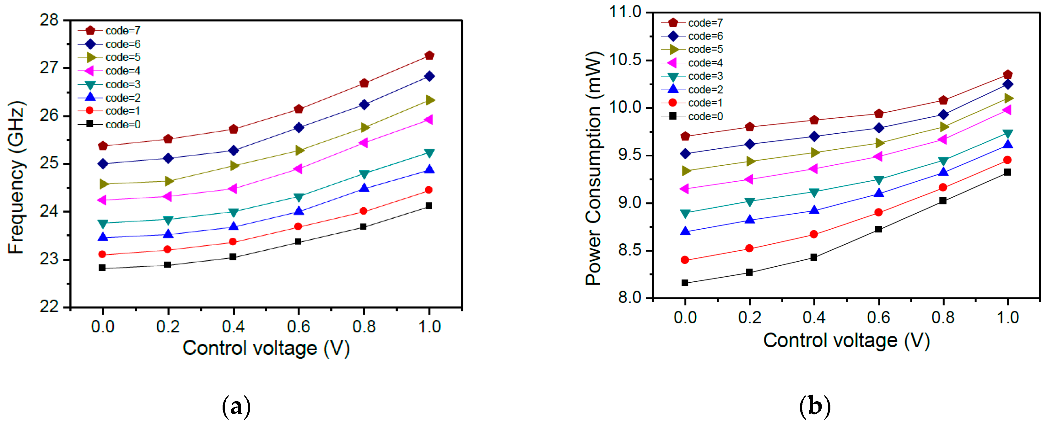
The proposed 24-GHz class-C VCO with ABBC using triple coupled transformer used a 65-nm TSMC RF CMOS process. Figure 6 shows the die photograph of the produced VCO. The core size excluding the buffer of the proposed VCO is 0.23 × 0.22 mm2. Figure 7a shows the output frequency according to the control voltage. The output frequency range is 22.8 to 27.3-GHz and the tuning range is 4.5-GHz, reaching 17.8%. Figure 7b shows the power consumption according to the control voltage. The control voltage means the voltage between varactors and both plots are the results when the cap-bank code is swept from 0 to 7.
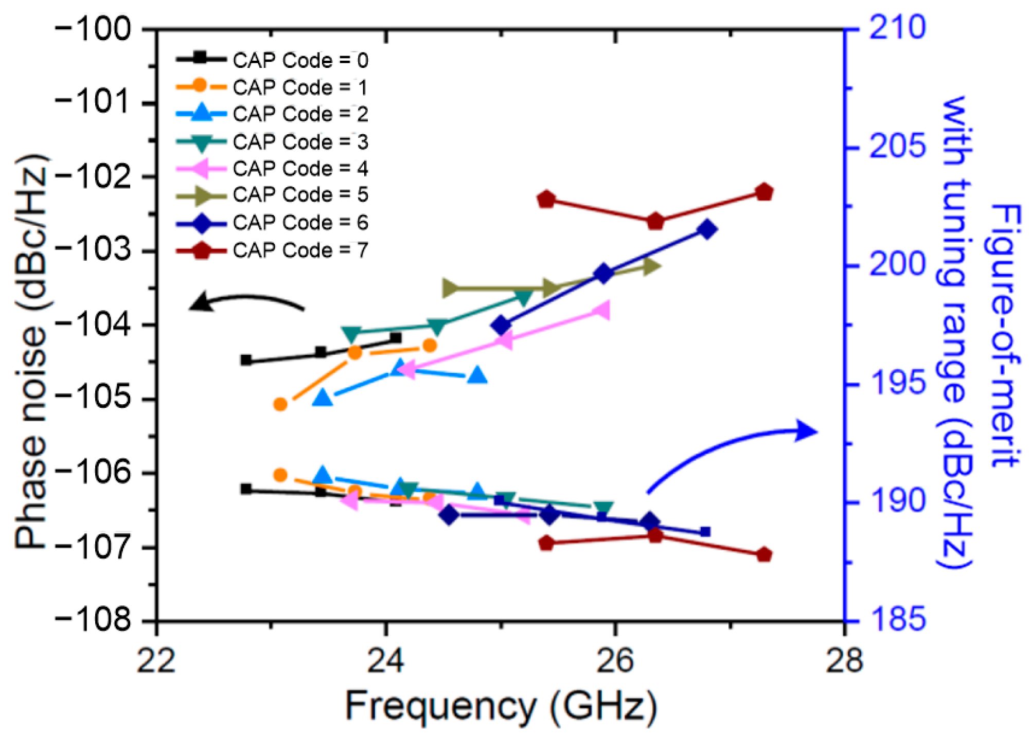
Figure 8 shows the phase noise at 24-GHz of the proposed class-C VCO and the offset frequency −105 and −128.2 dBc/Hz at 1-MHz and 10-MHz respectively at 1-V supply voltage. The phase noise that changes when the cap-bank code changes are less than 2-dB. The output frequency and phase noise can be obtained using the Agilent E4440A spectrum analyzer (Agilent Technologies, Santa Clara, CA, USA) and E5052B signal source analyzer (Keysight Technologies, Santa Rosa, CA, USA). Figure 9 shows the result of measuring the phase noise and figure-of-merit with tuning range (FoMT) at 1-MHz offset according to the frequency. FoMT according to the phase noise is −185.5 to −192 dBc. The formula of standard FoM is as follows:
and the equation for FoMT is as follows:
Here, L(Δf) is phase noise at a specific offset frequency and FTR is frequency tuning range in percent. PDC is the power consumption of VCO core and the unit is milliwatt.
The proposed class-C VCO adopts a simple but powerful auto-adaptive bias technique, as summarized in Table 2. Although phase noise is not better than other previous studies, this VCO has comparable less power consumption, wide frequency tuning range, low FoMT and smaller chip area than other class-C VCO studies [7,8,14,16,17].
4. Conclusions
In this paper, a class-C VCO using a digitally controlled auto-adaptive bias technology is proposed with a triple transformer configuration. It can have low phase acquisition, low power consumption, high frequency and a wide frequency range, simultaneously. The NMOS class-C VCO is combined using an 8-port transformer in a small chip area. The proposed VCO shows low phase noise of −105 dBc/Hz at 1-MHz offset frequency at 24-GHz with high FoMT of 191.1 dBc/Hz. The power consumption of each main block of the proposed class-C VCO is 460 μW for AABC and 8.7 mW for core, a total of 9.2 mW. The frequency tuning range is about 17.8% from 22.8 GHz to 27.3 GHz. The proposed class-C VCO implements 65-nm TSMC RF CMOS process and chip area of the core is 0.23 × 0.22 mm2.
Author Contributions
Conceptualization, J.-Y.L.; methodology, J.-Y.L.; software, J.-Y.L. and G.S.K.; validation, J.-Y.L. and G.S.K.; formal analysis, J.-Y.L.; investigation, J.G.P.; resources, K.-I.O.; data curation, G.-H.K.; writing—original draft preparation, J.-Y.L.; writing—review and editing, G.S.K.; visualization, G.S.K.; supervision, D.B.; project administration, D.B.; funding acquisition, D.B. All authors have read and agreed to the published version of the manuscript.
Funding
This work was supported by the Institute for Information & Communications Technology Planning & Evaluation (IITP) grant funded by the Korea government (MSIT) (No.2019-0-00138, Development of Intelligent Radar Platform Technology for Smart Environments) and (No.1711081183, Development of Communication-Sensing Converged B5G Millimeter Wave System) and by the Chung-Ang University Research Scholarship Grants in 2019.
Conflicts of Interest
The authors declare no conflict of interest.
References
- Long, J.R. Monolithic Transformers for Silicon RF IC Design. IEEE J. Solid-State Circuits 2000, 35, 1368–1382. [Google Scholar] [CrossRef]
- Nguyen, T.; Lee, J.-W. Ultralow-Power Ku-Band Dual-Feedback Armstrong VCO with a Wide Tuning Range. IEEE Trans. Circuits Syst. II Exp. Briefs 2012, 59, 394–398. [Google Scholar] [CrossRef]
- Hou, J.-A.; Wang, Y.-H. A 7.9 GHz Low-Power PMOS Colpitts VCO Using the Gate Inductive Feedback. IEEE Microw. Wireless Compon. Lett. 2010, 20, 223–225. [Google Scholar] [CrossRef]
- Park, J.; Park, J.; Choi, Y.; Sim, K.; Baek, D. A Fully-Differential Complementary Hartley VCO in 0.18 μm CMOS Technology. IEEE Microw. Wireless Compon. Lett. 2010, 20, 91–93. [Google Scholar] [CrossRef]
- Su, Y.-P.; Hu, W.-Y.; Lin, J.-W.; Chen, Y.-C.; Sezer, S.; Chen, S.-J. Low power Gm-boosted differential Colpitts VCO. In Proceedings of the IEEE SOC Conference (SOCC), Taipei, Taiwan, 26–28 September 2011; pp. 247–250. [Google Scholar]
- Deng, W.; Okada, K.; Matsuzawa, A. Class-C VCO with amplitude feedback loop for robust start-up and enhanced oscillation swing. IEEE J. Solid-State Circuits 2013, 48, 429–440. [Google Scholar] [CrossRef]
- Zhu, Z.; Liang, L.; Yang, Y. A Startup Robust Feedback Class-C VCO with Constant Amplitude Control in 0.18$\mu $ m CMOS. IEEE Microowave Wirel. Compon. Lett. 2015, 25, 541–543. [Google Scholar] [CrossRef]
- Amin, M.T.; Yin, J.; Mak, P.I.; Martins, R.P. A 0.07 mm2 2.2 mW 10 GHz current-reuse class-B/C hybrid VCO achieving 196-dBc/Hz FoM (A). IEEE Microw. Wireless Compon. Lett. 2015, 25, 457–459. [Google Scholar] [CrossRef]
- Song, J.-H.; Kim, B.-S.; Nam, S. An adaptively biased class-C VCO with a self-turn-off auxiliary class-B pair for fast and robust startup. IEEE Microw. Wireless Compon. Lett. 2016, 26, 34–36. [Google Scholar] [CrossRef]
- Mazzanti, A.; Andreani, P. Class-C harmonic CMOS VCOs, with a general result on phase noise. IEEE J. Solid-State Circuits 2008, 43, 2716–2729. [Google Scholar] [CrossRef]
- Chen, J.; Jonsson, F.; Carlsson, M.; Hedenas, C.; Zheng, L.R. A Low Power, Startup Ensured and Constant Amplitude Class-C VCO in 0.18 um CMOS. IEEE Microwave Wirel. Compon. Lett. 2011, 21, 427–429. [Google Scholar] [CrossRef]
- Mazzanti, A.; Andreani, P. A Push–Pull Class-C CMOS VCO. IEEE J. Solid-State Circuits 2013, 48, 724–732. [Google Scholar] [CrossRef]
- Fanori, L.; Andreani, P. Highly efficient class-C CMOS VCOs, including a comparison with class-B VCOs. IEEE J. Solid-State Circuits 2013, 48, 1730–1740. [Google Scholar] [CrossRef]
- Padovan, F.; Tiebout, M.; Mertens, K.L.R.; Bevilacqua, A.; Neviani, A. Design of low-noise K -band SiGe bipolar VCOs: Theory and implementation. IEEE Trans. Circuits Syst. I Reg. Papers 2015, 62, 607–615. [Google Scholar] [CrossRef]
- Garampazzi, M.; Mendes, P.M.; Codega, N.; Manstretta, D.; Castello, R. Analysis and design of a 195.6 dBc/Hz peak FoM PN class-B oscillator with transformer-based tail filtering. IEEE J. Solid-State Circuits 2015, 50, 1657–1668. [Google Scholar] [CrossRef]
- Franceschin, A.; Andreani, P.; Padovan, F.; Bassi, M.; Bevilacqua, A. A 19.5-GHz 28-nm Class-C CMOS VCO, With a Reasonably Rigorous Result on 1/f Noise Upconversion Caused by Short-Channel Effects. IEEE J. Solid-State Circuits 2020, 55, 1842–1853. [Google Scholar] [CrossRef]
- Mahalingam, N.; Ma, K.; Yeo, K.S.; Lim, W.M. K-band high-PAE wide-tuning-range VCO using triple-coupled LC tanks. IEEE Trans. Circuits Syst. II Exp. Briefs 2013, 60, 736–740. [Google Scholar] [CrossRef]
Figure 1.
This figure is the circuit diagram of the basic structure for differential LC voltage-controlled oscillator (VCO). (a) is a classical class-B VCO and (b) is the basic class-C VCO structure and (c) is the transformer center-tap biased class-C VCO.
Figure 1.
This figure is the circuit diagram of the basic structure for differential LC voltage-controlled oscillator (VCO). (a) is a classical class-B VCO and (b) is the basic class-C VCO structure and (c) is the transformer center-tap biased class-C VCO.

Figure 2.
This figure is the circuit diagram of the core part of the proposed class-C VCO and the figure of the transformer. (a) is the VCO of NMOS cross-coupled differential structure. It uses a varactor, a 3-bit cap-bank and three inductors. (b) is a 3-D drawing of transformers for three inductors and (c) is a simulation results plotting L and Q-factor according to the frequency change of transformers.

Figure 3.
This figure is the simulation result of phase noise at 1 MHz offset frequency for the gate bias variation (ΔVB) from the lowest oscillation voltage of the proposed class-C VCO core transistor.
Figure 3.
This figure is the simulation result of phase noise at 1 MHz offset frequency for the gate bias variation (ΔVB) from the lowest oscillation voltage of the proposed class-C VCO core transistor.

Figure 4.
This figure is (a) block diagram of proposed ABBC and class-C VCO, (b) is a circuit diagram of oscillation detector (OD).and (c) the operation is simply expressed in a flow chart.
Figure 4.
This figure is (a) block diagram of proposed ABBC and class-C VCO, (b) is a circuit diagram of oscillation detector (OD).and (c) the operation is simply expressed in a flow chart.

Figure 5.
This figure is the simulation result of the proposed class-C VCO. It is the result of output (a) voltage VOUT, output frequency FOUT, (b) gate bias VB, (c) OD output VDET and END signal and (d) 5-bit digital to analog converter (DAC) output.
Figure 5.
This figure is the simulation result of the proposed class-C VCO. It is the result of output (a) voltage VOUT, output frequency FOUT, (b) gate bias VB, (c) OD output VDET and END signal and (d) 5-bit digital to analog converter (DAC) output.

Figure 6.
This figure is a die photograph of proposed class-C VCO.

Figure 7.
This figure is a plot showing the measured results. (a) shows the output frequency according to the VCO 3-bit cap-bank control code and (b) shows the power consumption for the output frequency.
Figure 7.
This figure is a plot showing the measured results. (a) shows the output frequency according to the VCO 3-bit cap-bank control code and (b) shows the power consumption for the output frequency.

Figure 8.
This figure is a measurement of phase noise at 24-GHz output frequency.

Figure 9.
This figure shows the change of phase noise and FoMT at 1-MHz offset frequency according to cap-bank code and VCO output frequency.
Figure 9.
This figure shows the change of phase noise and FoMT at 1-MHz offset frequency according to cap-bank code and VCO output frequency.


Table 1.
This table shows the proposed VCO parameter values.
| VCO Parameters | |||
|---|---|---|---|
| Ccap-bank | 11–101 fF | Qcap-bank | 24–40 |
| L1 | 185 pH | K12 | 0.68 |
| L2 | 215 pH | K23 | 0.56 |
| L3 | 276 pH | K13 | 0.53 |
| QL1 | 20.35 | Cvar | 171 fF |
| QL2 | 7.89 | WM1 | 32 μm |
| QL3 | 3.98 | WM2 | 32 μm |
Table 2.
Performance comparison with published class-C VCO.
| This Work | [7] | [8] | [14] | [16] | [17] | Unit | |
|---|---|---|---|---|---|---|---|
| Tech. | 65 | 180 | 65 | SiGe HBT | 28 | 180 SiGe | nm |
| Config. | Class-C | Class-C | Class-B/C | Class-B/C | Class-C | - | - |
| Freq. | 22.8–27.3 | 4.74–4.85 | 10.2–11.2 | 22.7 | 19.5 | 22.5–26.2 | GHz |
| FTR | 17.8 | 2.3 | 9.6 | 13 | 12 | 15.31 | % |
| L(1-MHz) | −105 | −125 | −107.7 | −114 | −112 | −107.7 | dBc/Hz |
| FoM | −186.2 | −193 | −185 | −189 | −185 | −186.9 | dBc/Hz |
| FoMT | −191.1 | −180.6 | −185 | −193 | −186.6 | −190.6 | dBc/Hz |
| PDC | 9.2 | 3.4 | 2.2 | 18 | 20.7 | 8.2 | mW |
| Area | 0.055 | 0.15 | 0.07 | - | 0.07 | 0.28 | mm2 |
© 2020 by the authors. Licensee MDPI, Basel, Switzerland. This article is an open access article distributed under the terms and conditions of the Creative Commons Attribution (CC BY) license (http://creativecommons.org/licenses/by/4.0/).
Share and Cite
MDPI and ACS Style
Lee, J.-Y.; Kim, G.S.; Ko, G.-H.; Oh, K.-I.; Park, J.G.; Baek, D. Low Phase Noise and Wide-Range Class-C VCO Using Auto-Adaptive Bias Technique. Electronics 2020, 9, 1290. https://doi.org/10.3390/electronics9081290
AMA Style
Lee J-Y, Kim GS, Ko G-H, Oh K-I, Park JG, Baek D. Low Phase Noise and Wide-Range Class-C VCO Using Auto-Adaptive Bias Technique. Electronics. 2020; 9(8):1290. https://doi.org/10.3390/electronics9081290
Chicago/Turabian StyleLee, Jeong-Yun, Gwang Sub Kim, Goo-Han Ko, Kwang-Il Oh, Jae Gyeong Park, and Donghyun Baek. 2020. "Low Phase Noise and Wide-Range Class-C VCO Using Auto-Adaptive Bias Technique" Electronics 9, no. 8: 1290. https://doi.org/10.3390/electronics9081290
Note that from the first issue of 2016, this journal uses article numbers instead of page numbers. See further details here.