A Compact UWB Bandpass Chip Filter on a GaAs Substrate with Modified Chebyshev Structure

 , ,
, ,
Abstract
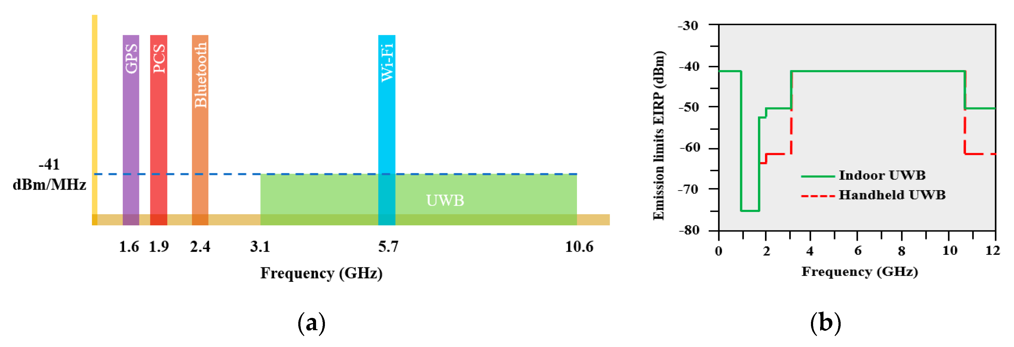
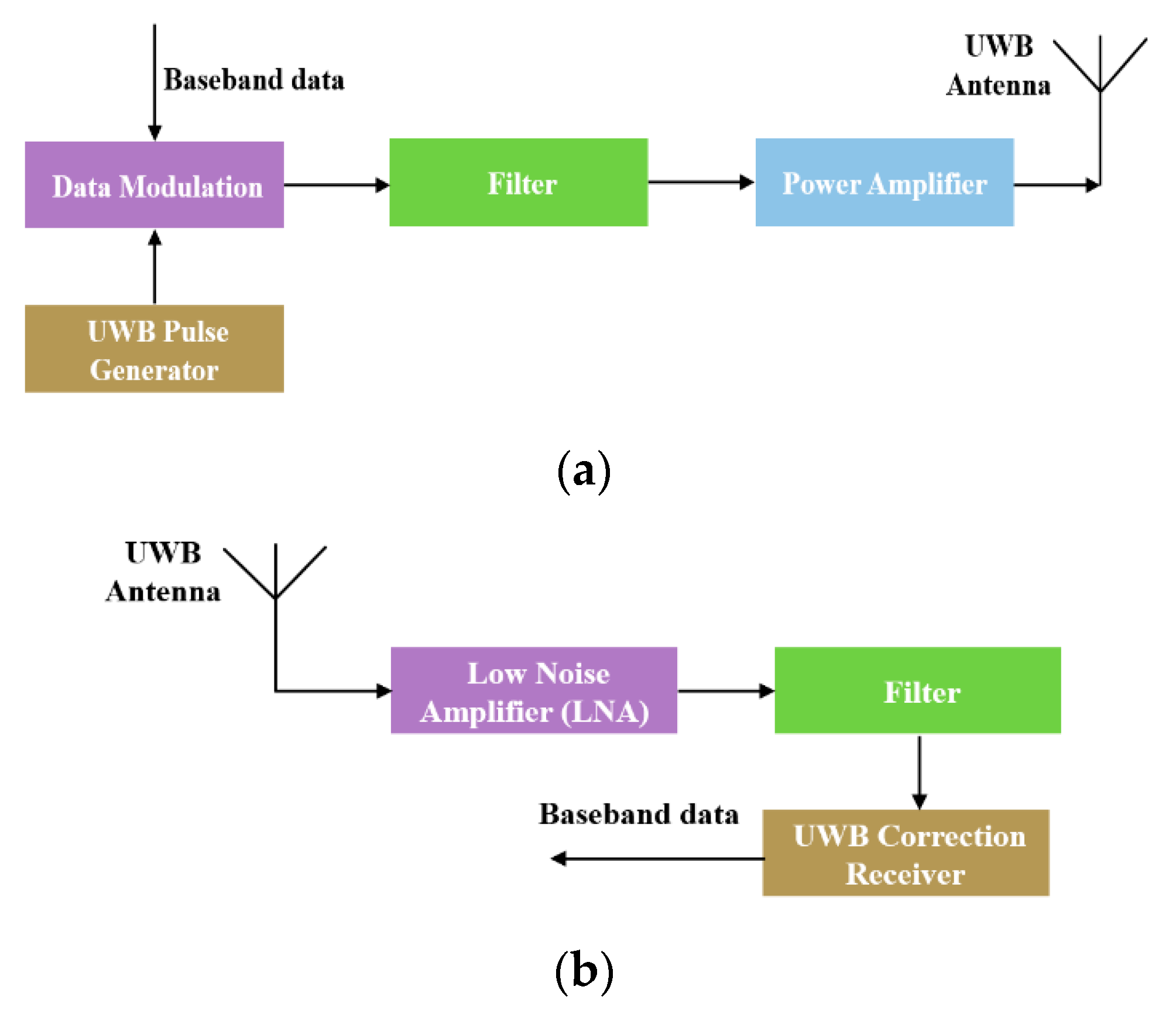
:1. Introduction
2. Materials and Methods
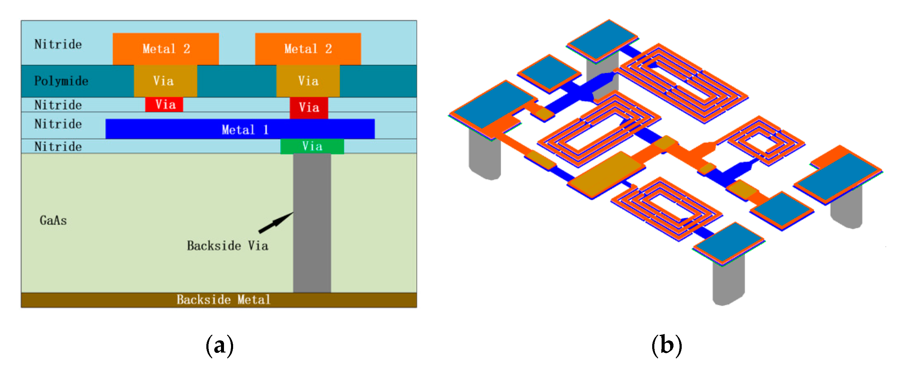
2.1. Materials and Technology
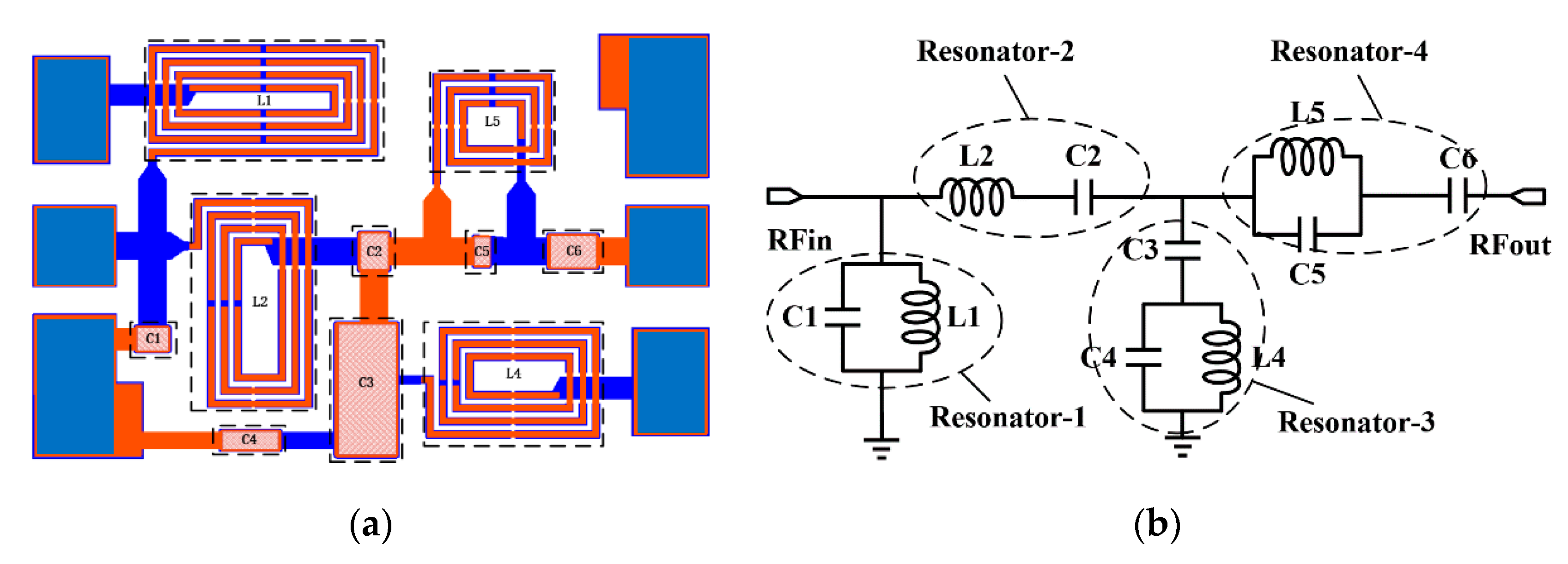
2.2. Filter Structure
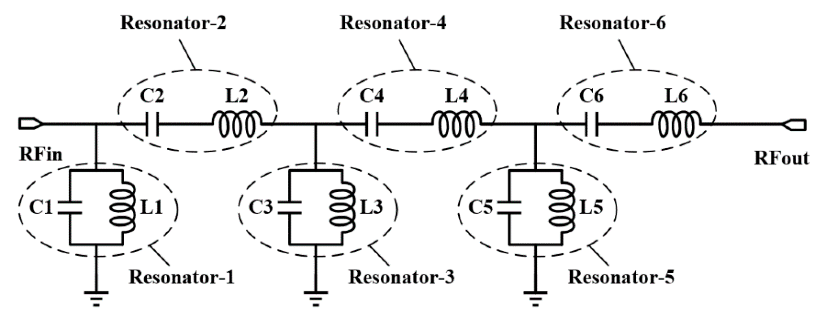
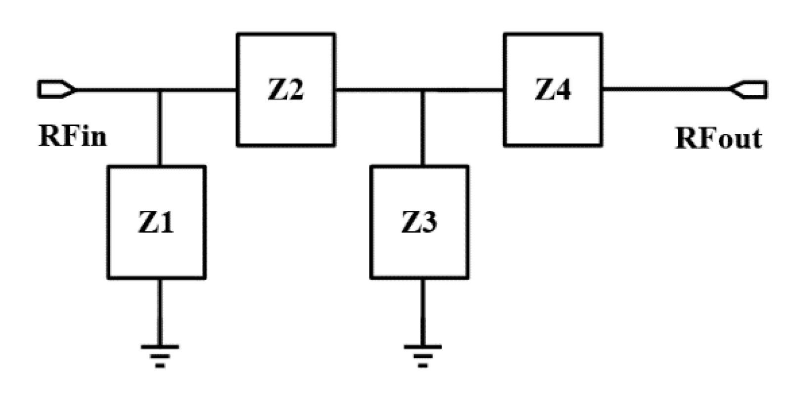
2.3. Filter Model
2.4. Filter Design and Simulation
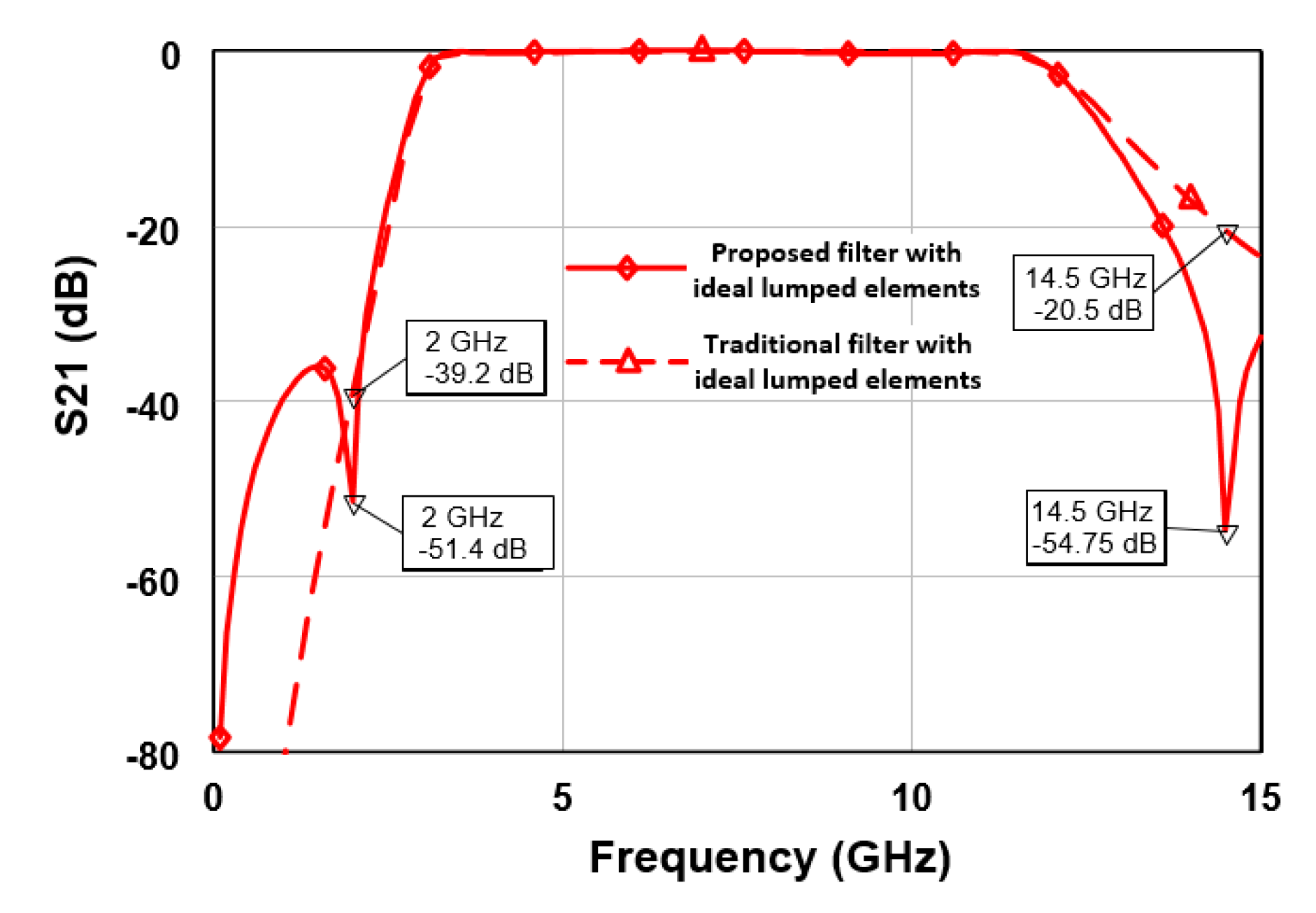
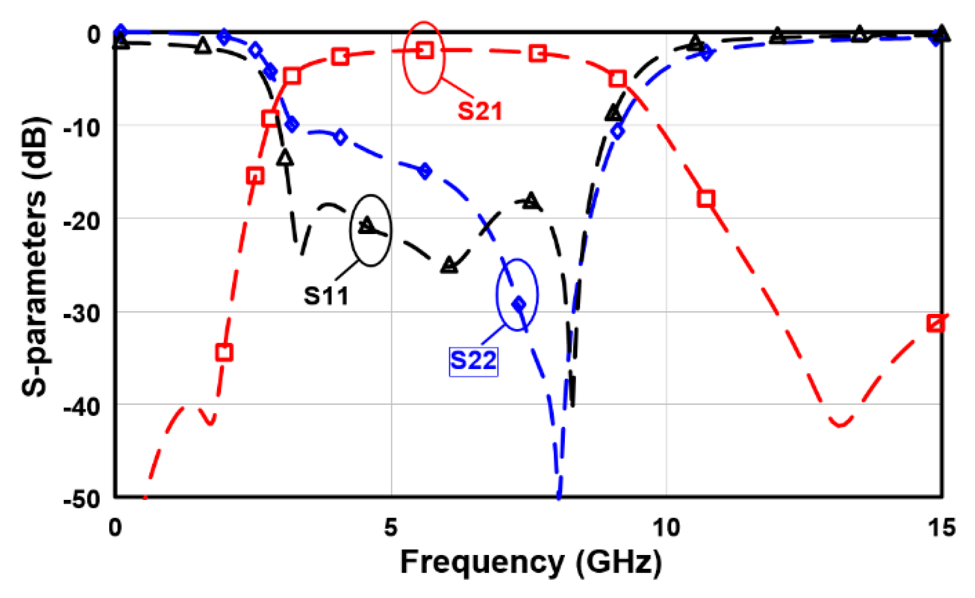
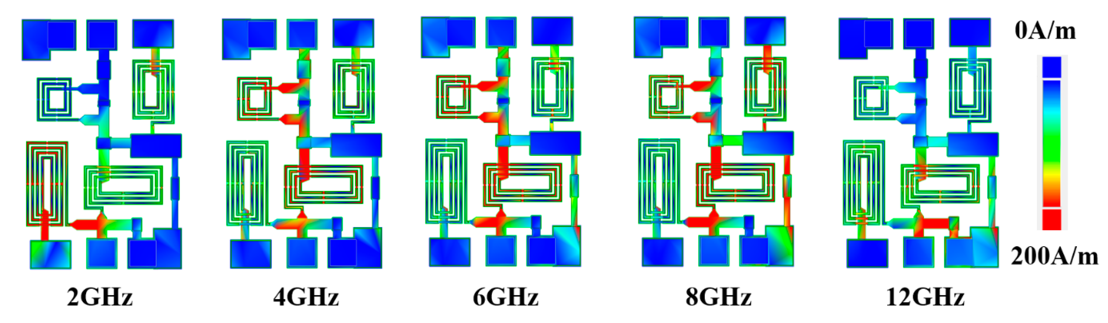
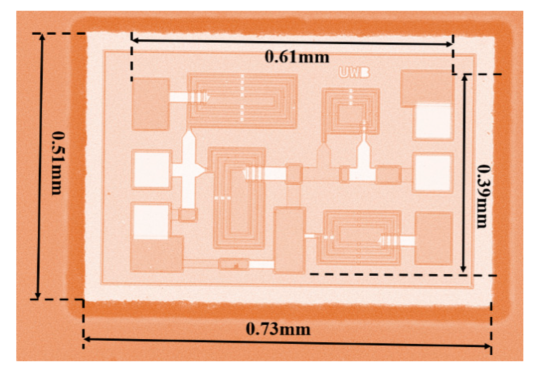
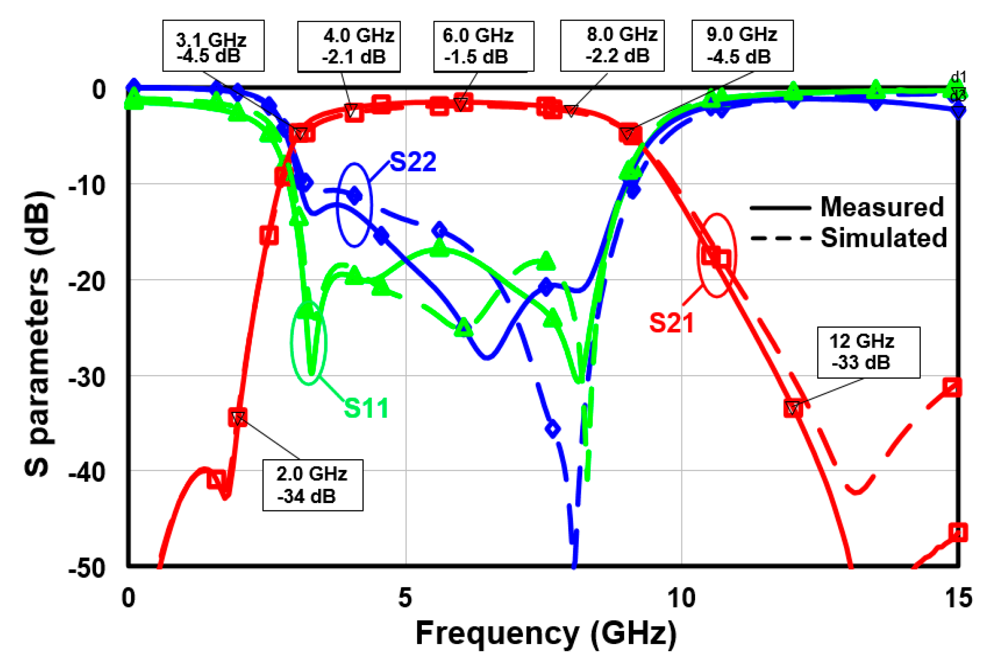
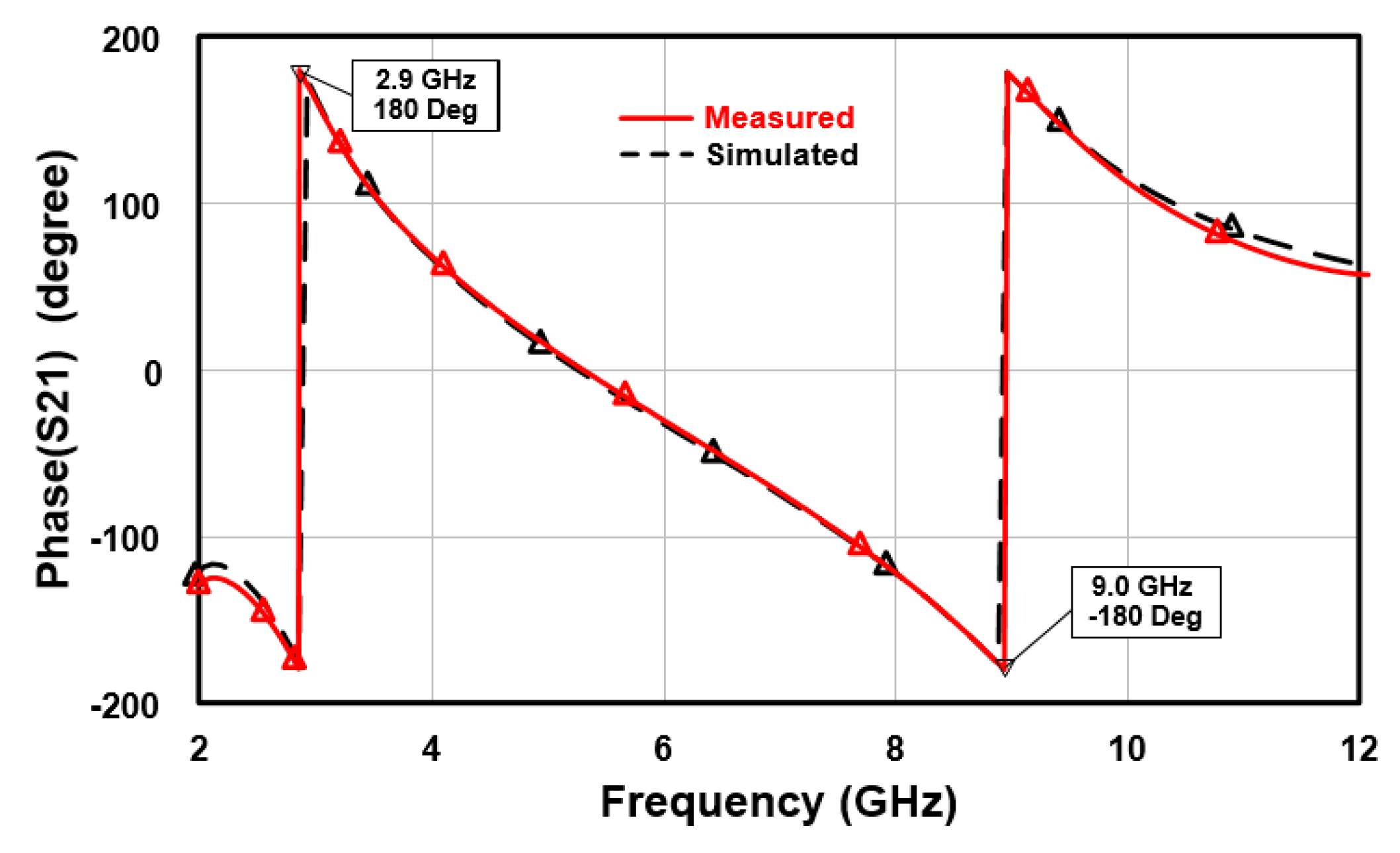
3. Results
4. Discussion
5. Conclusions
Author Contributions
Funding
Conflicts of Interest
References
- Hao, Z.C.; Hong, J.S. Ultrawideband filter technologies. Microw. Mag. IEEE 2010, 11, 56–68. [Google Scholar] [CrossRef]
- Yassin, A.; Nasser, Y.; Awad, M.; Al-Dubai, A.; Raulefs, R. Recent advances in indoor localization: A survey on theoretical approaches and applications. IEEE Commun. Surv. Tutor. 2017, 19, 1327–1346. [Google Scholar] [CrossRef] [Green Version]
- Wei, F.; Wu, Q.Y.; Shi, X.W.; Chen, L. Compact UWB bandpass filter with dual notched bands based on SCRLH resonator. IEEE Microw. Wirel. Compon. Lett. 2011, 21, 28–30. [Google Scholar] [CrossRef]
- Sekar, V.; Entesari, K. Miniaturized UWB bandpass filters with notch using slow-wave CPW multiple-mode resonators. IEEE Microw. Wirel. Compon. Lett. 2011, 21, 80–82. [Google Scholar] [CrossRef]
- Xu, J.; Wu, W.; Kang, W.; Miao, C. Compact UWB bandpass filter with a notched band using radial stub loaded resonator. IEEE Microw. Wirel. Compon. Lett. 2012, 22, 351–353. [Google Scholar] [CrossRef]
- Sarkar, P.; Ghatak, R.; Pal, M.; Poddar, D.R. Compact UWB bandpass filter with dual notch bands using open circuited stubs. IEEE Microw. Wirel. Compon. Lett. 2012, 22, 453–455. [Google Scholar] [CrossRef]
- Shen, Y.; Law, C.L. Compact UWB bandpass filter with high suppression at 2.4 and 5.8 ghz. Electron. Lett. 2012, 48, 851–853. [Google Scholar] [CrossRef]
- Wu, Z.; Shim, Y.; Rais-Zadeh, M. Miniaturized UWB filters integrated with tunable notch filters using a silicon-based integrated passive device technology. IEEE Trans. Microw. Theory Tech. 2012, 60, 518–527. [Google Scholar] [CrossRef]
- Zhang, X.Y.; Zhang, Y.W.; Xue, Q. Compact band-notched UWB filter using parallel resonators with a dielectric overlay. IEEE Microw. Wirel. Compon. Lett. 2013, 23, 252–254. [Google Scholar] [CrossRef]
- Zhu, H.; Chu, Q.X. Compact ultra-wideband (UWB) bandpass filter using dual-stub-loaded resonator (DSLR). IEEE Microw. Wirel. Compon. Lett. 2013, 23, 527–529. [Google Scholar] [CrossRef]
- Li, X.; Ji, X. Novel compact UWB bandpass filters design with cross-coupling between lambda/4 short-circuited stubs. IEEE Microw. Wirel. Compon. Lett. 2014, 24, 23–25. [Google Scholar] [CrossRef]
- Sarkar, P.; Ghatak, R.; Pal, M.; Poddar, D.R. High-selective compact UWB bandpass filter with dual notch bands. IEEE Microw. Wirel. Compon. Lett. 2014, 24, 448–450. [Google Scholar] [CrossRef]
- Kumar, S.; Gupta, R.D.; Parihar, M.S. Multiple band notched filter using c-shaped and e-shaped resonator for UWB applications. IEEE Microw. Wirel. Compon. Lett. 2016, 26, 340–342. [Google Scholar] [CrossRef]
- Kamma, A.; Das, R.; Bhatt, D.; Mukherjee, J. Multi-mode resonators based triple band notch UWB filter. IEEE Microw. Wirel. Compon. Lett. 2017, 27, 120–122. [Google Scholar] [CrossRef]
- Zhou, C.X.; Guo, P.P.; Zhou, K.; Wu, W. Design of a compact UWB filter with high selectivity and superwide stopband. IEEE Microw. Wirel. Compon. Lett. 2017, 27, 636–638. [Google Scholar] [CrossRef]
- Huang, C.C.; Fang, W.T.; Lin, Y.S. Miniaturization of broadband stub bandpass filter using bridged-t coils. IEEE Access 2018, 6, 20164–20173. [Google Scholar] [CrossRef]
- Xinlin, X.; Xu, C.; Fengjun, C.; Xianjin, D. Compact UWB bandpass filter with sharp roll-off using APCL structure. Electron. Lett. 2018, 54, 837–839. [Google Scholar]
- Xuemei, Z.; Yuwen, P.; Tao, J. UWB bandpass filter with dual notched bands using t-shaped resonator and l-shaped defected microstrip structure. Micromachines 2018, 9, 280–291. [Google Scholar]
- Lei, H.; Naichang, Y. A Compact Wideband SIW Bandpass Filter with Wide Stopband and High Selectivity. Electronics 2019, 8, 440. [Google Scholar]
- Badiaa, A.A.; Hicham, K.; Otman, A.; Ana, V.A. Selectivity and Rejection Bandwidth Improvements of a Multi-Band Stopband Filter Based on Circular Split Ring Resonator. In Proceedings of the 13th European Conference on Antennas and Propagation, Małopolskie, Poland, 1–5 April 2019. [Google Scholar]
- Cao, H.; Ying, W.; Li, H.; Yang, S. Compact lowpass filter with wide stopband using novel windmill resonator. J. Electromagn. Waves Appl. 2012, 26, 2234–2241. [Google Scholar] [CrossRef]
- Naghshvarian, J.M.; Tayarani, M. Defected ground structure band-stop filter by semicomplementary split ring resonators. IET Microw. Antennas Propag. 2011, 5, 1386–1391. [Google Scholar] [CrossRef] [Green Version]
- Liu, K.; Frye, R.C.; Emigh, R. Miniaturized ultra-wideband band-pass-filter from silicon integrated passive device technology. In Proceedings of the IEEE International Microwave Symposium Digest, Boston, MA, USA, 7–12 June 2009. [Google Scholar]
- Lu, M.C.; Chang, J.F.; Lin, Y.S.; Lu, L.C. 1.89 dB insertion-loss UWB bp-filter with three finite transmission zeros using standard 0.18 μm CMOS technology. Electron. Lett. 2009, 45, 56–57. [Google Scholar] [CrossRef]
- Dine, W.G.E.; Ezzeddine, H.; Bila, S.; Verdeyme, S. Three approaches for the realization of a Chebyshev cross-coupled UWB filter. In Proceedings of the IEEE Microwave Symposium Digest, Anaheim, CA, USA, 23–28 May 2010. [Google Scholar]
- Manchec, A.; Laporte, C.; Cédric, Q.; Ezzeddine, H.; Clavet, Y.; Rius, E. Hybrid lumped/distributed band-pass filter in IPD technology for ultra-wideband applications. In Proceedings of the IEEE Microwave Symposium Digest, Baltimore, MD, USA, 5–10 June 2011. [Google Scholar]
- Tseng, T.H.; Fang, W.T.; Lin, Y.S. Super compact and ultra-wideband bandpass filter using bridged-T coils. In Proceedings of the IEEE Microwave Symposium Digest, San Francisco, CA, USA, 22–27 May 2016. [Google Scholar]


| Lumped Elements | Value | Lumped Elements | Value |
|---|---|---|---|
| L1 | 2.38 nH | C1 | 0.29 pF |
| L2 | 1.58 nH | C2 | 0.45 pF |
| L3 | 1.10 nH | C3 | 0.63 pF |
| L4 | 1.75 nH | C4 | 0.40 pF |
| L5 | 1.24 nH | C5 | 0.56 pF |
| L6 | 0.81 nH | C6 | 0.86 pF |
| Lumped Elements | Value | Lumped Elements | Value |
|---|---|---|---|
| L1 | 2.20 nH | C1 | 0.35 pF |
| L2 | 1.60 nH | C2 | 0.49 pF |
| L4 | 1.50 nH | C3 | 3.87 pF |
| L5 | 0.60 nH | C4 | 0.48 pF |
| C5 | 0.20 pF | ||
| C6 | 0.72 pF |
| Ref. | Passband (GHz) | Insertion Loss (dB) | Return Loss (dB) | Chip Size (mm × mm) | Technology |
|---|---|---|---|---|---|
| [23] | 7.0–9.0 | 2.5 | −12 | 1.6 × 1.2 | Silicon IPD |
| [24] | 3.9–9.4 | 1.89 | −11 | 0.54 × 0.497 | Silicon CMOS |
| [25] | 3.1–4.8 | 2.5 | −8 | 3.8 | Glass IPD |
| [26] | 3.1–4.8 | 2.4 | −12 | 5.0 | Glass IPD |
| [27] | 3.1–10.6 | 1.0 | −15 | 0.88 × 0.88 | GaAs pHEMT |
| This work | 3.1–9.0 | 1.5 | −11 | 0.61 × 0.39 | GaAs pHEMT |
© 2020 by the authors. Licensee MDPI, Basel, Switzerland. This article is an open access article distributed under the terms and conditions of the Creative Commons Attribution (CC BY) license (http://creativecommons.org/licenses/by/4.0/).
Share and Cite
Hu, S.; Hu, Y.; Gao, Y.; Zhang, X.; Zhang, X.; Wang, Z.; Zhou, B.; Cai, Z.; Guo, Y. A Compact UWB Bandpass Chip Filter on a GaAs Substrate with Modified Chebyshev Structure. Electronics 2020, 9, 313. https://doi.org/10.3390/electronics9020313
Hu S, Hu Y, Gao Y, Zhang X, Zhang X, Wang Z, Zhou B, Cai Z, Guo Y. A Compact UWB Bandpass Chip Filter on a GaAs Substrate with Modified Chebyshev Structure. Electronics. 2020; 9(2):313. https://doi.org/10.3390/electronics9020313
Chicago/Turabian StyleHu, Shanwen, Yunqing Hu, Yiting Gao, Xiaodong Zhang, Xinlei Zhang, Zixuan Wang, Bo Zhou, Zhikuang Cai, and Yufeng Guo. 2020. "A Compact UWB Bandpass Chip Filter on a GaAs Substrate with Modified Chebyshev Structure" Electronics 9, no. 2: 313. https://doi.org/10.3390/electronics9020313