System Level Optimization for High-Speed SerDes: Background and the Road Towards Machine Learning Assisted Design Frameworks


1812 Seville Way, San Jose, CA 95131, USA
*
Author to whom correspondence should be addressed.
Electronics 2019, 8(11), 1233; https://doi.org/10.3390/electronics8111233
Submission received: 30 September 2019
/
Revised: 21 October 2019
/
Accepted: 24 October 2019
/
Published: 28 October 2019
(This article belongs to the Special Issue Nanoscale CMOS Technologies)
Abstract
:This decade has witnessed wide use of data-driven systems, from multimedia to scientific computing, and in each case quality data movement infrastructure is required, many with SerDes as a cornerstone. On the one hand, HPC and machine learning cloud infrastructure carry exabytes of data in a year through the backplanes of data centers. On the other hand, the growing need for edge computing in the IoT places a tight envelope on the energy per bits. In this survey, we give a system level overview of the common design challenges in implementing SerDes solutions under different scenarios and propose simulation methods benefiting from advanced machine learning techniques. Preliminary results with the proposed simulation platform are demonstrated and analyzed through machine learning based design methodologies.
1. Introduction
SerDes system design concerns transferring data through high bandwidth media, such as wireline or optical channels, at very high data rates. Such systems serve as the backbone in many modern day applications, from multimedia [1], data center and cloud, and machine learning accelerations [2], to cutting edge memory systems [3], and mobile/IoT devices [4].
As the rise of data driven applications in this decade continues to call for high quality SerDes products, the use cases also diversify across different data rates, as in Figure 1, and power budgets.
One example application is data center applications [5] that demand very high bandwidth through long and lossy channels, accommodating the ever growing traffic throughout the computing clusters. Another example is memory bus systems such as [6,7], that serve as data channels in very dense parallel buses, where the design cost, power, and absolute delay are more prioritized.
The different aspects of SerDes quality translate to a wide range of design trade-offs from the system level to circuit implementations. The overall system needs to be carefully architected, balancing the power and silicon budget, the channel quality, and the performance target.
In this paper we briefly overview the major challenges that SerDes systems need to address and discuss commonly used solutions, and then a python-based system modeling package, PySerDes, is proposed to address the need for system level simulation and validation for various aspects of SerDes design, and integration of the constantly advancing optimization techniques available in the scientific community.
1.1. System Background
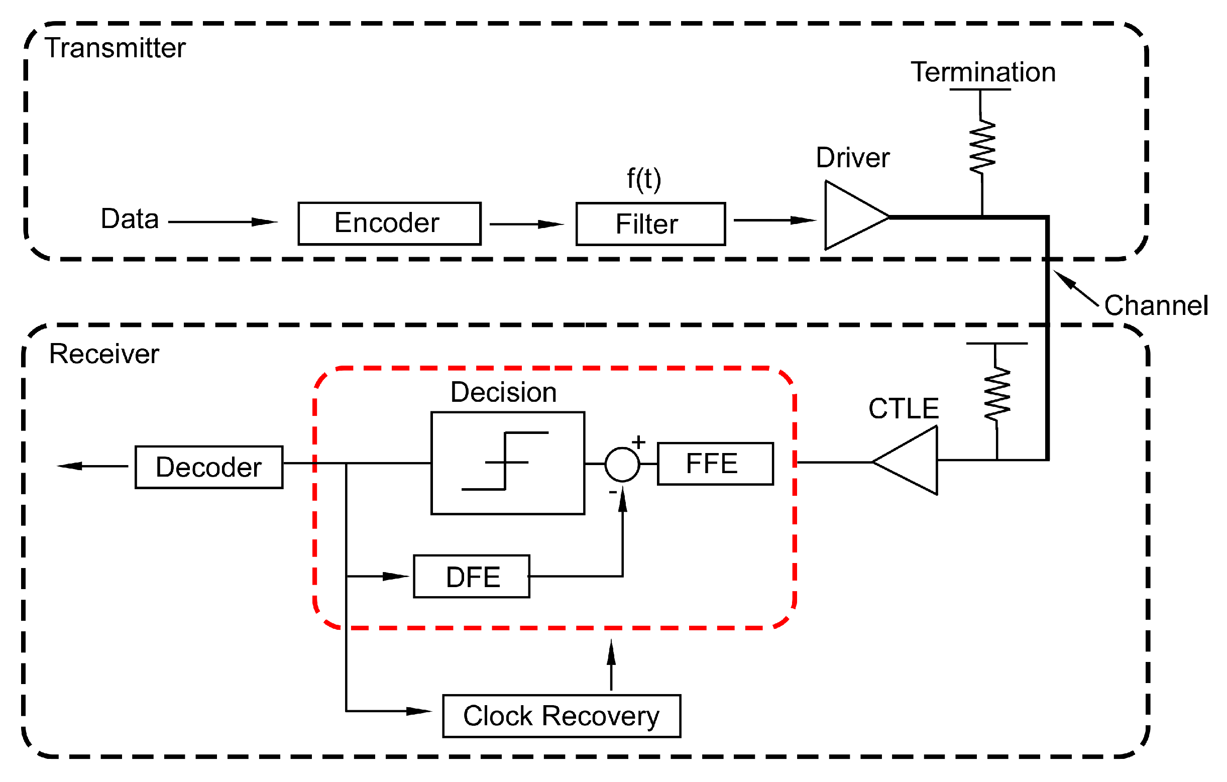
A typical single lane SerDes top level model is shown in Figure 2, that consists of a transmitter (TX) that modulates a signal with incoming bits, a channel representing the transmission media, such as a cable, and a receiver (RX) that recovers data from channel corrupted waveforms [8].
One immediate task that a SerDes system needs to address is limited bandwidth of the channel, which distorts the TX output modulated by the high speed data stream. An eye diagram is commonly used to characterize such distortion and estimate the receiver data quality. Equalization [9] is the most common technique used to address this distortion, which will be discussed in the next subsection.
Another common challenge in high speed SerDes is clock recovery [10]. As the data stream into the TX is timed through a certain clock signal, the RX needs to obtain this clock signal in order to obtain the correct bits. Typical solutions include clock forwarding, which sends the clock signal through a dedicated channel, or embedded clocking, that requires RX deriving the clock from the data channel.
Circuit non-ideality also adds to the challenges in advanced SerDes designs, due to non-ideal scaling of CMOS technologies [11], increasing performance demand and shrinking the system footprint. In the rest of this section we focus on two major topics in SerDes system design, equalization and timing recovery, along with a discussion on the effect of circuit non-ideality on the system level.
1.2. Equalization
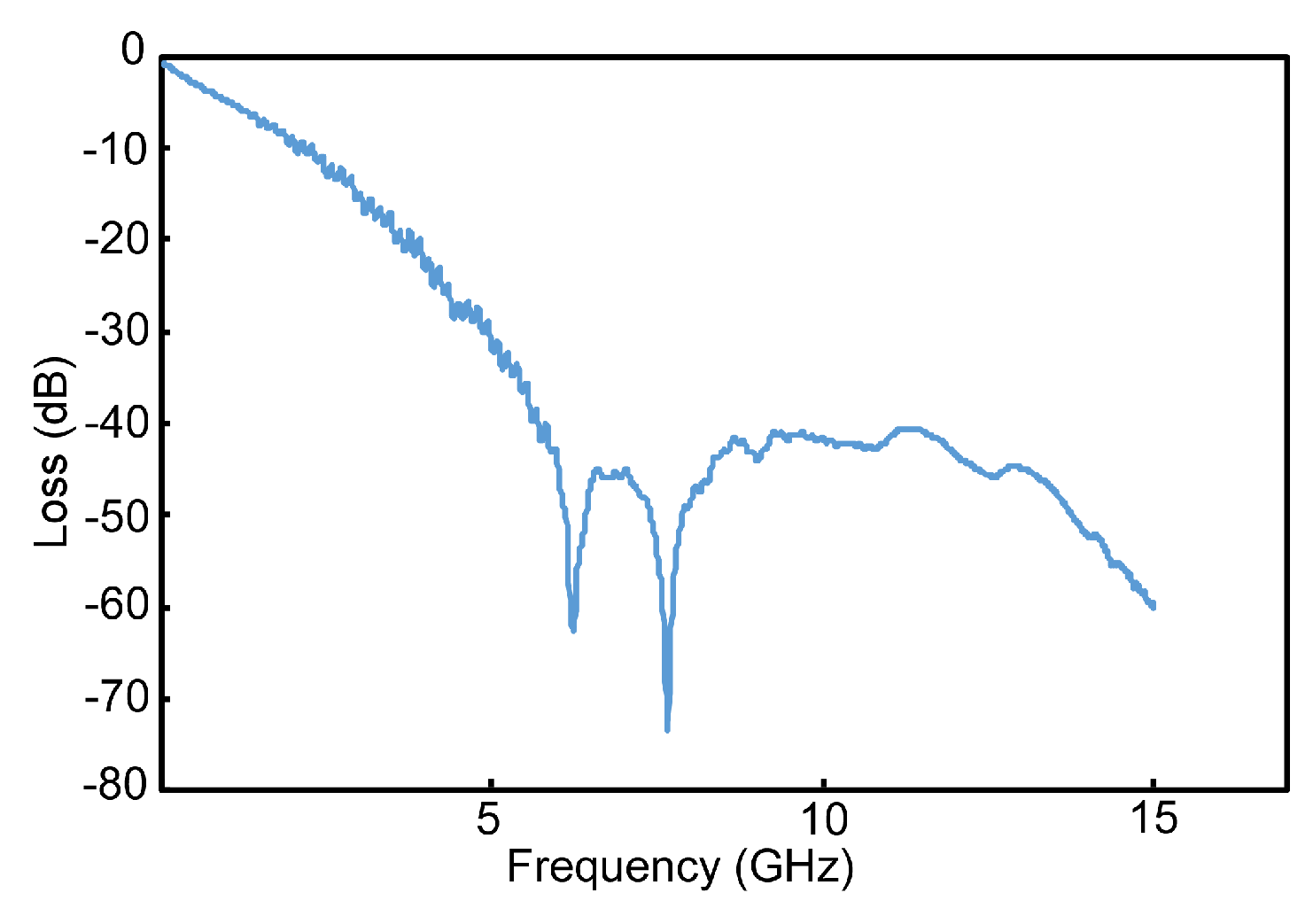
SerDes systems beyond the multi-Gbps range are often bandwidth limited, intuitively due to the fact that most physical media with the size measured beyond millimeters cannot switch at multi-GHz. Figure 3, shows a typical channel response involved in the server backplane applications [12].
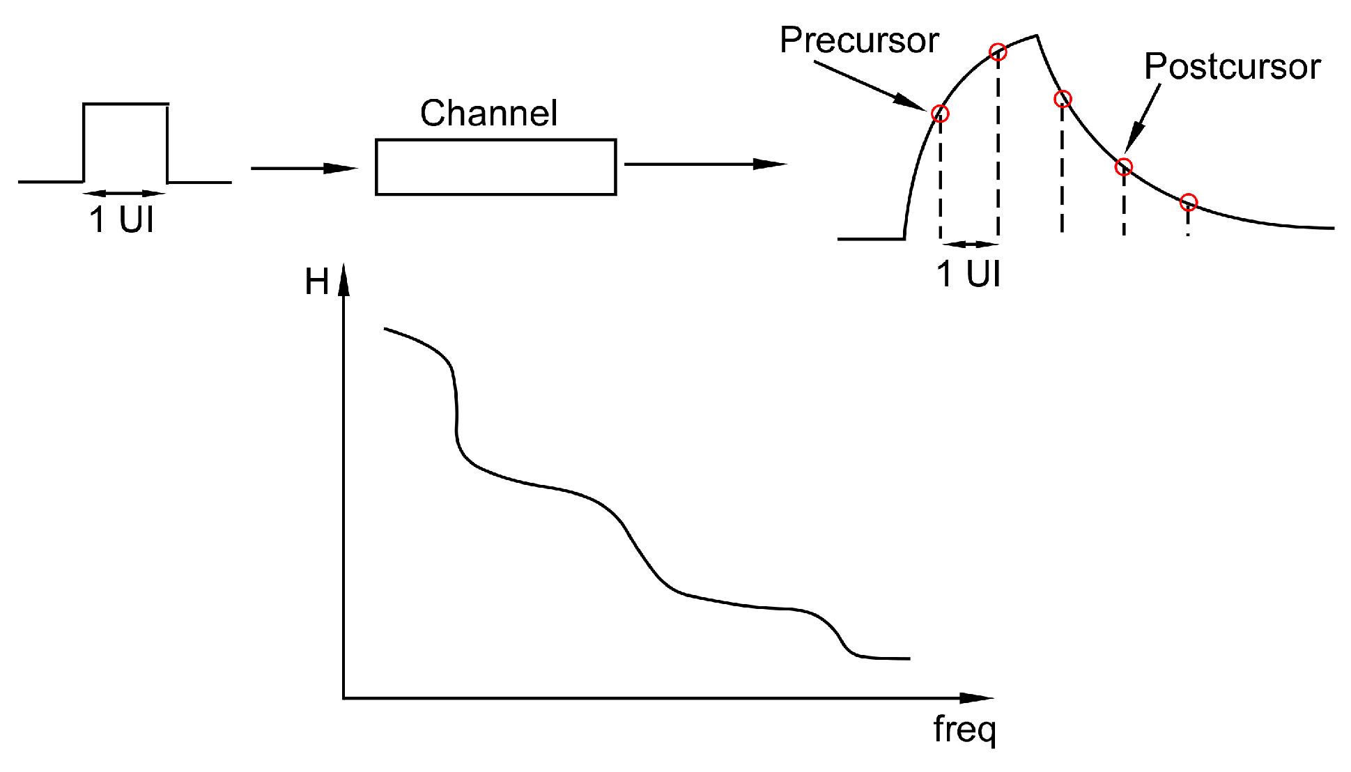
The band-limited channel response translates to inter-symbol interference (ISI) in the time domain. ISIs are usually characterized as pre-cursor and post-cursor taps after the receiver signal is sampled in discrete time. The naming can be understood as in Figure 4.
Assuming a PAM2 modulated TX and a band-limited channel, the output waveform looks like a train of square pulses, each of the length of a unit interval (UI). As we test the channel with a pulse of length 1 UI on the receiver side, the channel will be dispersed in time due to the bandwidth limitation. When it takes the pulse more than 1 UI to reach the peak, a pre-cursor ISI is produced, and when the pulse spends more than 1 UI to settle back to initial value, it causes post-cursor ISI. Typically post-cursor ISIs last much longer than pre-cursor ones due to the causality of modulation and inherent phase distortion [13].
1.2.1. System Formulation
The waveform seen at the RX side can be described by Equation (1)
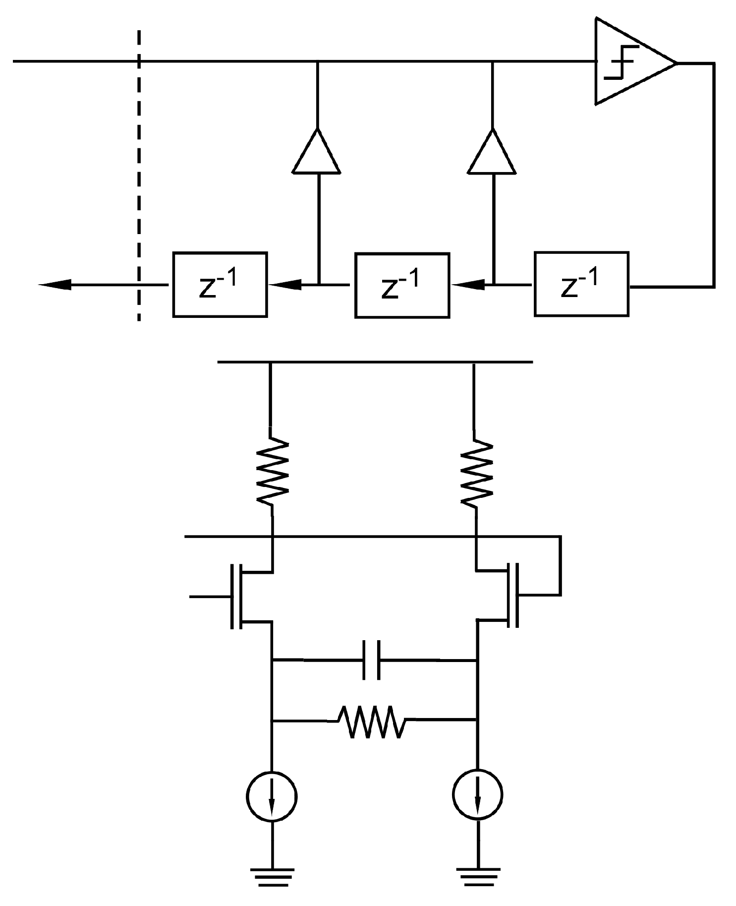
where ∗ is continous time convolution, is the impulse function, is the channel impulse response, represents transmitter side filtering, also called pre-emphasis, and represents receiver side filtering, usually implemented with a continuous time linear equalizer (CTLE) Figure 5 and finally, a feed forward equalizer (FFE). When a decision-feedback equalizer (DFE) is used, the waveform is modified as in Equation (2), where is the decision at receiver end.
Equalizer designs suppress ISI at the cost of signal-to-noise ratio, so equalization performance is usually characterized by the SNR of the equalized waveform. Under linearity assumptions on the channel characteristics, given a channel frequency response and noise power spectrum density , the optimal SNR can be characterized by the matched-filter bound (MFB) [13], which can be calculated by integrating the ratio of signal power spectrum and noise power spectrum over the band of interest.
In practice, the performance of an equalization system can be seen using an eye diagram [8]. The SNR discussed in equalization theory corresponds to the “eye-opening” at the “center”, where an optimal sample can be obtained for decoding. An eye diagram also characterizes timing jitters of the transmitter and the sampling margins on the receiver end.
The choice of equalization structure depends largely on the applications, on the low power, low loss regime, a single CTLE or even a one-tap DFE embedded in a decision circuit can be used [14]. On the high performance end is the theoretically optimal SNR under white noise achieved by the Viterbi equalizer (VE) [15]. However, the power and circuit cost in implementing an VE makes it more often seen in large scale applications [16].
1.2.2. Implementation Challenges
Silicon implementation of equalizers mostly becomes very challenging as the technology nodes continue to scale. Some notable difficulties in implementing CTLEs, essentially as a continuous time high pass filter, are the device matching, limited device bandwidth, and device noise [17]. The best known bottleneck in high speed DFE design is closing the feedback timing loop, which can be slightly mitigated by loop unrolling [9] at the cost of much more capacitance at the DFE summing node.
Additionally, circuit non-ideality contributes to many aspects of the design, making the real system deviate from Equation (2). For example, the sampling speed of the decision comparators put extra bandwidth limitations on the receiver performance, characterized by impulse sensitivity functions (ISF) [18]. The bandwidth requirement can be taken into account at the system level to explore opportunities to boost performance while saving comparator power. Another example is that non-ideal settling of the DFE feedback circuit can distort the waveform present at the decision circuit, needing extra modeling effort when the exact eye contour at the receiver end is important. A final example is when ADC is used for RX at very high loss end applications, the SNDR, bandwidth and other implementation dependent characteristics could require special effort on the system design side.
1.3. Clocking
Timing synchronization is another important task for a SerDes system. Typically the TX and RX would not share the clock source and therefore efforts need to be made for RX and TX to synchronize on both frequency and phase. Based on the phase and frequency relationships between TX and RX, the clock delivery scheme can be categorized [8] as synchronous, where TX and RX frequency and phase aligned; mesochronous, or forward clocking, where a shared frequency source is available at both TX and RX but they are not necessarily phase aligned; plesiochronous, or embedded clocking, where hints of the clock phase and frequency are contained in the TX waveform and the RX derives the clock signal from the data channel through the use of a clock data recovery (CDR) subsystem.
Trade-offs exist when selecting the clock architectures. Synchronous clocking can be used in low speed and low cost regimes, while mesochronous and plesiochornous are often implemented for high speed SerDes systems. Forward clocking costs less circuitry on the TX and RX side and usually offers more reliable synchronization performance but the cost of the extra clock channel also adds significantly to the design budget. Embedded clocking does not require the extra clock channel but both the TX and RX side become more complex to implement [19].
Key performance metrics of the clocking system include the jitter generation, jitter propagation along with the common metrics for phase lock loops (PLLs) and clock networks [19]. Typically a jitter mask is defined in industry standards to describe the requirement of SerDes clock performance [20].
Complex phase-locked loops are becoming increasingly important in SerDes systems as many of the state-of-the-art SerDes products are multi-standard.
1.4. SerDes Circuit Opportunities and Challenges
CMOS SerDes systems are typical mixed signal design applications. Scaling of CMOS technology nodes introduces challenges in many of the system building blocks, while also opening up circuit design opportunities.
On the transmitter side, the growing popularity of PAM4 modulation [5] has posed challenges on the linearity of TX drivers [21]. On the receiver side, the device scaling makes the design of quality CTLE as challenging as the design of most amplifiers. The lowered Supply Voltage and degraded transistor matching in advanced CMOS technologies also pose challenges in the design of DFE and decision circuits.
The clocking circuit design also involves difficult trade-offs. On the clock generation side, analog PLLs scale poorly with technology, all digital PLLs (ADPLLs) are sometimes considered, which introduces many other challenges from modeling to design [22]. On the clock distribution side, the increasing complexity of TX and RX designs also place higher demand on the quality of clock buffers, such as supply rejection (SR), duty cycle distortion (DCD) and rise time (RT). High performance clock distribution networks are not only challenging to build, but also often occupy much of the overall system power consumption [19]. Therefore, careful system level design and budgeting is paramount in avoiding sub-optimal operating points or over designs.
1.5. Further System Level Challenges
Further challenges exists in addition to the design of equalization and clocking systems, such as simultaneous switching noise (SSN) [23] and crosstalk [24]. Another important aspect of SerDes design is forward error correction and line coding [13]. Most of the issues need to be addressed early on in the design phase through behaviorial models of the real system.
2. PySerDes: A Behavioral Modeling Toolbox
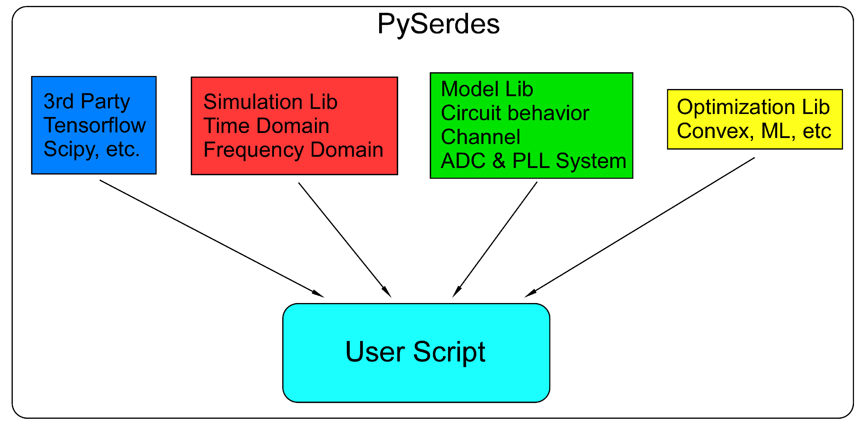
Architectural level modeling and exploration has been very common in SerDes designs, in both academic [25] and industry settings [26]. Behavioral simulation models serve many purposes throughout each phase of SerDes design, from early planning and budgeting, to quick design explorations, and also in providing references in post silicon characterization. In this work, we introduce PySerDes, an open platform for quickly prototyping SerDes systems and exploring trade-offs. PySerDes provides a series of container libraries (Figure 6) that can be flexibly integrated into the open source scientific computing eco-system and potentially supporting many SerDes system modeling experiments and analyses.
As open platforms have benefited many other research areas , such as TensorFlow [27] for machine learning research, and GEM5 [28] or FireSim [29] for computer architecture, the authors believed that a common open framework would positively influence the SerDes design community in many ways.
First, as discussed in the previous sections, many challenges across different SerDes applications, from PCIE to backplane, are actually shared, and therefore an open platform provides the means for sharing design ideas across the designer community. Secondly, cutting-edge SerDes designs are usually implemented with protected circuit blocks, and thus it is a standard practice in modeling to introduce an extra layer of abstraction, such as IBIS-AMI model for TX-CHANNLE-RX style modeling [30]. The authors believed that such standard models can be further explored through open platforms, with designers proposing abstract models through the API, and established platform infrastructure can be used to communicate, verify, and optimize the designs. Lastly, scientific open source community has grown significantly over the recent years, and the proposed PySerDes can serve as a bridge towards utilizing latest advances in relevant areas such as scientific computing, optimization, and machine learning, just to name a few.
The rest of this section introduces the modeling techniques utilized in PySerDes, and demonstrates possibilities promised by such framework with two small optimization experiments.
2.1. Channel Modeling
The proposed toolbox models the SerDes system in the frequency and time domains. The codebase is developed with python language, and by using the inherent structure, the library can be very flexible in a wide variety of simulation scenarios.
Firstly, the frequency domain toolbox of the library supports S-parameter manipulations through the scipy [31] library and reads most common channel measurement data, such as the touchstone [32] format, which finds wide use in industry standards.
Meanwhile, the time domain toolbox supports interfacing with linear models, such as S-parameters with impulse response (IR), and also benefits from publicly available signal processing libraries that contains most commonly found filter synthesis algorithms. In PySerDes, custom routines are implemented to characterize SerDes system performance, such as eye diagrams and jitter tolerances. GPU acceleration is also available from eye diagram manipulations through the use of PyCUDA library [33].
The power of time domain simulation lies in the ability to characterize the many non-linear effects that first-order analyses often miss. The PySerDes library provides the interface to incorporate time domain behavioral models for ADCs, PLLs, CDRs, and drivers etc. This method follows the idea of IBIS-AMI [30], that uses waveforms generated either by circuit simulation or other standard models, and explores the higher level trade-off in a more complex system. As part of ongoing work, more time domain models will be incorporated as standard libraries to support more complex subsystems such as Delta-Sigma ADC, and All Digital PLLs. All our simulations are on the transient domain so the modeling power, in predicting key metrics, such as jitter, noise-shaping, and even circuit power will be similar to cppsim [34].
Additionally, for PySerDes supported modeling scenarios, a wide variety of optimization schemes can be exploited to facilitate optimal design and exploration on the higher level. The following section presents some of the example optimization schemes and use cases.
2.2. Optimization Schemes
Optimization under a wide variety of criteria often plays a key role in SerDes implementations. The number of metrics can be many, such as jitter tolerance and eye opening on the system level, and system power consumption or PLL locking range on the circuit level. Some of the metrics are well understood such as gain and bandwidth of an amplifier but there are also ones that typically would not directly translate to design specifications, such as the horizontal eye opening measured at the output of the DFE. With the introduction of PySerDes, the authors are hoping to help streamline a part of the design exploration process and deliver the optimal parameters fast.
The rest of this section details some of the possible optimization methods, that can be integrated with pySerDes framework.
2.2.1. Constrained and Unconstrained Methods
Various common optimization methods such as linear programming and convex optimization methods [35] are readily available in the popular SciPy [31] library. These methods provides stable and explainable optimization results and are ideal for circuit and system level parameter tuning. In PySerDes we provide a short example in using the simplex method for solving for optimal FFE taps in a lossy channel.
2.2.2. Bayesian
PySerDes models can utilize popular Bayesian optimization libraries such as Hyperopt [36]. This family of algorithms are suitable for “black-box” type optimal parameter searching and has previously been successfully used in SerDes design applications.
2.2.3. Supervised Learning
Supervised learning techniques find very wide use in many scientific applications [37], following the notable success of neural networks in imageNet contests [38]. In SerDes application, successful use of recurrent neural network (RNN) [37] has been reported in predicting the eye diagram shape [39]. PySerDes naturally supports use of popular machine learning frameworks such as TensorFlow [27] and Pytorch [40], and in Section 3 we demonstrate the use of a supervised learning model, ResNet, in predicting clock phases from a sampled waveform.
2.2.4. Reinforcement Learning
Reinforcement learning is another powerful framework suitable for a wide range of optimizations. In a reinforcement learning setting, data is generated while an agent explores the environment [41], and the agent learns to optimize a reward defined with the environment. This property makes RL another “Black-Box” type of tool that can be used for many useful tasks.
The next section describes an example use of RL to train an agent that learns to update equalizer taps with very few updates.
3. Experiments
In this section we demonstrate the use of available open source machine learning frameworks to optimize SerDes related tasks. In order to keep the discussion in the academic setting, educational data were used from [12]. The first experiment demonstrates that a RL agent can learn to optimize equalizer parameters based on down-sampled observations of single pulse response. The second experiment explores the use of a CNN as a high quality phase detector in a clock data recovery setting. The experiments in this section are purely exploratory and no attempt has been made to make the generated design industry-grade. Part of the future work involves evaluating optimization schemes against key SerDes metrics and cost of implementation.
3.1. Reinforcement Learning Powered Equalizer Adaptation
Reinforcement learning (RL) can be a powerful “black-box” optimization tool. The immediate advantage of using an RL method is twofold. First, the cost function or design goal can be flexibly defined. In the case of equalizer designs, optimizations such as zero-forcing, which directly inverts channel transfer function, and minimum mean square error (MMSE), which balances channel residual error and noise amplification [13], have been proposed to optimize the opening at the center of the eye. However, other design goals are also involved in a practical scenario, such as the width of the eye and the area of the opening. With RL based optimization tools, such goals can be natively accommodated by using the design metric directly as the reward in the environment.
Second, the behavior of the agent can be designed for different scenarios. In the equalizer design example, the design goal can be optimizing the equalizer taps for a fixed channel, such as ones with optical cables, or devise an adaptive optimization routine for time-varying or multi-standard SerDes. The training of RL agents provides such flexibility by tuning the environment settings.
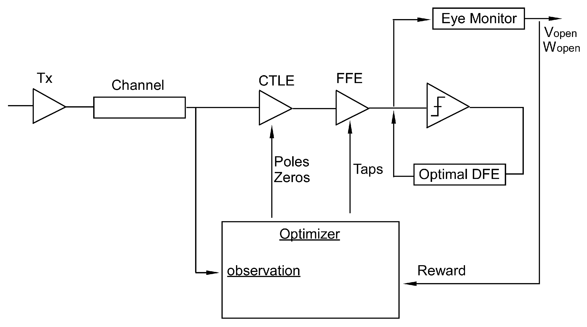
Figure 7 shows an example experiment setup with PySerDes integrated in an openAI Gym [42] environment. The experimental setup involves a 15-dB@Nyquist loss ISI channel and an eight-tap FFE, a one-stage CTLE and a 15-tap DFE. In training the agent tunes zeros and poles of the CTLE and the taps of the FFE, while the DFE taps are automatically optimized following the agent’s decision. Each start of the game resets the taps to a sub-optimal parameter set and the agent is allowed five attempts to optimized the final reward. Currently supported rewards are eye opening (EO), eye width (EW), and the eye area (EA). All costs are normalized to be circuit and technology independent.
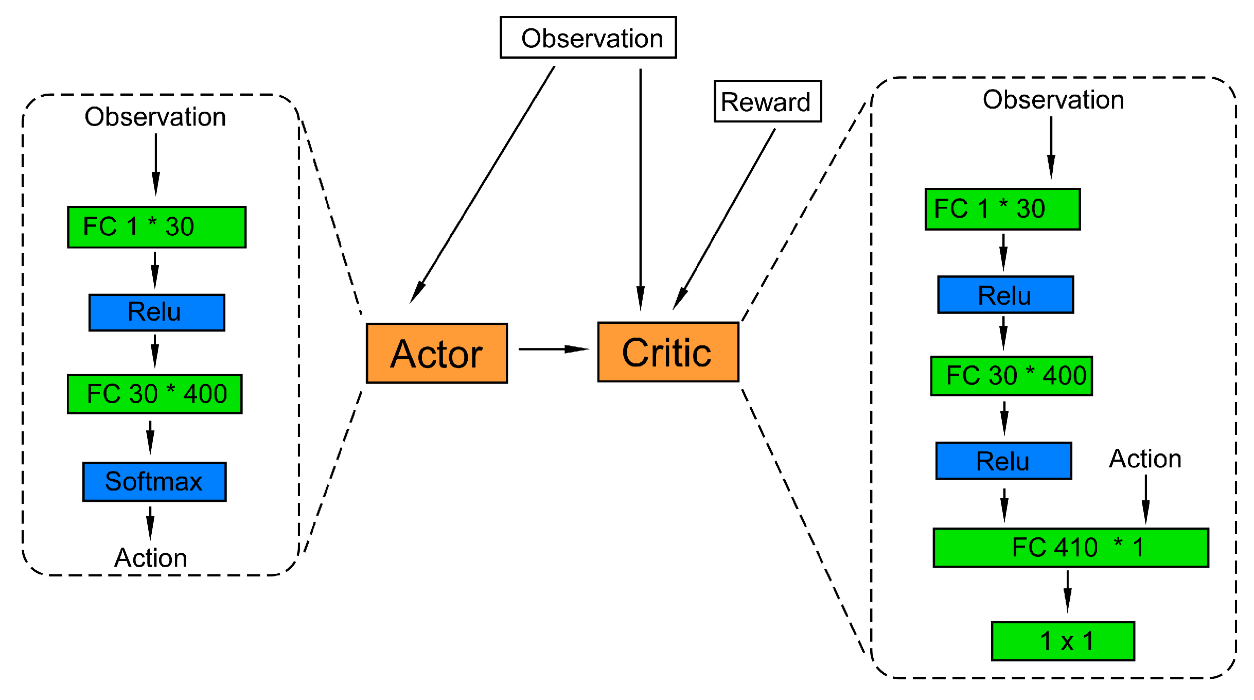
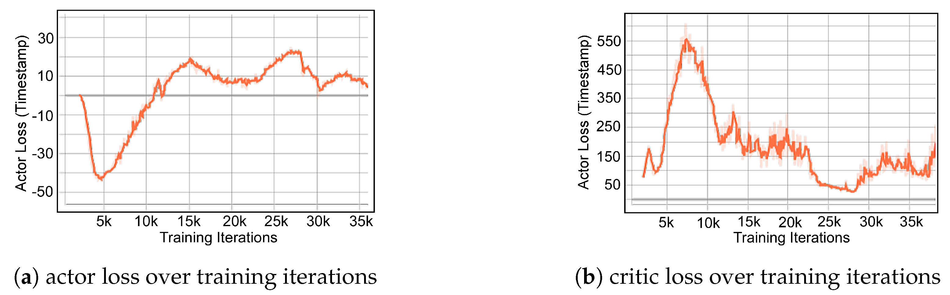
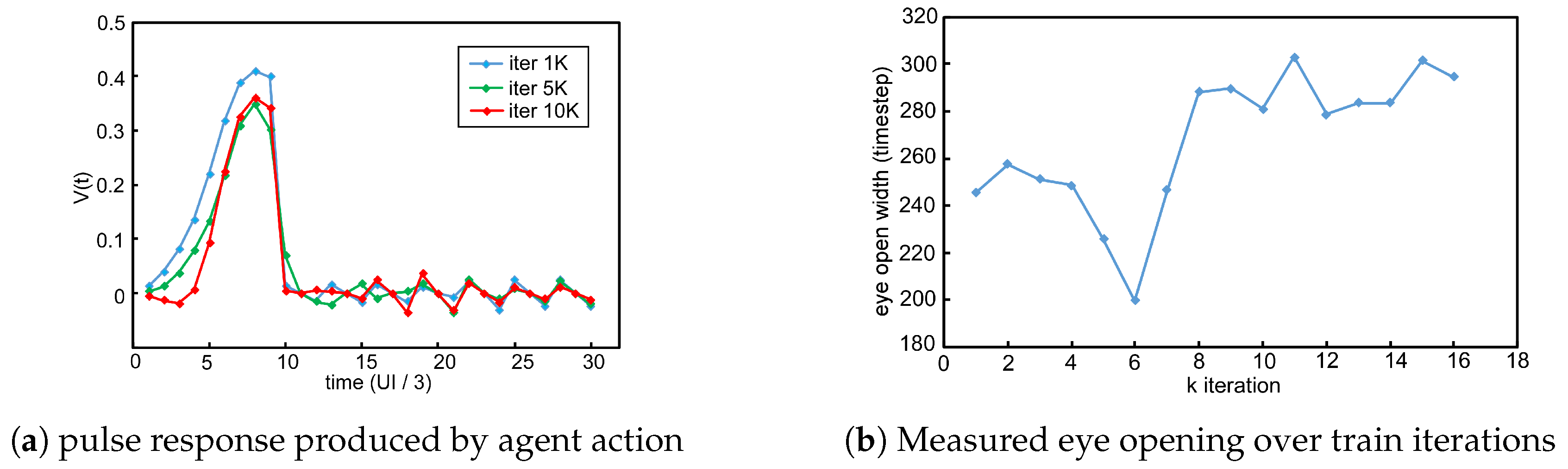
The training of the RL agent follows the method of the well-known deep deterministic policy gradient (DDPG) [43], which is a model free method providing continuous valued actions. Figure 8 illustrates the arrangement of training, and Figure 9 shows the actor and critic loss, along with the total reward the agent was able to obtain at different stages of training. To explore how the agent evolves throughout the traning Figure 10a shows the down-sampled observation at early, middle, and late stages of the training and Figure 10b shows the actual eye opening width obtained by the agent action. As can be seen in the figure, the exploration mechanism in the agent constantly explores the environment and actually learned to trade-off the height of eye opening for a better eye width. Eventually after 10 k iterations we do observe around 30% eye opening width improvement over the intialized point.
3.2. Clock Phase Recovery with ResNet
In this section we demonstrate a phase-detector (PD) logic implemented with a ResNet [44] type neural network model. Conventional phase detectors such as Alexander [45], Bang-Bang [46], and Muller–Muller [47], are derived based on certain assumptions of the data-modulated waveform, which depends on channel loss, equalizer taps, and even circuit parameters. In ResNet based phase estimation, the NN model attempts to directly estimate the timing phase information from the sampled waveform, and very little assumption was made on the actual shape of the waveform.
The real use of such a model can be at the time of design, where system designers explore the optimization space of the CDR system or potentially derived a complete CDR based on this detector, with the promising help of advanced network optimization tools, such as TVM [48] and GLOW [49].
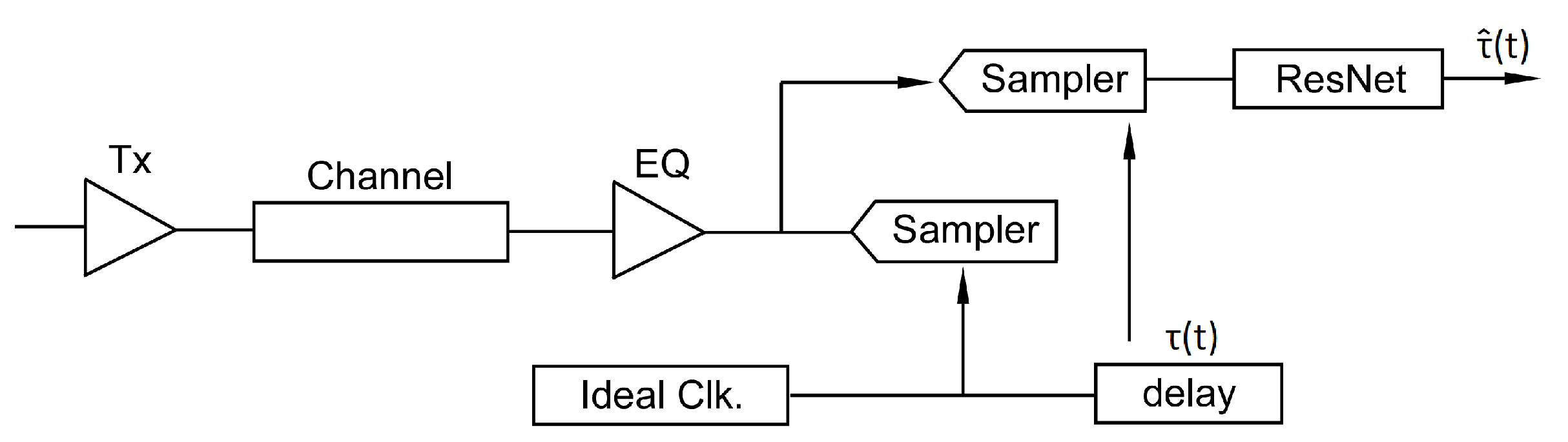
Figure 11 shows the experiment setup implemented using PySerDes and PyTorch [40]. A low loss channel and light equalization is used in this scenario. A genie sampler, one that has the maximal eye opening phase produces two times the over-sampled data reference. Another sampler, with stationary random perturbed phase offset from the genie, is used to generate the training data. The phase offset updates every 10 samples, sampled from a Gaussian distribution with zero mean and standard deviation of 1% UI.
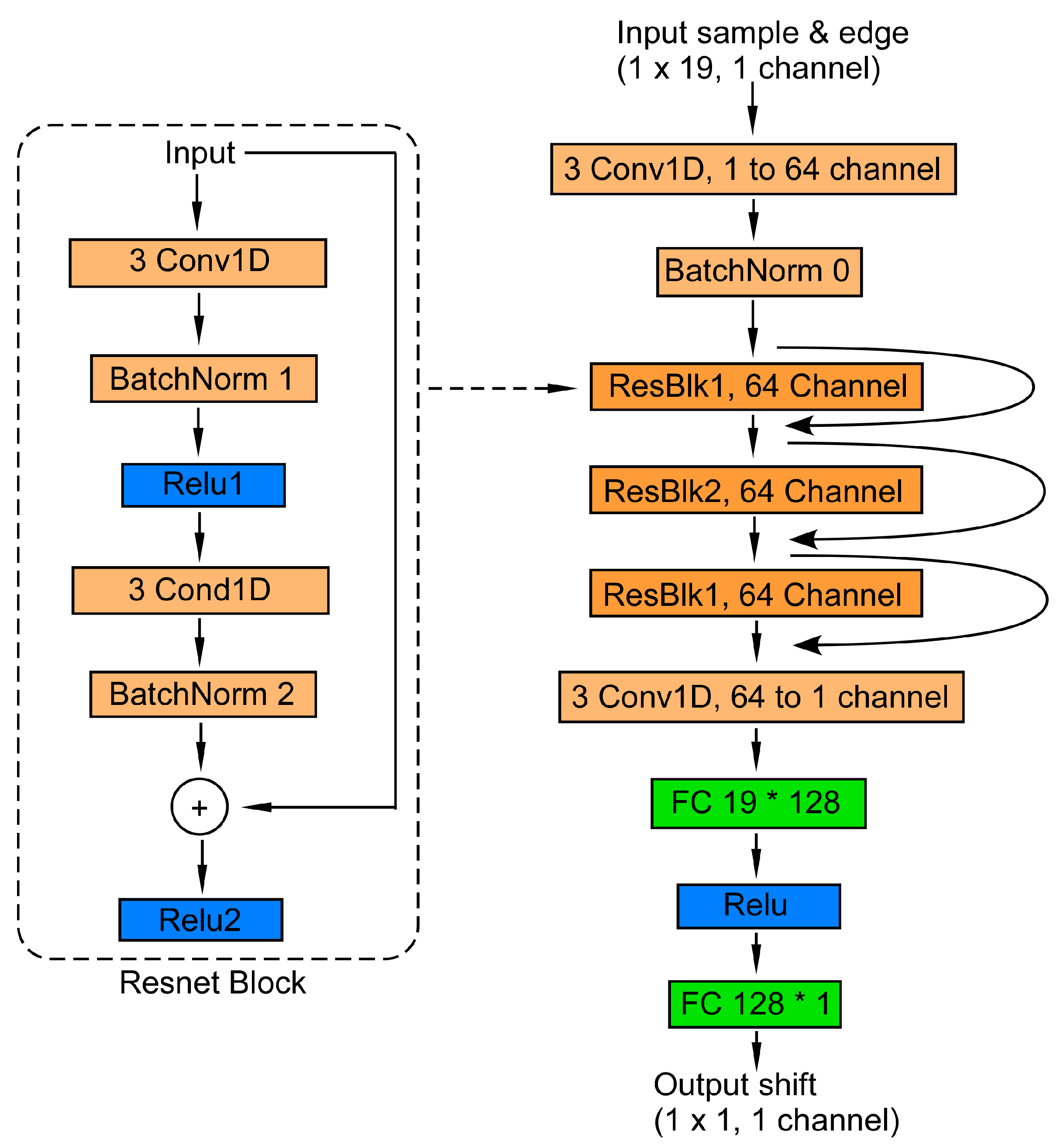
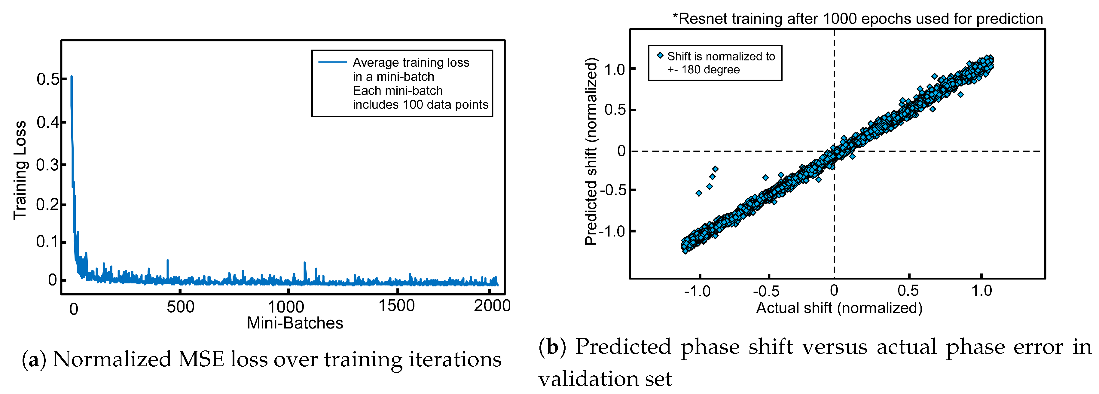
The goal of the model is to extract the perturbed phase from the noisy samples. Figure 12 shows the design of the model, with the parameter space kept intentionally small to be flexible in further development. Figure 13a shows the convergence of the training loss, which is MSE in this case, and Figure 13b shows the evaluation result. It is shown that after about 2000 iterations of training the network successfully extracts the noisy phase over the whole range of the experimental setup.
4. Future Work
System level optimization for SerDes concerns a broad range of topics from device parameters to information theoretical bounds. In this overview, some of the notable design trade-offs are discussed. The proposed PySerDes project will be publicly available under an open source license, and also has a long roadmap for expansion. Firstly, more circuit related models will be incorporated, especially supporting SPICE models and common mixed signal architectures. Meanwhile, more evaluations against industry metrics will be performed on the potential of using novel algorithms and schemes in SerDes systems. Additionally, more powerful models, and a wider variety of models will be trained and integrated into the framework to enable further explorations.
5. Conclusions
In this work, an overview of the demands and challenges in system level design of SerDes systems is provided. In particular, the designs of equalization and clocking schemes are discussed and analyzed. Finally, a python-based open framework is proposed to facilitate system level model explorations and utilization of recent advances in scientific computing and machine learning methods.
Author Contributions
Writing-original draft preparation, S.S. and Y.S.; Conceptualization, S.S. and Y.S.; Software, S.S., and Y.S.; Methodology, S.S.; Visualization, Y.S.; Validation, S.S.
Funding
This research received no external funding
Acknowledgments
The work presented in this paper was partly done while the authors were graduate students with the Departments of Electrical Engineering and Computer Science at University of Michigan, Ann Arbor.
Conflicts of Interest
The authors declare no conflict of interest.
Abbreviations
The following abbreviations are used in this manuscript:
| ADC | analog-to-digital converter |
| ADPLL | all digital phase locked loop |
| CDR | clock data recovery |
| CMOS | complementary metal–oxide–semiconductor |
| CNN | convolutional neural network |
| CTLE | continous time linear equalizer |
| DFE | decision feedback equalizer |
| DCD | duty cycle distortion |
| DDPG | deep deterministic policy gradient |
| EA | eye area |
| EO | eye opening |
| EW | eye width |
| FFE | feedforward equalizer |
| GPU | graphics processing unit |
| HPC | high performance computing |
| ISI | inter-symbol interference |
| ISF | impulse sensitivity function |
| MFB | matched filter bound |
| ML | machine learning |
| MMSE | minimum mean square error |
| MSE | mean square error |
| PLL | phase locked loop |
| RL | reinforcement Learning |
| RNN | recurrent neural network |
| RT | rise time |
| RX | receiver |
| SerDes | serializer/deserializer |
| SNDR | signal noise distortion ratio |
| SNR | signal-to-noise ratio |
| SR | supply rejection |
| SSN | simultaneous switching noise |
| TX | transmitter |
| UI | unit interval |
| VE | viterbi equalizer |
References
- Moon, Y.H.; Yoo, J.W.; Ryu, Y.S.; Kim, S.H.; Son, K.S.; Kang, J.K. A 2.41-pJ/bit 5.4-Gb/s Dual-Loop Reference-Less CDR With Fully Digital Quarter-Rate Linear Phase Detector for Embedded DisplayPort. IEEE Trans. Circuits Syst. I Regul. Pap. 2019, 66, 2907–2920. [Google Scholar] [CrossRef]
- Foley, D.; Danskin, J. Ultra-performance Pascal GPU and NVLink interconnect. IEEE Micro 2017, 37, 7–17. [Google Scholar] [CrossRef]
- Kim, D.; Park, M.; Jang, S.; Song, J.Y.; Chi, H.; Choi, G.; Choi, S.; Kim, J.; Kim, C.; Kim, K.; et al. 23.2 A 1.1 V 1ynm 6.4 Gb/s/pin 16Gb DDR5 SDRAM with a Phase-Rotator-Based DLL, High-Speed SerDes and RX/TX Equalization Scheme. In Proceedings of the 2019 IEEE International Solid-State Circuits Conference-(ISSCC), San Francisco, CA, USA, USA, 17–21 February 2019; pp. 380–382. [Google Scholar]
- Lee, P.H.; Jang, Y.C. A 3Gbps/Lane MIPI D-PHY Transmission Buffer Chip. IEICE Trans. Fundam. Electron. Commun. Comput. Sci. 2019, 102, 783–787. [Google Scholar] [CrossRef]
- Hudner, J.; Carey, D.; Casey, R.; Hearne, K.; Neto, P.W.d.A.F.; Chlis, I.; Erett, M.; Poon, C.F.; Laraba, A.; Zhang, H.; et al. A 112Gb/s PAM4 wireline receiver using a 64-way time-interleaved SAR ADC in 16 nm FinFET. In Proceedings of the 2018 IEEE Symposium on VLSI Circuits, Honolulu, HI, USA, 18–22 June 2018; pp. 47–48. [Google Scholar]
- Dittrich, M.; Heinig, A.; Hopsch, F. Electrical Characterization of a High Speed HBM Interface for a Low Cost Interposer. In Proceedings of the 2018 IEEE 68th Electronic Components and Technology Conference (ECTC), San Diego, CA, USA, 29 May–1 June 2018; pp. 2068–2073. [Google Scholar]
- Hwang, K.D.; Kim, B.; Byeon, S.Y.; Kim, K.Y.; Kwon, D.H.; Lee, H.B.; Lee, G.I.; Yoon, S.S.; Cha, J.Y.; Jang, S.Y.; et al. A 16 Gb/s/pin 8 Gb GDDR6 DRAM with bandwidth extension techniques for high-speed applications. In Proceedings of the 2018 IEEE International Solid-State Circuits Conference-(ISSCC), San Francisco, CA, USA, 11–15 February 2018; pp. 210–212. [Google Scholar]
- Dally, W.J.; Dally, W.J.; Poulton, J.W. Digital Systems Engineering; Cambridge University Press: Cambridge, UK, 1998. [Google Scholar]
- Bulzacchelli, J.F. Equalization for electrical links: Current design techniques and future directions. IEEE Solid-State Circuits Mag. 2015, 7, 23–31. [Google Scholar] [CrossRef]
- Hsieh, M.t.; Sobelman, G.E. Architectures for multi-gigabit wire-linked clock and data recovery. IEEE Circuits Syst. Mag. 2008, 8, 45–57. [Google Scholar] [CrossRef]
- Zheng, K.; Frans, Y.; Ambatipudi, S.L.; Asuncion, S.; Reddy, H.T.; Chang, K.; Murmann, B. An Inverter-Based Analog Front-End for a 56-Gb/s PAM-4 Wireline Transceiver in 16-nm CMOS. IEEE Solid-State Circuits Lett. 2018, 1, 249–252. [Google Scholar] [CrossRef]
- Palermo, S. ECEN 720 Course Resource. Available online: http://ece.tamu.edu/~spalermo/ecen720.html (accessed on 30 September 2019).
- Bergmans, J.W. Digital Baseband Transmission and Recording; Springer Science & Business Media: Berlin, Gremnay, 2013. [Google Scholar]
- Proesel, J.E.; Dickson, T.O. A 20-Gb/s, 0.66-pJ/bit serial receiver with 2-stage continuous-time linear equalizer and 1-tap decision feedback equalizer in 45nm SOI CMOS. In Proceedings of the 2011 IEEE Symposium on VLSI Circuits-Digest of Technical Papers, Honolulu, HI, USA, 15–17 June 2011; pp. 206–207. [Google Scholar]
- Song, S.; Choo, K.D.; Chen, T.; Jang, S.; Flynn, M.P.; Zhang, Z. A maximum-likelihood sequence detection powered ADC-based serial link. IEEE Trans. Circuits Syst. I Regul. Pap. 2017, 65, 2269–2278. [Google Scholar] [CrossRef]
- Yueksel, H.; Braendli, M.; Burg, A.; Cherubini, G.; Cideciyan, R.D.; Francese, P.A.; Furrer, S.; Kossel, M.; Kull, L.; Luu, D.; et al. Design Techniques for High-Speed Multi-Level Viterbi Detectors and Trellis-Coded-Modulation Decoders. IEEE Trans. Circuits Syst. I Regul. Pap. 2018, 65, 3529–3542. [Google Scholar] [CrossRef]
- Gray, P.R.; Hurst, P.J.; Lewis, S.H.; Meyer, R.G. Anal. Des. Analog Integr. Circuits; John Wiley & Sons: Hoboken, NJ, USA, 2009. [Google Scholar]
- Kim, J.; Leibowitz, B.S.; Jeeradit, M. Impulse sensitivity function analysis of periodic circuits. In Proceedings of the 2008 IEEE/ACM International Conference on Computer-Aided Design, San Jose, CA, USA, 10–13 November 2008; IEEE Press: Piscataway, NJ, USA, 2008; pp. 386–391. [Google Scholar]
- Casper, B. Clocking wireline systems: An overview of wireline design techniques. IEEE Solid-State Circuits Mag. 2015, 7, 32–41. [Google Scholar] [CrossRef]
- Balestrieri, E.; Picariello, F.; Rapuano, S.; Tudosa, I. Review on jitter terminology and definitions. Measurement 2019, 145, 264–273. [Google Scholar] [CrossRef]
- Hyun, C.; Ko, H.; Chae, J.H.; Park, H.; Kim, S. A 20Gb/s Dual-Mode PAM4/NRZ Single-Ended Transmitter with RLM Compensation. In Proceedings of the 2019 IEEE International Symposium on Circuits and Systems (ISCAS), Sapporo, Japan, 26–29 May 2019; pp. 1–4. [Google Scholar]
- Best, R.E. Phase Locked Loops: Design, Simulation, and Applications; McGraw-Hill Professional: Pennsylvania, PA, USA, 2007. [Google Scholar]
- Park, H.; Song, J.; Lee, Y.; Sim, J.; Choi, J.; Kim, C. 23.3 A 3-bit/2UI 27Gb/s PAM-3 Single-Ended Transceiver Using One-Tap DFE for Next-Generation Memory Interface. In Proceedings of the 2019 IEEE International Solid-State Circuits Conference-(ISSCC), San Francisco, CA, USA, 17–21 February 2019; pp. 382–384. [Google Scholar]
- LaCroix, M.A.; Wong, H.; Liu, Y.H.; Ho, H.; Lebedev, S.; Krotnev, P.; Nicolescu, D.A.; Petrov, D.; Carvalho, C.; Alie, S.; et al. 6.2 A 60Gb/s PAM-4 ADC-DSP Transceiver in 7nm CMOS with SNR-Based Adaptive Power Scaling Achieving 6.9 pJ/b at 32dB Loss. In Proceedings of the 2019 IEEE International Solid-State Circuits Conference-(ISSCC), San Francisco, CA, USA, 17–21 February 2019; pp. 114–116. [Google Scholar]
- Kim, J. Advanced modeling and simulation of state-of-the-art high-speed I/O interfaces. In Proceedings of the IEEE 2014 Custom Integrated Circuits Conference, IEEE, San Jose, CA, USA, 15–17 September 2014; pp. 1–122. [Google Scholar]
- Ren, J.; Oh, D.; Chang, S. High-speed I/O jitter modeling methodologies. In Proceedings of the IEEE 19th Topical Meeting on Electrical Performance of Electronic Packaging and Systems, Austin, TX, USA, 25–27 October 2010; pp. 113–116. [Google Scholar]
- Abadi, M.; Barham, P.; Chen, J.; Chen, Z.; Davis, A.; Dean, J.; Devin, M.; Ghemawat, S.; Irving, G.; Isard, M.; et al. Tensorflow: A system for large-scale machine learning. In Proceedings of the 12th USENIX Symposium on Operating Systems Design and Implementation (OSDI 16), Savannah, GA, USA, 2–4 November 2016; pp. 265–283. [Google Scholar]
- Binkert, N.; Beckmann, B.; Black, G.; Reinhardt, S.K.; Saidi, A.; Basu, A.; Hestness, J.; Hower, D.R.; Krishna, T.; Sardashti, S.; et al. The gem5 simulator. ACM Sigarch Comput. Archit. News 2011, 39, 1–7. [Google Scholar] [CrossRef]
- Karandikar, S.; Mao, H.; Kim, D.; Biancolin, D.; Amid, A.; Lee, D.; Pemberton, N.; Amaro, E.; Schmidt, C.; Chopra, A.; et al. FireSim: FPGA-accelerated cycle-exact scale-out system simulation in the public cloud. In Proceedings of the 45th Annual International Symposium on Computer Architecture, Los Angeles, CA, USA, 2–6 June 2018; IEEE Press: Piscataway, NJ, USA, 2018; pp. 29–42. [Google Scholar]
- Chong, K.H.A.; Avula, V.; Liang, L.; Pam, S.; Mansour, M.; Rao, F. IBIS AMI modeling of retimer and performance analysis of retimer based active serial links. Des. Con. 2014. Available online: https://www.keysight.com/upload/cmc_upload/All/8_WE5Combined_IBISAMIModelingofRetimer.pdf (accessed on 30 September 2019).
- Jones, E.; Oliphant, T.; Peterson, P. SciPy: Open source scientific tools for Python. 2014. Available online: http://www.scipy.org (accessed on 30 September 2019).
- Chen, Y.; Harms, P.; Mittra, R.; Beyene, W. Analysis of complex electronic packages with the use of using the FDTD/touchstone hybrid technique. Microw. Opt. Technol. Lett. 1996, 12, 313–315. [Google Scholar] [CrossRef]
- Klöckner, A.; Pinto, N.; Lee, Y.; Catanzaro, B.; Ivanov, P.; Fasih, A. PyCUDA and PyOpenCL: A scripting-based approach to GPU run-time code generation. Parallel Comput. 2012, 38, 157–174. [Google Scholar] [CrossRef]
- Perrott, M.H. Fractional-N Frequency Synthesizer Design Using The PLL Design Assistant and CppSim Programs. CppSim Tutor. Man. 2008. Available online: http://cppsim.org/Tutorials/synthesizer_tutorial.pdf (accessed on 30 September 2019).
- Bertsekas, D.P.; Scientific, A. Convex Optimization Algorithms; Athena Scientific Belmont: Belmont, MA, USA, 2015. [Google Scholar]
- Bergstra, J.; Yamins, D.; Cox, D.D. Hyperopt: A python library for optimizing the hyperparameters of machine learning algorithms. In Proceedings of the 12th Python in Science Conference, Citeseer, Austin, TX, USA, 24–29 June 2013; pp. 13–20. [Google Scholar]
- Bishop, C.M. Pattern Recognition and Machine Learning; Springer: Berlin, Germany, 2006. [Google Scholar]
- Deng, J.; Dong, W.; Socher, R.; Li, L.J.; Li, K.; Fei-Fei, L. Imagenet: A large-scale hierarchical image database. In Proceedings of the 2009 IEEE Conference on Computer Vision and Pattern Recognition, Miami, FL, USA, 20–25 June 2009; pp. 248–255. [Google Scholar]
- Nguyen, T.; Lu, T.; Wu, K.; Schutt-Aine, J. Fast Transient simulation of High-Speed Channels using Recurrent Neural Network. arXiv 2019, arXiv:1902.02627. [Google Scholar]
- Paszke, A.; Gross, S.; Chintala, S.; Chanan, G.; Yang, E.; DeVito, Z.; Lin, Z.; Desmaison, A.; Antiga, L.; Lerer, A. Automatic Differentiation in Pytorch. 2017. Available online: https://openreview.net/forum?id=BJJsrmfCZ (accessed on 30 September 2019).
- Li, Y. Deep reinforcement learning: An overview. arXiv 2017, arXiv:1701.07274. [Google Scholar]
- Brockman, G.; Cheung, V.; Pettersson, L.; Schneider, J.; Schulman, J.; Tang, J.; Zaremba, W. Openai gym. arXiv 2016, arXiv:1606.01540. [Google Scholar]
- Lillicrap, T.P.; Hunt, J.J.; Pritzel, A.; Heess, N.; Erez, T.; Tassa, Y.; Silver, D.; Wierstra, D. Continuous control with deep reinforcement learning. arXiv 2015, arXiv:1509.02971. [Google Scholar]
- He, K.; Zhang, X.; Ren, S.; Sun, J. Deep residual learning for image recognition. In Proceedings of the IEEE Conference on Computer Vision and Pattern Recognition, Las Vegas, NV, USA, 26 June–1 July 2016; pp. 770–778. [Google Scholar]
- Razavi, B. Monolithic Phase-Locked Loops and Clock Recovery Circuits: Theory and Design; John Wiley & Sons: Hoboken, NJ, USA, 1996. [Google Scholar]
- Da Dalt, N. Markov chains-based derivation of the phase detector gain in bang-bang PLLs. IEEE Trans. Circuits Syst. II Express Briefs 2006, 53, 1195–1199. [Google Scholar] [CrossRef]
- Dokania, R.; Kern, A.; He, M.; Faust, A.; Tseng, R.; Weaver, S.; Yu, K.; Bil, C.; Liang, T.; O’Mahony, F. 10.5 A 5.9 pJ/b 10Gb/s serial link with unequalized MM-CDR in 14nm tri-gate CMOS. In Proceedings of the 2015 IEEE International Solid-State Circuits Conference-(ISSCC) Digest of Technical Papers, San Francisco, CA, USA, 22–26 February 2015; pp. 1–3. [Google Scholar]
- Chen, T.; Moreau, T.; Jiang, Z.; Zheng, L.; Yan, E.; Shen, H.; Cowan, M.; Wang, L.; Hu, Y.; Ceze, L.; et al. {TVM}: An automated end-to-end optimizing compiler for deep learning. In Proceedings of the 13th USENIX Symposium on Operating Systems Design and Implementation (OSDI 18), Carlsbad, CA, USA, 8–10 October 2018; pp. 578–594. [Google Scholar]
- Rotem, N.; Fix, J.; Abdulrasool, S.; Catron, G.; Deng, S.; Dzhabarov, R.; Gibson, N.; Hegeman, J.; Lele, M.; Levenstein, R.; et al. Glow: Graph lowering compiler techniques for neural networks. arXiv 2018, arXiv:1805.00907. [Google Scholar]
Figure 1.
Example SerDes applications across applications and data rates.

Figure 2.
System model of a typical SerDes system .

Figure 3.
Insertion loss of a typical channel [12].
Figure 3.
Insertion loss of a typical channel [12].

Figure 4.
Inter-symbol interference (ISI) characterized on time and frequency domain.

Figure 5.
Example implementations of a DFE (top) and a CTLE (bottom).

Figure 6.
Python-based SerDes (PySerDes) Library Overview. phase lock loops (PLLs).

Figure 7.
Experiment setup for reinforcement learning (RL) agent training.

Figure 8.
Design of the RL agent for equalizer tuning.

Figure 9.
Convergence during the traning of the RL agents.

Figure 10.
Observed waveform and metrics from the training process of RL.

Figure 11.
Experiment setup for clock data recovery (CDR) training.

Figure 12.
Design of the ResNet structure for phase extraction.

Figure 13.
Evaluation of the ResNet phase extractor.

© 2019 by the authors. Licensee MDPI, Basel, Switzerland. This article is an open access article distributed under the terms and conditions of the Creative Commons Attribution (CC BY) license (http://creativecommons.org/licenses/by/4.0/).
Share and Cite
MDPI and ACS Style
Song, S.; Sui, Y. System Level Optimization for High-Speed SerDes: Background and the Road Towards Machine Learning Assisted Design Frameworks. Electronics 2019, 8, 1233. https://doi.org/10.3390/electronics8111233
AMA Style
Song S, Sui Y. System Level Optimization for High-Speed SerDes: Background and the Road Towards Machine Learning Assisted Design Frameworks. Electronics. 2019; 8(11):1233. https://doi.org/10.3390/electronics8111233
Chicago/Turabian StyleSong, Shiming, and Yu Sui. 2019. "System Level Optimization for High-Speed SerDes: Background and the Road Towards Machine Learning Assisted Design Frameworks" Electronics 8, no. 11: 1233. https://doi.org/10.3390/electronics8111233
Note that from the first issue of 2016, this journal uses article numbers instead of page numbers. See further details here.