Quantitative Analysis of Multistage Switching Networks for Embedded Programmable Devices
by
 ,
,
Francesco Renzini
1,* ,
,
Matteo Cuppini
1,
Claudio Mucci
2,
Eleonora Franchi Scarselli
1 and
Roberto Canegallo
2 1
ARCES-DEI, University of Bologna, Viale Carlo Pepoli 3/2, 40123 Bologna, Italy
2
STMicroelectronics, 20864 Agrate Brianza, Italy
*
Author to whom correspondence should be addressed.
Electronics 2019, 8(3), 272; https://doi.org/10.3390/electronics8030272
Submission received: 29 January 2019
/
Revised: 21 February 2019
/
Accepted: 25 February 2019
/
Published: 1 March 2019
(This article belongs to the Special Issue Recent Advances in Field-Programmable Logic and Applications)
Abstract
:This paper analyzes the properties of a class of congestion-free multistage switching networks (MSSNs) are butterfly-based and suitable for embedded programmable devices, which require sustaining static multicast connectivity. These MSSNs are fully synthesizable and enable the design of programmable IPs with typical size in the order of 1 KLUT, coupling flexibility with fast turn-around time. The non-blocking property for static connection of this class of MSSN is discussed. Our analysis shows pros and cons of adopting radix-2 or radix-4 MSSN structures, as well as the impact of bypass-paths to make the network fully hierarchical and locality-aware thanks also to a dedicated programming strategy. Implementation experiments carried out on STM CMOS 65 nm technology show the availability of various area-speed trade-offs, resulting in a range of ≃2× in frequency and a range of ≃ in area. Depending on the specific application-field, an optimal interconnect definition is thus achieved without compromising the routability properties. In this respect, the paper proposes a simplified application-driven model for evaluation of the best MSSN, including bypass-adoption and radix selection.
1. Introduction
Nowadays, embedded programmable logic devices (ePLDs) can be applied in system-on-a-chip (SoC) designs to increase flexibility, widen their market, and curb soaring nonrecurring engineering (NRE) costs [1,2,3,4,5,6]. Embedded Field Programmable Gate Arrays (eFPGAs) are a class of ePLD that can provide computational advantages in terms of Giga Operations Per Second/mm (GOPS/mm) over processors and Digital Signal Processors (DSPs) [7], although several well-known drawbacks, mainly in terms of area, have historically restricted their use on the market of SoCs. In fact, the tight relationship between costs and silicon-area has historically driven the SoC market, especially for mid- to high-volume applications. For that reason, eFPGA cores must provide added value to the system but only take up a small percentage of the overall device area. To be effective we can estimate the target computational complexity around 1–10 KGates. For that, the typical size of such device can be evaluated in the order of ≃1 KLUT, eventually enhanced by hardwired DSP accelerators, hence the target application is not high-density computation but simple Finite State Machines (FSMs). An application domain of such a class of small-size eFPGA is the Smart-Power world that is demanding “intelligence” to improve efficiency [8]. Power applications, e.g., motion- and lighting-control, are mostly based on a control-driven paradigm which leverages simple controllers—e.g., finite-state machines (FSMs)—with few inlets/outlets and states. To be easily embedded in a more complex system, the eFPGA is designed to be fully synthesizable—hence following a soft-core approach. This enables the possibility to optimize the eFPGA template by using standard implementation flow, based on standard cells, thus proving portability to different technology nodes. This feature allows the implementation of the device on CMOS technologies, as well on BCD (Bipolar, CMOS, and DMOS) technologies tailored for Smart- Power applications. The eFPGA soft-core approach provides easier floorplan in system-on-chip where high-power devices and analog circuits take up the majority of the area since it allows the digital section to fully adapt among other parts, contrary to the eFPGA hard-macros approach. It is important to observe that the different size of such a device with respect to state-of-the-art commercial FPGA, which is nowadays easily reaching the million-gate target, and is justified and required by the strongly different economic model, as shown in [3]. In fact, wide bit-level programmability, such as that one provided by FPGAs, is justified only in case of many low-volume applications (NRE-dominated cost model).
Recent works [4,6,8,9] have shown that for eFPGA a soft-core approach can guarantee integration advantages (e.g., floorplan, technology flavors, and portability) and improved flexibility (e.g., customization of array size and availability of DSP enhancements). In [4] we introduced a template for soft-core eFPGA, analyzing the challenges and added values given by a fully synthesizable approach. Foundation of programmable routing is a multistage switching network (MSSN), a solution that enables synthesizable and flexible design, one of the key points of our approach. Since the area of MSSN typically growth with , this solution is effective only for small-size eFPGA cores. Indeed, increasing the amount of resources to be connected, the area-penalty associated to congestion-free MSSNs become unsustainable and stages/paths depopulation must be arranged [10].
This article complements [4] and is an extension of [5] where preliminary results of the analysis of MSSN as interconnect structure for small programmable IPs are discussed. Indeed, although eFPGA internal communication through the MSSN requires just static connection, a detailed analysis of the MSSN characteristics and trade-offs on eFPGA domain is missing in [4] and is the focus of the present paper. We will show both MSSN compatibility with soft-core design methodologies and its intrinsic congestion-free properties, which are analyzed for different architectural flavors.
The paper is organized as follows. Section 2 introduces the MSSNs in the eFPGA scenario also reviewing related works, while Section 3 details rules to design multicast MSSN to achieve static congestion-free connectivity. Section 4 analyses the rearrangeably non-blocking (RNB) features of the MSSN we proposed in [4], extending the analysis to other structures with the same RNB properties. Section 5 discusses the programming tool developed to configure those MSSNs. Section 6 and Section 7 quantitatively analyze congestion-free MSSNs in terms of area/speed tradeoffs for different architectural options, including radix-2 or radix-4 MSSN, as well as bypass paths. Section 8 summarizes the conclusions.
2. Related Work
Embedded FPGAs, like the larger stand-alone FPGAs, are arrays of computational logic blocks (LB) connected using programmable routing [11]. Overall efficiency of an eFPGA is deeply affected by routing, since it greatly impacts area and performances and is responsible for the efficiency of the connections [10,12]. With the growth in complexity of the target applications, research work has been spent in overcoming the penalties related to bit-level programmability and in alleviating routing congestion issues. Leveraging on Rent’s rules, hierarchical interconnects were thus proposed to diminish complexity issues, enabling reduction of the area overhead of programmable routing through local crossbars capable to connect clusters of LB [13,14,15].
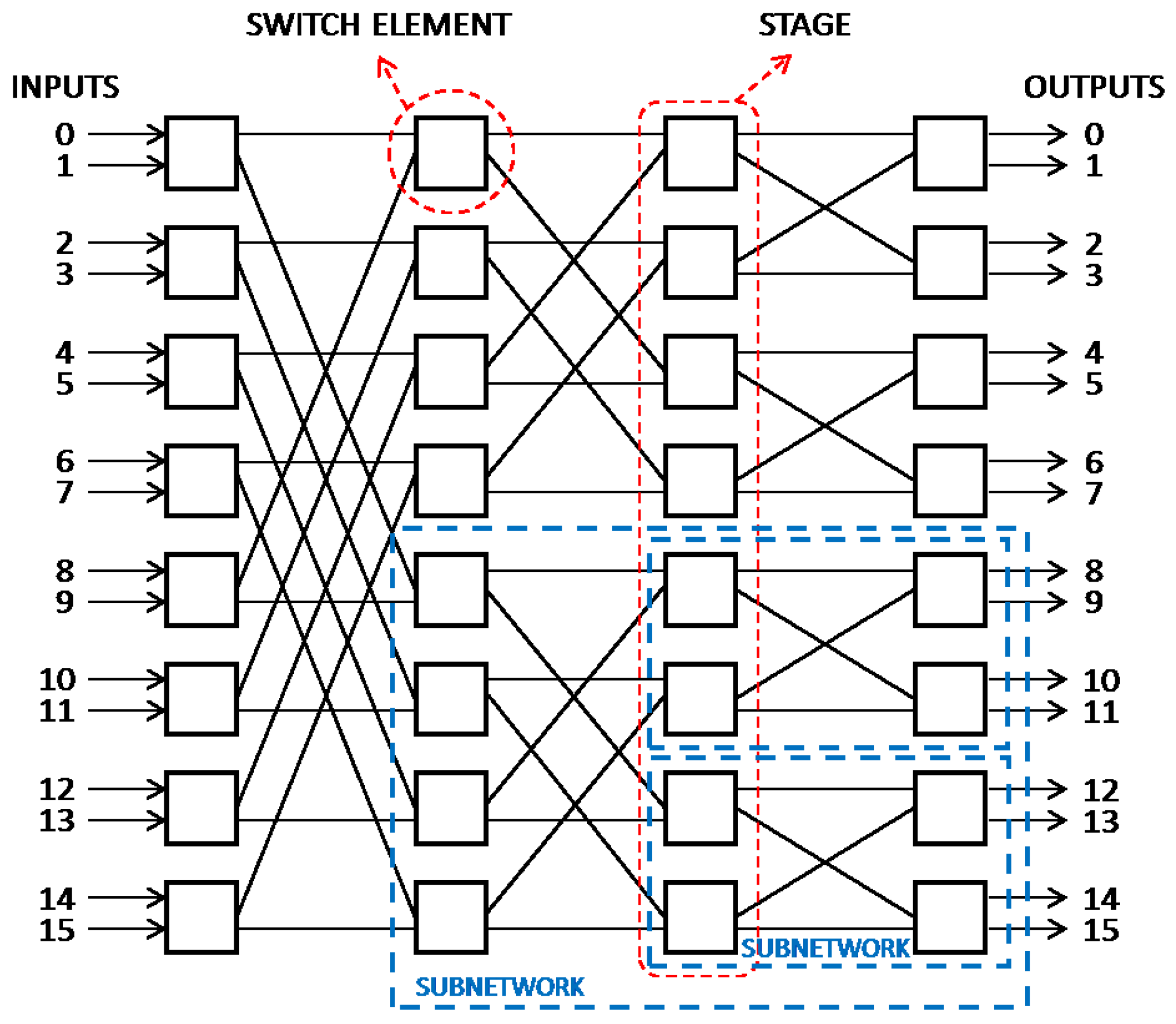
Multistage switching networks (MSSN) are a kind of hierarchical interconnection network built using many small crossbars, typically called switch elements (SE) (Figure 1).
Depending on its topology and/or its ability to perform connection between input and output ports, a MSSN can be:
- Non-blocking, if it can connect each I/O pair regardless of the existing connections on the network.
- Blocking, if it cannot connect all the requests.
Among the non-blocking networks, a network is strictly non-blocking (SNB) if any connection can be set up incrementally without the need to rearrange (i.e., reroute) any of the connections already in place, while it is rearrangeably non-blocking (RNB) if one or more existing connections may have to be rearranged to permit a new connection. All the previous definitions can be used for unicast (one-to-one), multicast (one-to-many), or broadcast (one-to-all) traffic.
MSSNs for eFPGAs must support multicast connectivity but, since circuits have static connectivity, the utilization of RNB networks is equivalent to SNB, allowing congestion-avoidance with fewer resources. In the eFPGA scenario, the application of MSSNs can provide some straightforward advantages:
- The modularity of the network potentially adapts to a soft-core approach. Each SE can be either implemented by standard-cells or optimized at circuit level as a single coarse-grained cell, without affecting synthesizability.
- MSSN routability properties improve the flexibility of eFPGA design, allowing architectural variations (e.g., size and I/Os number) without the need of specific skills in congestion analysis and prevention.
- The routability analysis is simplified, since the blocking properties of an MSSN are well-defined and predictable in terms of topology, as discussed in Section 4.
Some examples of application of hierarchical interconnects in eFPGA are found in the literature. M2000 (Abound Logic) proposed an MSSN with local crossbars based on a Clos network [16], while Leopard Logic proposed a butterfly-based hierarchical network [17]. In [10,18] an MSSN based on butterfly topology is discussed with depopulation of the upper stages of the network and an isomorphic transformation to solve the radix-boundary problem [19], a limiting factor of MSSN in the field of FPGAs. Nevertheless, area saving is balanced by the fact that this network is no more proven to be RNB, although authors indicates the availability of enough bandwidth based on Rent’s rule. Another example of multi-level interconnect dimentioning based on Rent’s rule applied to logarithmic paths is provided by [20], which overcomes boundary-radix issue by adding shortcuts and staggering.
In [4] we proposed an eFPGA template core with MSSN-based interconnect: all the performance analysis and results refer to the overall eFPGA core, composed of both logic blocks and interconnect. For the proposed eFPGA the utilization of a MSSN to realize the interconnect structure represented a key enabler, but not the unique aspect; a detailed analysis and exploration of a class of MSSN suitable to realize the interconnect structure of synthesizable small size programmable IPs was missing in [4] and is the goal of this paper, which extends and formalizes preliminary results discussed in the M. Cuppini PhD Thesis [5]. The RNB feature of the class of MSSN we propose is discussed in Section 4, whereas a dedicated configuration strategy allows to achieve a straight-as-possible policy in order to minimize the boundary-radix problem, as discussed in Section 5. Different architectural options, including values of radix and level of bypass exploitation are analyzed and compared showing area-frequency trade-offs in Section 6 and Section 7 [14,15].
3. Multicast Multistage Switching Networks
The field of RNB multicast networks is quite wide [21], but for eFPGA application we consider architectures capable to guarantee a small area overhead for a number of I/Os that can reach some thousands of points with reduced timing penalties. For that, among all the MSSNs applied in telecommunication fields [21,22,23,24], the starting point for PLD domain are the Banyan networks [25], and their topological equivalent versions [25,26] (e.g., Omega, Shuffle, Butterfly), since they are a class of low-latency multistage networks.
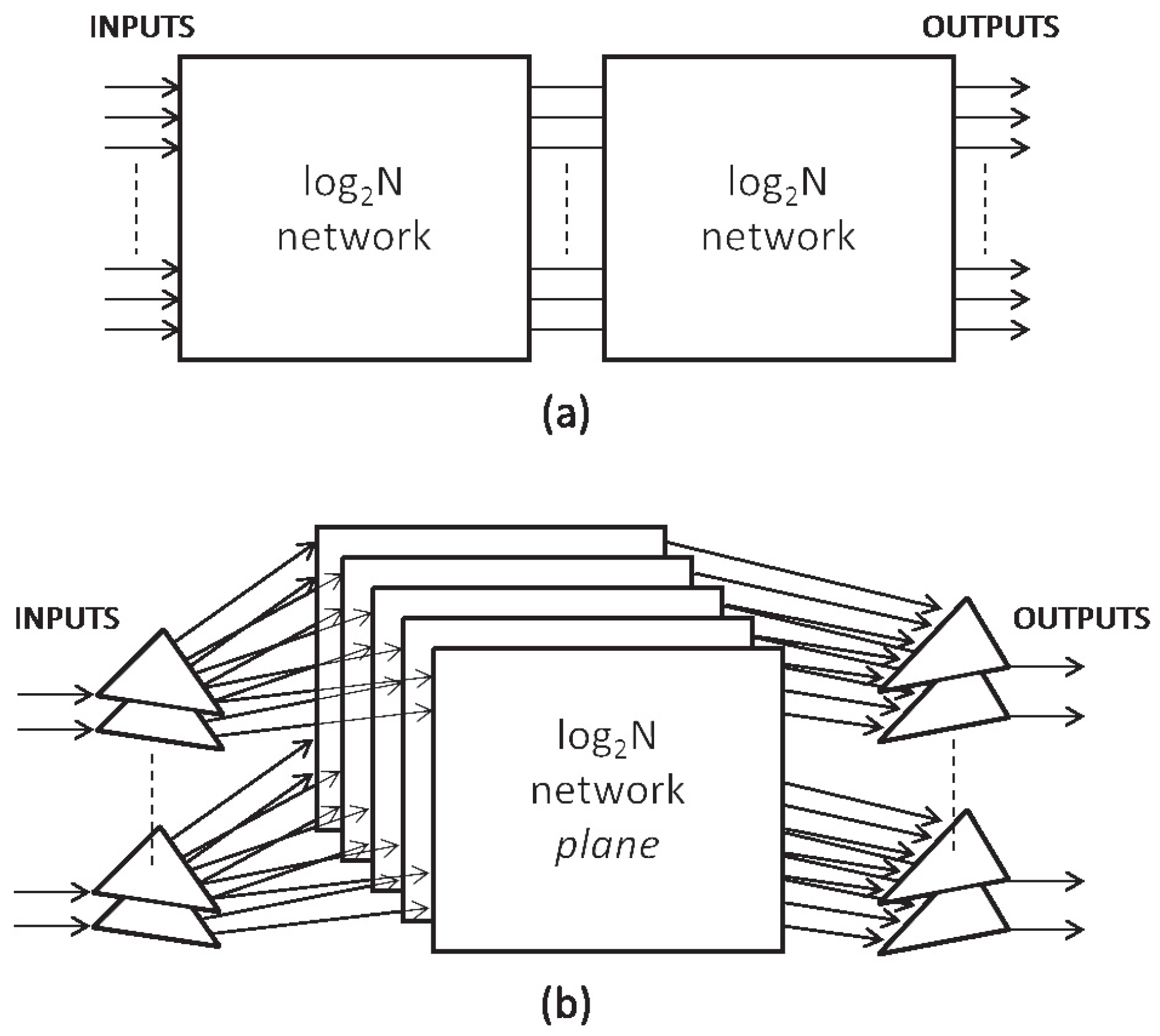
Banyan networks, as shown in Figure 1 for , are built using switch elements organized in stages [27], and for this reason they are also called -networks [28]. Thanks to low-latency and recursive architecture, since an N-input network can be recursively decomposed into two sub-networks, and so on (as shown in Figure 1), Banyan networks are very attractive MSSNs [25]. The main drawback is that Banyan networks are blocking, also for unicast traffic. To obtain RNB features, Banyan networks need additional resources to the baseline structure: the resulting networks are called Multi- networks [28]. One such approach typically used in the literature to get an RNB network is the Horizontal Cascading (HC) of two baseline -networks (Figure 2a): Benes networks [29,30] are an example of this technique, since they are built by cascading two baseline networks back-to-back. However, the HC approach implies complex routing algorithms (due to a large amount of reconfiguration activity) [28].
As an alternative, the vertical stacking (VS) technique was introduced [27]. According to this scheme (Figure 2b), in a Vertically-Stacked MSSN (VS-MSSN) various different copies (called planes) of a baseline network are created and connected to I/Os through an input (output) stage of demultiplexers (multiplexers). As regards multicast, in [31] the condition on the number of planes p necessary to obtain RNB features in VS-MSSNs is expressed as:
where n is the number of stages of the baseline network, such that:
In [32] a class of non-blocking networks built with a combination of HC and VS was proposed. Thanks to this approach, obtained by adding x extra stages to each baseline plane, the condition for RNB unicast is proven:
This solution can lead to a reduction of the total hardware complexity, since adding x (lower than n) horizontal stages allows one to save one (or more) whole planes. Reference [32] proves Equation (3) for one-to-one connection, while [33] generalized the properties defined by [28] for vertical stacking also for multicast connection. We have intensely tested the proposed MSSN in multicast applications, without finding any unresolved conditions. From a qualitative point of view, the equivalence between horizontal and vertical decomposition finds it foundation in the fact that they are different strategies to provide the same paths multiplicity in connecting a generic input-output pair under the condition defined by (3). Simultaneously, the combination of HC and VS open the way for exploring various trade-off between hardware complexity and latency.
4. MSSN for Embedded Programmable Devices
4.1. MSSN Based on Switches
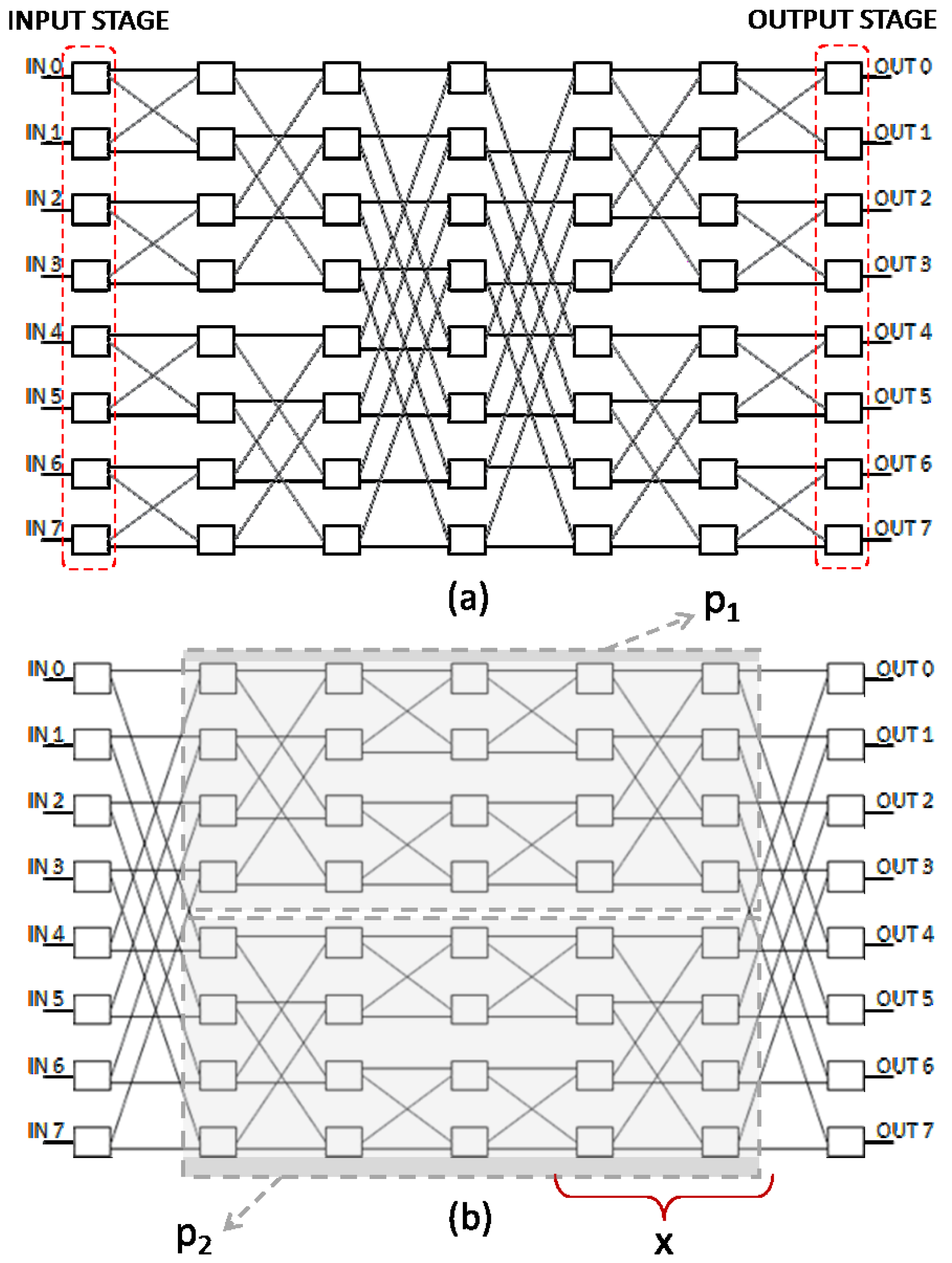
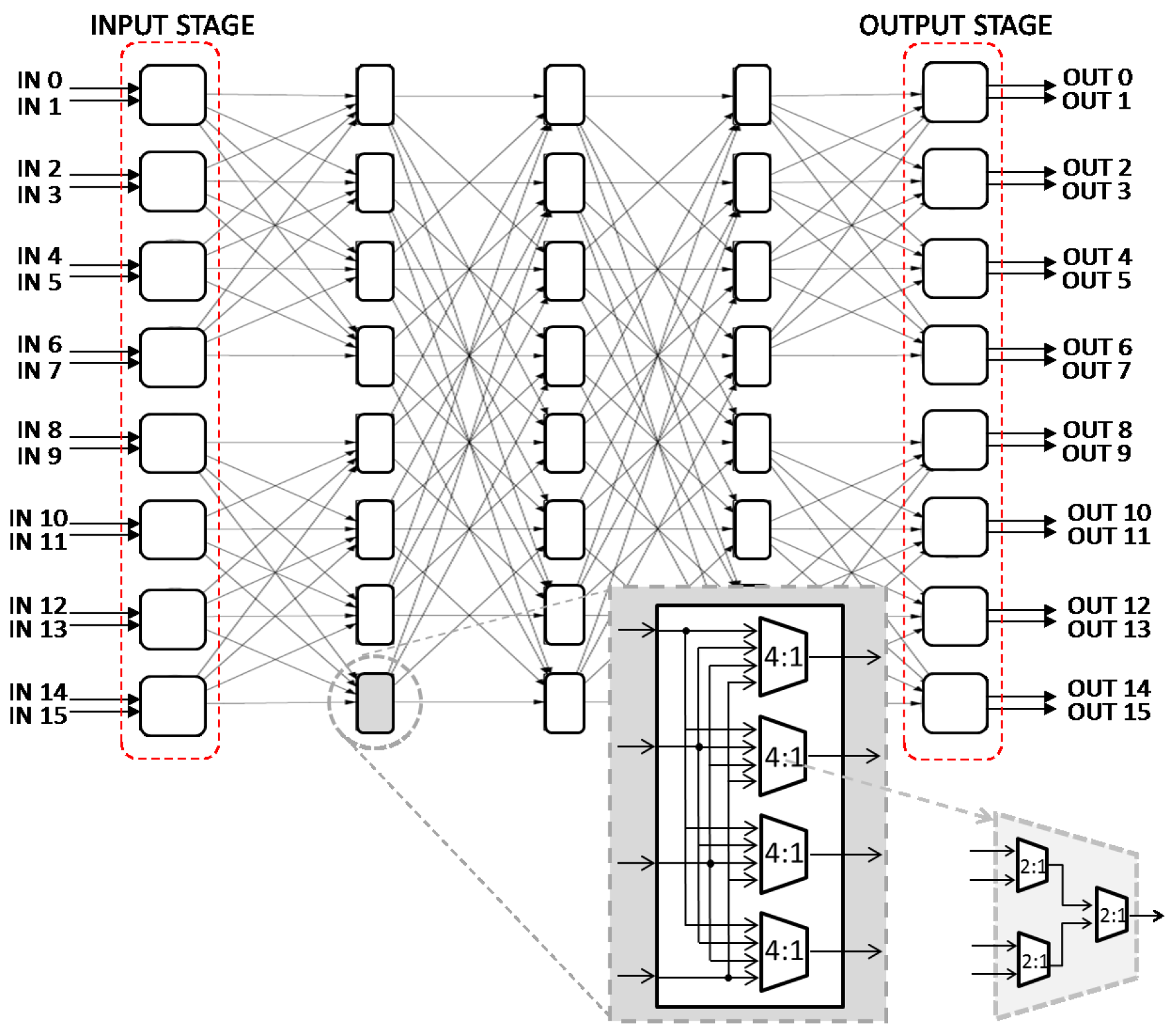
The MSSN architecture we propose in [4] features a Benes-like topology with butterfly connectivity, and is shown in Figure 3a. Based on switches, an I/Os MSSN features stages, with switch blocks per stage, so that:
Among these, one input stage (IN) composed of switches and one output stage (OUT) formed of switches are used as demultiplexing/multiplexing stages for the vertical stacking technique (see Section 3), while the remaining () middle stages (MID), each composed of switch elements, are used to form the MSSN planes. Equation (4) becomes:
This MSSN architecture (shown in Figure 3a) is topologically equivalent [34], i.e., with the same graph, to that in Figure 3b. Such a network has planes and ), each made of an Banyan network, and extra stages. Since, according to Equation (2), the stages number of a baseline network is , condition (3) becomes:
and is satisfied for any value of N with .
It must be specified that a lower number of extra stages x should suffice to satisfy condition (3), since with and , only extra stages are strictly required; such an area-penalizing choice, a complexity increase proportional to N, was made with a view to obtaining a symmetry feature that opens the way to architectural enhancement of the MSSN described in the following paragraph.
4.2. MSSN with Bypass Enhancement
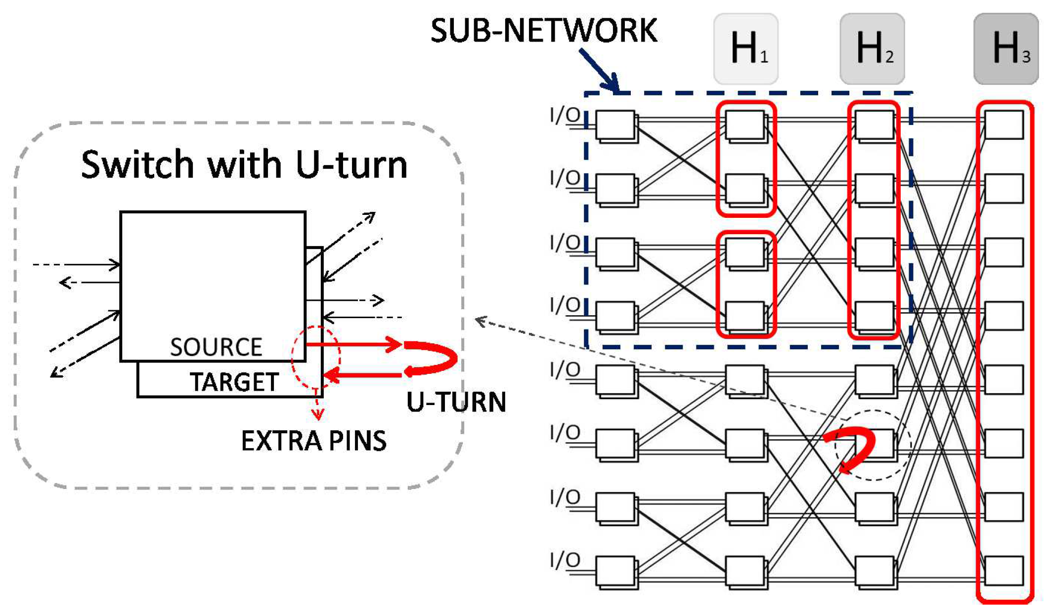
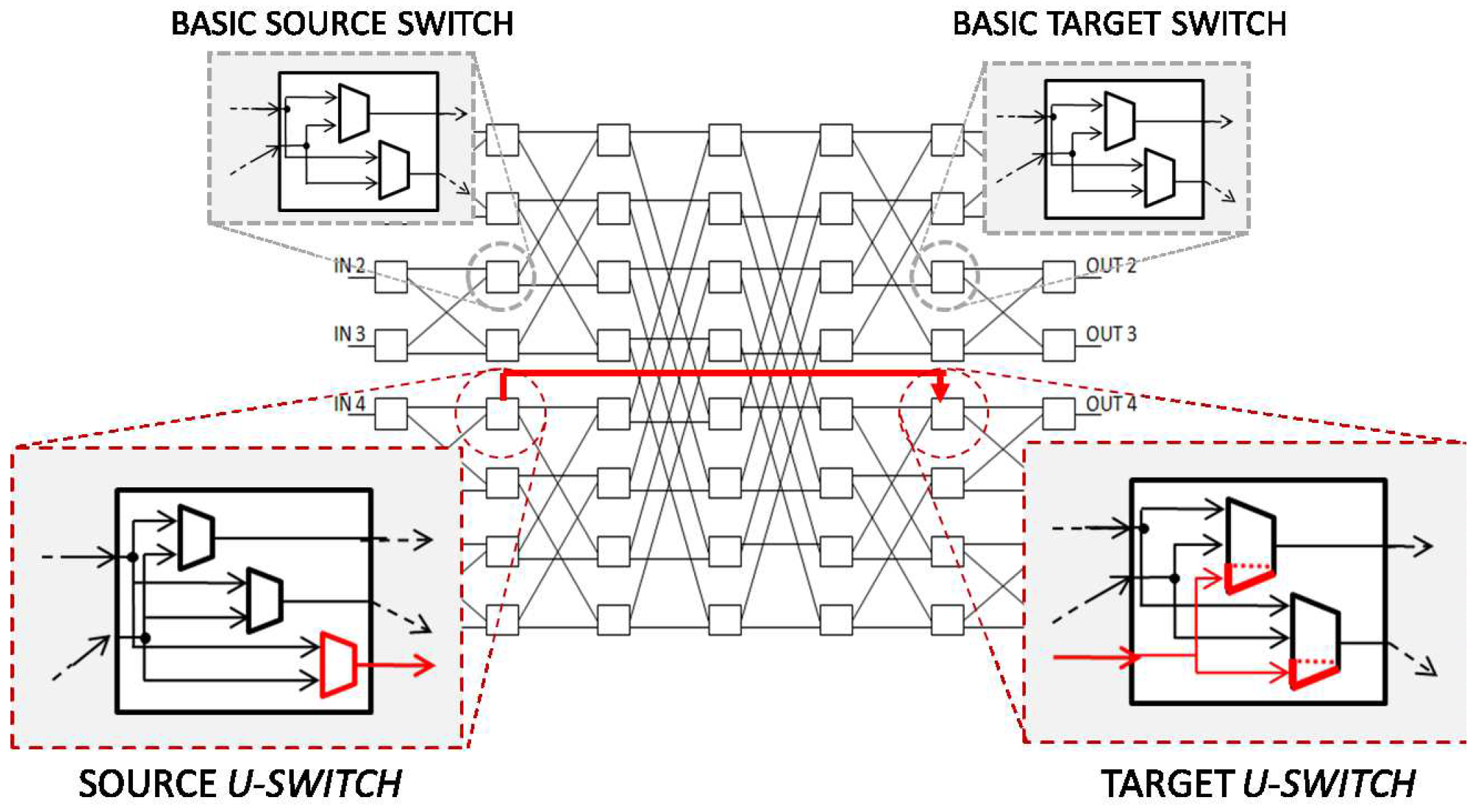
Adding extra stages to obtain RNB features makes latency a critical point of the network. For that reason, and to overcome the fact that butterfly topologies cannot exploit traffic locality, an alternative hierarchy-aware folded version of the MSSN was devised. Leveraging on its symmetry properties, the flat (Figure 3a) MSSN can hence be folded at the central stage, creating a bypassed architecture [4] in which, thanks to the addition of a set of dedicated U-turn connections to the basic switches, an intrinsic hierarchical structure can be exploited. As shown in Figure 4, the application of U-turn connections to each stage of a folded MSSN allows groups () of U-switches at stage S to be created, which define butterfly-based sub-networks: this potentially allows the upper levels of the hierarchy to be bypassed, thus exploiting local connectivity without any impact on congestion. As an example, in Figure 4 the sub-network obtained grouping the upper switches allows any connections between I/O from 0 to 3 to be performed bypassing the upper level of switches.
The bypassed version of the MSSN inherits the RNB properties from the flat topology. In fact, as shown in the unfolded view of Figure 5, U-turn bypasses allows non-adjacent stages to be bridged thanks to the addition of dedicated logic, extra pins, and independent configuration bits to each basic SE. We obtain more routing paths and available connections, allowing each bypassed sub-network to keep the same RNB characteristics as flat architecture. With reference to Figure 4, each switch at stage S, for S from 1 to , is composed by source and target U-switches, while the switch in the central stage ( is a simple basic switch.
Regardingto the area penalties, these are balanced by performance improvements. Benefits will accrue when the area increase becomes an investment by computational density growth. This aspect will be analyzed in Section 7.
4.3. Radix-k MSSN
The previous analyses is extended to networks with switch elements in the MID stages. Parameter k is the radix of the network. MSSN described in Figure 3 is hence a radix-2 flat MSSN (with ), while Figure 6 shows a radix-4 flat network, with . With reference to Figure 2b, this network is equivalent to a MSSN with two planes, each made of a Banyan network with extra stages, in addition to input/output switches.
Focusing on butterfly-based MSSNs, and generalizing condition (2) for a generic radix-k, the number of stages becomes:
Adding x extra stages as before, namely , the total number of network stages for horizontal cascading strategy is:
which takes the form of (5) when .
Hwang and Lin [35] generalized the condition (3) for a generic radix-k for unicast connectivity, demonstrating that the number of vertical planes p necessary in order that the networks have the RNB feature is:
Therefore, taking , (10) becomes always satisfied for any value of both number N of I/Os and radix-k. IN, OUT, and MID stages are all composed of SEs, with . Since , in a radix-2 MSSN, while in a radix-4 MSSN. Regarding the multicast connectivity, we have carried out numerous routing tests without finding any critical situation for the routing scheme.
5. MSSN Programming Strategy
In order to speed up architectural exploration and validation, we implemented a software tool capable to provide both the register-transfer-level (RTL) MSSN description and the configuration bitstream according to the user application. The target architecture is described specifying MSSN parameters, such as the number N of I/Os and number of stages. In addition, it allows one to specify the switch elements (SE) used (i.e., radix-k) at each stage and the intra-stage connectivity patterns (e.g., the two butterfly topologies in Figure 3a,b and stages with bypass enhancements as in Figure 5).
Following [4], the MSSN routing engine is an iteration-based path-finding algorithm. The nets are sorted and routed sequentially taking into account the available resources (i.e., the SE). Net sorting is done based on criticality, which tracks the historical difficulty to route each net and is updated after each routing iteration according to the success/fail current attempt. Iterations stop when all the nets are routed successfully. The algorithm splits multi-fanout nets into independently routed single-fanout nets that can share routing resources.
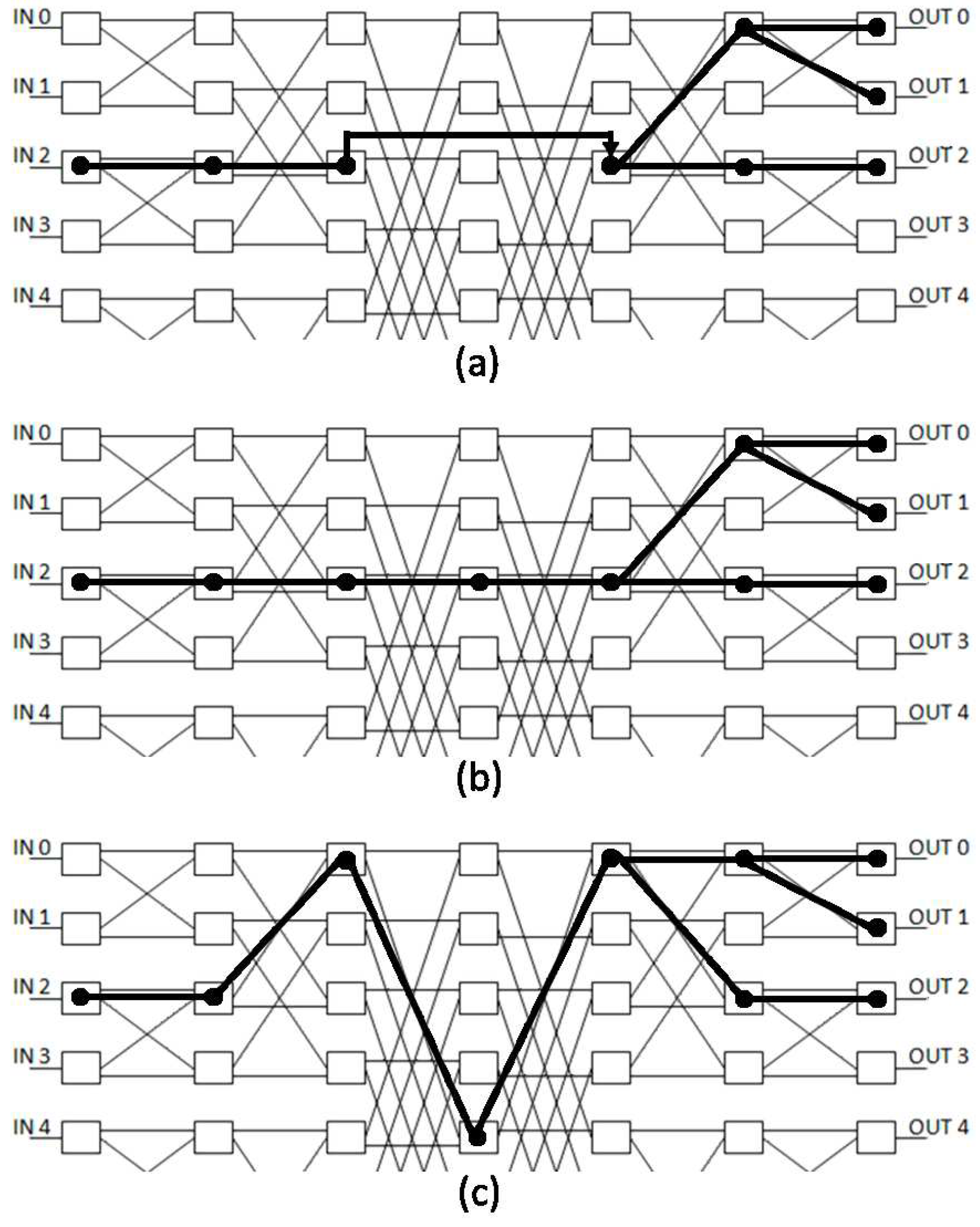
Path-finding strategy is based on Dijkstra’s algorithm for weighted graphs [36]. The SEs represent the graph nodes connected by weighted edges, which correspond to the wires used to connect MSSN stages. The algorithm tries to find the cheapest path among all available ones, whereas the cost of a path is the sum of the traversed wire’s weights. Weights are a fundamental part of the architecture description: they drive routing policy toward preferred solutions and impact convergence speed. We found that assigning lower weights to bypasses and straight paths (zeroing weight for sharable resources) allows to achieve an as-straight-as-possible policy which resulted the best solution for both convergence and bypass utilization (Figure 7). Thanks to this approach, we found that, on networks with dimensions up to 4K I/Os, the number of iterations needed to solve the routing lies in average between 5 and 10.
The utilization of a butterfly-based MSSN as interconnection infrastructure also changes the distance metric used on the placement algorithms [4]. In fact, trying to minimize the net delays, traditional placement algorithms for FPGA or ASIC (Application-Specific Integrated Circuit) have the goal to minimize the distances among cells, whereas the distance is measured in a 2D space (be it the L1 Manhattan distance or L2 distance), tightly coupled with the Elmore delay associated to the connection. On a hierarchical butterfly MSSN, i.e., with bypass enhancement, the delay is associated to the number of stages to be crossed to connect two points. As visible in Figure 4, the distance among primary I/Os is not linear, but follow some steps which also depend on the radix of the network. With reference to Figure 4, only switches up to must be crossed to connect to , while all the switches up to are crossed when the required connection is between and . This aspect is known as the boundary-radix problem [10] and is a limiting factor for the use of such networks in large FPGA. In small size eFPGAs, as the ones we are tackling, this problem is mitigated by replacing 2D distance metric with a wire length defined as, for generic radix-k:
where (between 1 and ) is the minimum stage S subtending all the points to be connected, as discussed in [4], and is due to the bypass connection. This way, the placement tool tries to limit to the number of switches crossed to achieve a full exploitation of the hierarchical topology. A different approach has been followed by [10] where the boundary-radix problem has been addressed in hardware by isomorphic transformations, which makes the MSSN less regular.
6. Flat MSSN Performance versus Radix-k
In this section, we show the implementation results of two flat MSSNs featuring radix-2 and radix-4, respectively. The purpose of this analysis is to demonstrate that the synthesizability allows one to exploit a significant design space to find the best radix for a given class of applications. The test-case we consider is a I/Os flat MSSN. According to Equation (5), the radix-2 network features stages, including:
- one IN and one OUT stage with switches;
- MID stages with switches.
For radix-4 MSSN, the number of stages, defined by (8) with , is , and the RNB property is obtained with half the switches per stage () compared to the radix-2, but with a more complex structure (Figure 6). The MSSN hence features:
- one IN stage composed of switches;
- MID stages with switches;
- one OUT stage composed of switches.
For both architectures a set of physical synthesis have been performed using Synopsys Design Compiler Graphical [37] targeting STMicroelectronics CMOS 65 nm LP 1.2 V standard cell libraries. Adopted physical synthesis flow was industrially qualified by the foundry to be well correlated with implementation and silicon. This notwithstanding, some place-and-routes were carried out to further verify feasibility of the approach (especially against routing congestion) on few relevant cases, resulting in a good correlation in line with Electronic Design Automation (EDA) vendor figures. Since target technology makes available standard cells with 3 different voltage thresholds (Low, Standard, and High Voltage Threshold—LVT, SVT, HVT), a couple of different standard cells mixes were analysed: a SVT-only for area-optimization and a mix of HVT+SVT+LVT to target high-speed optimization (HVT are included for leakage optimization on configuration structures). Time-to-fly between one input and one output is the critical path of the network and thus is constrained by the target implementation period, whereas all the configuration pins of the MSSN switches are quasi-static paths and were considered false-paths.
Post-synthesis results are provided in Table 1 for both MSSNs, targeting either area or speed optimization. The resulting design space is significant, with a range of ≃ for frequency and a range of ≃ in terms of area for both radix-2 and radix-4 MSSNs. It shows that the radix-4 solution radically increases area in min-area implementations (), while in the max-speed case the area penalty is lower (). This is due to both the synthesis optimizations criteria adopted and the fact that in the min-area case we considered two iso-frequency (200 MHz) implementations, while in the max-speed case we reached different frequencies (400 vs. 480 MHz).
Each MSSN architecture was also implemented changing the target frequency between the min-area and the max-speed targets. The obtained results are reported for iso-frequency values in Figure 8a, showing similar trends for both architectures: radix-2 MSSN provides better area performance for any frequency value. With the purpose of comparing the two architectures in terms of frequency performance, Figure 8b reports the implementation results for iso-area values: again in this case, radix-2 MSSN guarantees better performance, with a wider gap for low area values.
This area increase can be justified with a “handcrafted” analysis of the logic complexity of both architectures in terms of number of equivalent MUX2:1. Flat radix-2 MSSN requires stages as defined in (5); observing Figure 3a and Figure 5, it can be noted that input stage does not require any MUX, output stage is composed by a single MUX2:1 and middle stages by two MUX2:1. By considering switches per stage, the total number of equivalent MUX2:1 (MUXeqradix-2) can therefore be expressed as:
For , radix-2 MSSN features therefore ≃ 40K equivalent MUX2:1. On the other hand, in a radix-4 MSSN the middle switches (Figure 6) can be seen to be made of 4 MUX4:1, each corresponding to 3 MUX2:1, the 4 × 2 switches in output stage require 2 MUX4:1 while the input stage still does not require any MUX. From (8) and considering switches per stage, the total number of equivalent MUX2:1 (MUXeq) can be therefore expressed as:
For the total number of equivalent MUX2:1 proves to be ≃58K, a increase with respect to the radix-2 solution. Despite of that, a class of applications where radix-4 structure provides better performance will be observed in Section 7.3. In addition, this overhead can be mitigated leveraging on optimized standard cells libraries capable to reduce the intrinsic MUX4:1/MUX2:1 area-ratio thanks pass-transistor exploitation.
7. Flat versus Hierarchical MSSN Performance
This section evaluates hierarchical MSSNs featuring U-turn bypasses, focusing on finding the best tradeoff between area overhead, due to the additional logic in the U-switches, and the improvements in frequency performances. This will help compare the radix-2 and radix-4 MSSN more effectively, like the flat MSSN versions.
The test case we consider is again a I/Os MSSN, radix-2 and radix-4, with U-turn bypasses applied to realize either a fully-bypassed network (fully), with bypasses at each MSSN stage, or a half-bypassed one (half), with bypasses only at odd stages. STM CMOS 65 nm LP is still the target technology, considering two different mixes of standard cells: SVT-only for area optimization and full mix with H+S+LVT for high-speed.
Post synthesis results for all three versions (flat, half, and fully) are shown in Table 2 for radix-2 and Table 3 for radix-4 MSSN, with two different implementations optimized by area or by speed: for both, the area overhead introduced by the bypass enhancement is straightforward. As for the flat version, the half- and the fully-bypassed architectures were implemented varying the target implementation frequency according to the values in Table 2. As previously defined, implementation frequency is the time-to-fly between MSSN input and output; the delay due to crossing switches of all MSSN stages is therefore considered.
7.1. MSSN Delay Model and Validation
In [4] we developed a post-synthesis application-aware analysis to evaluate the performances improvement thanks to the introduction of bypassed switching elements. Different benchmarks were mapped (through the custom eFPGA CAD flow) on both the flat architecture and the fully-bypassed radix-2 version of the eFPGA. This showed that introducing a bypassed MSSN allows increasing the working frequency by a factor, frequency gain, from ≃ to ≃ depending on the target application and therefore on the capability to exploit the bypass feature. Starting from these data, in [4] we then proposed a computational analysis that takes into account eFPGA critical path length (i.e., the longest combinational path composed of both LB and MSSN delays) based on the ability of bypass enhancement to guarantee frequency gains in a range between and with respect to the flat version. In that analysis one of the key assumptions is that the internal MSSN stages, both in the flat and in the bypassed version, feature homogeneous delays, so that the delay associated with a single stage in an MSSN with stages is approximated as:
where is the delay of the whole MSSN (i.e., the implementation period in Table 2 and Table 3). As an example, for the radix-2 fully-bypassed implementation, is ns for max speed and ns for min area.
Hence, according to (12), in the evaluation of the eFPGA critical path the effective MSSN IN2OUT delays is considered to be proportional to the stage (S in 1 to ) in which the U-turn connection was exploited (e.g., the group of switches in Figure 4), so that:
where the factor is due to the fact that the network has to be crossed back and forth (corresponding to crossing the source and target switches in Figure 5) and the take into consideration input and output stage. The case corresponds to non-exploitation of the bypass: all MSSN stages are crossed and the IN2OUT delay reduces to the implementation period .
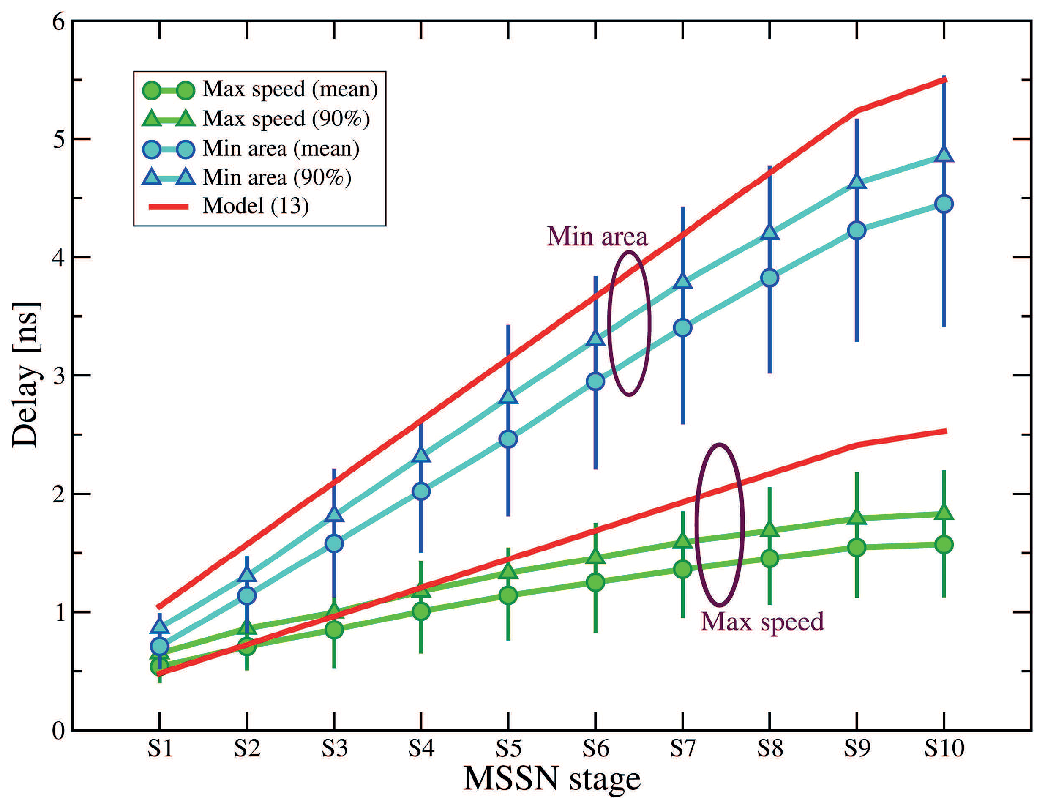
In order to validate the model based on (12) and (13), and adopted in [4], in Figure 9 we show the difference between piecewise linear model (13) and a set of real (post synthesis) input-to-output delays for the fully-bypassed radix-2 implementation. Such delays were obtained, both in the max speed and min area implementations of the fully-bypassed I/Os radix-2 MSSN of Table 2, by forcing the timing analysis tool to exploit the bypass connections at different MSSN stages (, with , in the horizontal axis in Figure 9). corresponds to non-bypass exploitation. Since for each input/output pair the I/Os MSSN provides 1024 possible paths, the results are represented as clusters of points. Solid lines (one for the max speed and one for the min area case) represents the piecewise linear model obtained from (13).
It can be observed that piecewise linear model (13) represents a sort of “worst-case” compared to the mean values, lines with circular markers, or to the ninetieth percentile values, triangular markers, of real delays. The only cases where the model under-estimate the network delay are those which consider a bypass exploitation at the lowest levels (, and in Figure 9) of the MSSN hierarchy in the max speed implementation. However, when considered in the evaluation of a completely programmable device, such a gap in the approximations would hardly affect computation of the critical path, since dominated by the contribution of the computational logic block (LB) delay.
Similar results were obtained when taking into account a radix-4 architecture and data from Table 3, where the stage delay is larger than that in a radix-2 architecture, due to the greater complexity of radix-4 switch elements (Figure 6).
The previous results allow us to validate model (13) and to apply it to the comparison between different MSSN architecture options, as will be done in Section 7.2 and Section 7.3.
7.2. MSSN Effective Frequency Versus Bypass Exploitation
To evaluate the area/speed tradeoff of different MSSN architectures, in this paragraph we use model (13) to perform a computational density analysis considering interconnect structures with the same area but different number of stages with U-turn connections. Whereas for the flat MSSN (Section 6) we considered the implementation frequency as a figure of merit, since the network delay corresponds to the MSSN full latency, in the bypassed MSSN the actual working frequency has to be taken into account. A bypassed MSSN (Figure 4) provides shorter paths for logically near I/O pins, and thus the working frequency depends on the locality of the connections required by the applications. As explained in Section 5, locality is tackled by optimized routing strategy, which targets the best bypass utilization. As an example, Figure 7a,b show two paths exploiting (a) and non-exploiting (b) a bypass enhancement, respectively. According to (13), the effective delay of path (a) where the stage S in which the bypass is exploited is would be lower than the one in (b) where thanks to bypassing switch .
Figure 10 [5] reports the effective frequency of a flat MSSN together with what is achievable by a bypass-enhanced MSSN, assuming four ranges of frequency gain corresponding to different levels of bypass exploitation ( non-exploitation of the bypasses, , , ).
As reported in Table 2, the minimum area necessary to realize a flat version of MSSN is mm, mm for half-bypassed and mm for fully-bypassed. The post-synthesis results in Table 2 are referred to the full-latency of the MSSN ( bypass exploitation). Hence, targeting small area devices (< mm) the flat MSSN is the unique solution among those listed. The half-bypassed architecture (Figure 10a) proves advantageous for area > mm, since it allows to achieve higher frequencies even if the frequency gain is around , while reaching time-to-fly frequency values beyond 700 MHz when the area is not a tight constraint.
The same idea is applied to the fully-bypassed MSSN (Figure 10b), where frequency >450 MHz can be reached with greater area budgets, while for area <0.8 mm the flat MSSN can provide higher speeds even with frequency gain >. Compared to the half-bypassed solution, and below 650 MHz, fully-bypassed architecture enables lower frequencies, owing to increased design density. On the other hand, a fully-bypassed MSSN provides a higher probability of bypass exploitation. With a passing reference to this aspect, in this analysis we have decided not to take into account architectures with a lower application of bypasses (e.g., realizing a quarter-bypassed MSSN), since with a lower probability of bypass exploitation the frequency gain values might no longer be applicable.
Applying the same analysis to a radix-4 MSSN, we achieved similar results: advantages provided by introducing U-turn bypasses, either in half stages or in the full network, only become evident targeting high frequencies, with the drawback of additional area requirements.
7.3. Comparison between Different Radices for Hierarchical MSSN
The validated in Section 7.1 is then used to perform a comparison in terms of area/speed tradeoffs for different radix in hierarchical MSSN. In Section 6 we showed that, in a flat architecture, an MSSN featuring radix-2 switches is able to guarantee better area and implementation frequency performances than its equivalent radix-4 version. Given this comparison, and since in the previous sections we proved that both the half-bypassed and the fully-bypassed architectures can improve effective working frequency with respect to flat architecture, an analysis of the tradeoffs between area occupancy and the opportunities presented by U-turn bypasses in both radix-2 and radix-4 MSSN is performed in this paragraph.
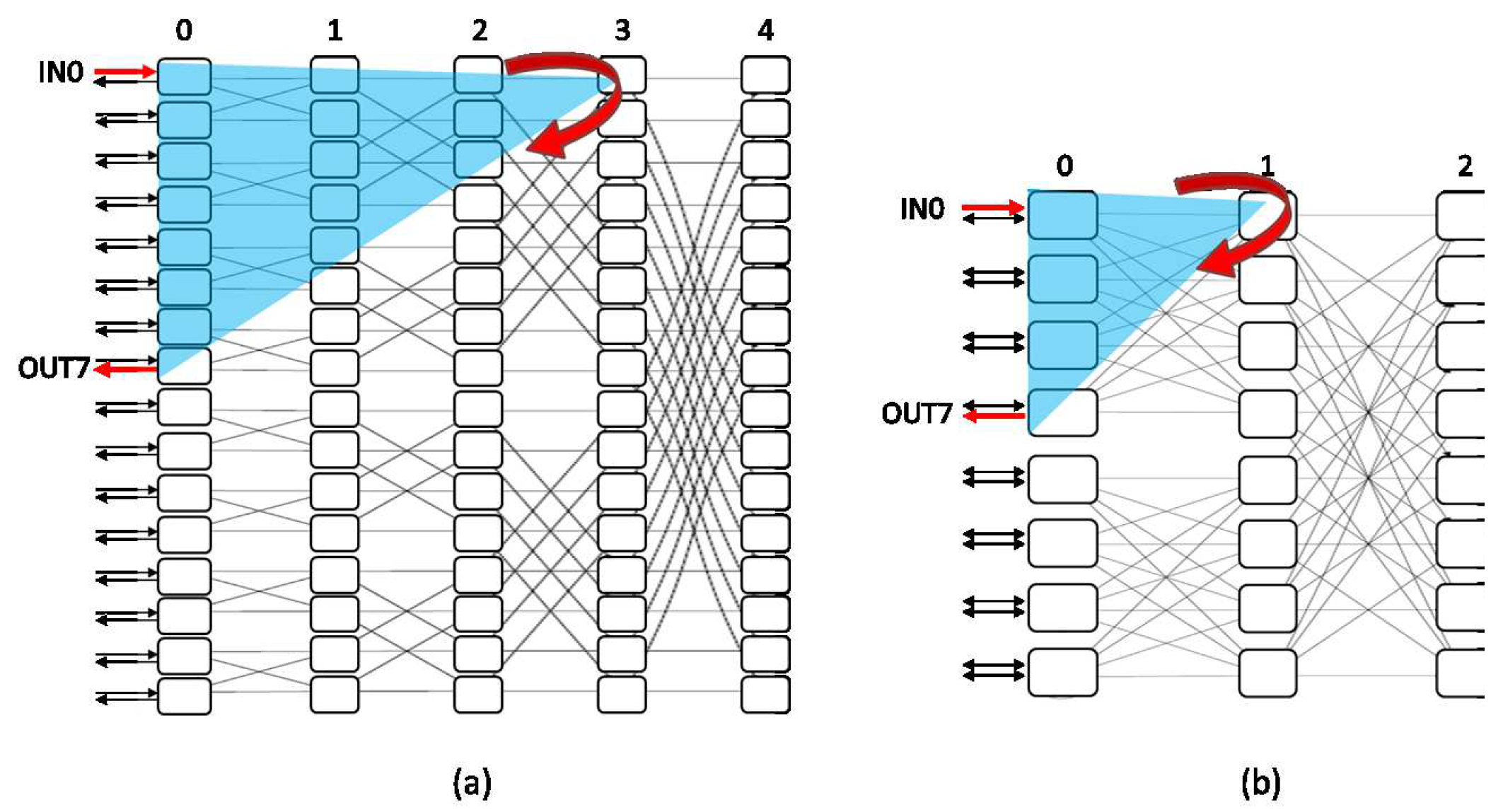
Variation of MSSN radix implies different exploitation of the locality of the connections. In fact, the number of stages to cross in order to connect two MSSN I/Os proves to be different. By way of example, as shown in Figure 11 [5], in a I/Os radix-2 fully-bypassed MSSN the minimum common stage, S in (13), connecting IN0 to OUT7 is stage , while in the corresponding radix-4 topology only stage has to be crossed. In the radix-2 architecture the number of points (inputs and outputs) subtended from a cone of height S is:
while in the radix-4 architecture:
where the 2 factor is due to the fact that each IN and OUT stage is connected to two I/Os (Figure 6 and Figure 11b). Extending to a generic radix-k, the number of points turns out to be:
for S from 1 to . In the previous equation (>0) is a factor that takes into account the number of inlets (outlets) connected to each IN/OUT stage . From the preceding definitions of Section 4.3:
To understand Equaiton (16), let us re-write it as:
For a generic stage S, the number of points subtended from a cone of the previous stage is:
Therefore, at the “current” stage S, the points subtended are those of the previous stage multiplied by k if S isn’t the central stage of the network (). In the case of stage , the different planes (Figure 2) are merged in the central stage (Figure 4) hence, the total number of points is the sum of the points of the previous stage of each p plane (i.e., multiplied by p). Thanks to (18), (17) can be written as:
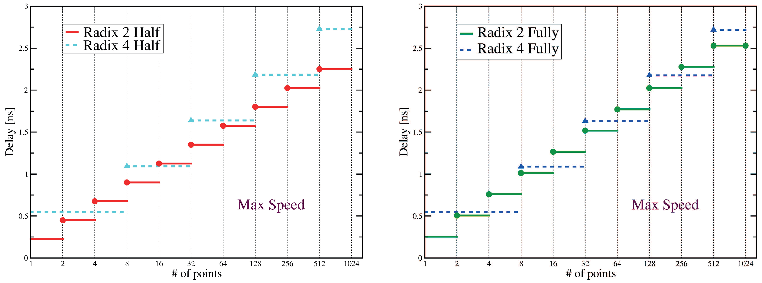
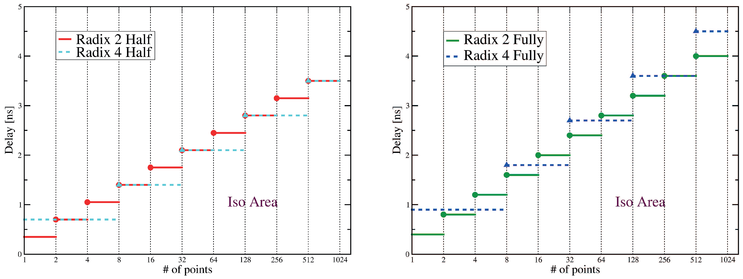
which corresponds to (16). The half-bypassed and fully-bypassed version of a I/Os MSSN, both radix-2 and radix-4, were compared. Assuming that the CAD tool discussed in Section 5 places MSSN I/Os minimizing their distance forcing , we analyzed the number of stages, hence the delay, required to connect two I/Os placed at different distances, according to wire-length definition (11). A set of implementations, including both max speed and iso-area, were considered: for each, the stage delay was calculated according to (12), and the computed with (13).
Figure 12 and Figure 13 report the results for different distances between two MSSN I/Os that are to be connected. The results obtained (HVT+SVT+LVT implementations) show that there is not a unique solution for the MSSN architecture. Design constraints and the capability of the CAD to exploit bypass affect the MSSN architectural choice. In the max speed implementations (Figure 12) the radix-4 MSSN (dashed lines) proves advantageous, i.e., less delay in the average, only when the distance between points is not too large. On the contrary, for iso-area implementations (Figure 13), radix-4 MSSN (dashed lines) allows lower interconnect delay for any distance between points in the half-bypassed structure and in the fully-bypassed version is still advantageous in the average for small distances between I/Os, i.e., when application fields exploit local connectivity.
The analysis can be extended to larger values of radix-k. It is worth noting that the area occupation of switch element increases with while the granularity of bypass exploitation decreases, hence reducing the probability of performance gain.
8. Conclusions
We presented an analysis of a class of MSSN suitable for the implementation of routing in ePLD, i.e., soft-core IPs with size in the order of 1 KLUTs, showing full-static multicast connectivity capabilities and the possibility to be synthesized. We described also a parametric programming tool which allows many architectural variations to be applied without affecting the overall routability properties. The implemented programming strategy allows to achieve a straight-as-possible policy in order to minimize the boundary-radix problem, which could affect the performance of hierarchical log-networks.
The MSSNs were implemented in STM CMOS 65 nm technology: the results reveal a significant design space in terms of area/speed tradeoffs, resulting in a range of ≃ for frequency and a range of ≃ in terms of area. Furthermore, the introduction of U-turn bypasses enabled the design space to be enlarged, providing a frequency performance improvement (up to ), at the expense of increased area occupancy.
The parametric MSSN structure was also exploited varying the radix: a comparison between a radix-2 and a radix-4 was then performed, for both bypassed and non-bypassed architectures. The results show that the area-frequency tradeoff is in favor of the radix-2 architecture for low area budgets, while the radix-4 solution is able to provide a better exploitation of the connection locality.
Author Contributions
Conceptualization, F.R., M.C., C.M., E.F.S. and R.C.; Methodology, F.R., M.C., C.M., E.F.S. and R.C.; Software, M.C., F.R. and C.M.; Validation, F.R. and C.M.; Data curation, F.R. and M.C.; Writing—original draft preparation, F.R. and M.C.; Writing—review and editing, C.M., E.F.S. and R.C.; Visualization, F.R.; Supervision, C.M., E.F.S. and R.C.
Funding
This work was supported in part by R2POWER300 project that has received funding from the ECSEL JU Joint Undertaking Call 2014-2 under grant agreement n 653933.
Conflicts of Interest
The authors declare no conflict of interest.
References
- Baschirotto, A.; Castello, R.; Campi, F.; Cesura, G.; Toma, M.; Guerrieri, R.; Lodi, R.; Lavagno, L.; Malcovati, P. Baseband analog front-end and digital back-end for reconfigurable multi-standard terminals. IEEE Circuits Syst. Mag. 2006, 6, 8–28. [Google Scholar] [CrossRef] [Green Version]
- Ho, M.H.; Ai, Y.Q.; Chau, T.C.P.; Yuen, S.C.L.; Choy, C.S.; Leong, P.H.; Pun, K.P. Architecture and design flow for a highly efficient structured ASIC. IEEE Trans. Very Large Scale Integr. Syst. 2013, 21, 424–433. [Google Scholar] [CrossRef]
- Rossi, D.; Mucci, C.; Pizzotti, M.; Perugini, L.; Canegallo, R.; Guerrieri, R. Multicore signal processing platform with heterogeneous configurable hardware accelerators. IEEE Trans. Very Large Scale Integr. Syst. 2014, 22, 1990–2003. [Google Scholar] [CrossRef]
- Cuppini, M.; Mucci, C.; Scarselli, E.F. Soft-Core Embedded–FPGA Based on Multistage Switching Networks: A Quantitative Analysis. IEEE Trans. Very Large Scale Integr. Syst. 2015, 23, 3043–3052. [Google Scholar] [CrossRef]
- Cuppini, M. Methodologies for Synthesizable Programmable Devices Based on Multi-Stage Switching Networks. Ph.D. Thesis, University of Bologna, Bologna, Italy, May 2015. Available online: http://amsdottorato.unibo.it/7013/1/Cuppini_Matteo_Tesi.pdf (accessed on 28 February 2019).
- Kim, J.; Anderson, J. Synthesizable Standard Cell FPGA Fabrics Targetable by the Verilog-to-Routing CAD Flow. ACM Trans. Reconfigurable Technol. Syst. (TRETS) 2017, 10. [Google Scholar] [CrossRef]
- DeHon, A. The density advantage of Configurable Computing. Computer 2000, 33, 41–49. [Google Scholar] [CrossRef]
- Cuppini, M.; Scarselli, E.F.; Mucci, C.; Canegallo, R. Soft-core eFPGA for Smart Power applications. In Proceedings of the 2014 International Symposium on System-on-Chip (SoC), Tampere, Finland, 28–29 October 2014. [Google Scholar]
- Brant, A.; Lemieux, G.G.F. ZUMA: An open FPGA overlay architecture. In Proceedings of the 2012 IEEE 20th International Symposium on Field-Programmable Custom Computing Machines, Toronto, ON, Canada, 29 April–1 May 2012; pp. 93–96. [Google Scholar]
- Yuan, F.; Wang, C.; Yu, T.H.; Markovic, D. A multi–granularity FPGA with hierarchical interconnects for efficient and flexible mobile computing. IEEE J. Solid-State Circuits 2015, 50, 137–149. [Google Scholar] [CrossRef]
- Kuon, I.; Tessier, R.; Rose, J. Fpga Architecture: Survey and Challenges; Foundations and Trends in Electronic Design Automation; Now Publishers Inc.: Delft, The Netherlands, 2008; Volume 2. [Google Scholar]
- Rose, J.; Gamal, A.E.; Sangiovanni-Vincentelli, A. Architecture of field-programmable gate arrays. Proc. IEEE 1993, 81, 1013–1029. [Google Scholar] [CrossRef]
- Tsu, W.; Macy, K.; Joshi, A.; Huang, R.; Walker, N.; Tung, T.; Rowhani, O.; George, V.; Wawrzynek, J.; DeHon, A. HSRA: High-speed, hierarchical synchronous reconfigurable array. In Proceedings of the 1999 ACM/SIGDA Seventh International Symposium on Field Programmable Gate Arrays, Monterey, CA, USA, 21–23 February 1999; pp. 125–134. [Google Scholar]
- Amerson, R.; Carter, R.J.; Culbertson, W.B.; Kuekes, P.; Snider, G. Teramac-configurable custom computing. In Proceedings of the IEEE Symposium on FPGAs for Custom Computing Machines, Napa Valley, CA, USA, 19–21 April 1995; pp. 32–38. [Google Scholar]
- Amerson, R.; Carter, R.; Culbertson, W.; Kuekes, P.; Snider, G.; Albertson, L. Plasma: An FPGA for Million Gate Systems. In Proceedings of the Fourth International ACM Symposium on Field-Programmable Gate Arrays, Napa Valley, CA, USA, 11–13 February 1996; pp. 10–16. [Google Scholar]
- Reblewski, F.; Lepape, O. Reconfigurable Integrated Circuit with a Scalable Architecture. U.S. Patent 6594810, 4 October 2001. [Google Scholar]
- Wong, D. Interconnection Network for a Field Programmable Gate Array. U.S. Patent 6693456, 3 August 2001. [Google Scholar]
- Wang, C.; Yuan, F.L.; Chen, H.; Markovic, D. A 1.1 GOPS/mW FPGA chip with hierarchical interconnect fabric. In Proceedings of the 2011 Symposium on VLSI Circuits–Digest of Technical Papers, Honolulu, HI, USA, 15–17 June 2011; pp. 136–137. [Google Scholar]
- Wang, C.; Markovic, D. Network Architectures for Boundary-Less Hierarchical Interconnects. Patent WIPO 2014/144832 A1, 14 March 2014. [Google Scholar]
- DeHon, A.; Rubin, R. Design of FPGA interconnect for multilevel metallization. IEEE Trans. Very Large Scale Integr. (VLSI) Syst. 2004, 12, 1038–1050. [Google Scholar] [CrossRef] [Green Version]
- Dally, W.J.; Towles, B.P. Principles and Practices of Interconnection Networks; Elsevier: Amsterdam, The Netherlands, 2004. [Google Scholar]
- Clos, C. A Study of Non–Blocking Switching Networks. Bell Syst. Tech. J. 1953, 32, 406–424. [Google Scholar] [CrossRef]
- Yang, Y.; Wang, J. Nonblocking k–fold multicast networks. IEEE Trans. Parallel Distrib. Syst. 2003, 14, 131–141. [Google Scholar] [CrossRef]
- Yang, Y.; Wang, J. On blocking probability of multicast networks. IEEE Trans. Commun. 1998, 46, 957–968. [Google Scholar] [CrossRef]
- Agrawal, D.P. Graph theoretical analysis and design of multistage interconnection networks. IEEE Trans. Comput. 1983, C-32, 637–648. [Google Scholar] [CrossRef]
- Wu, C.; Feng, T. On a class of multistage interconnection networks. IEEE Trans. Comput. 1980, C-29, 694–702. [Google Scholar]
- Pattavina, A. Switching Theory: Architectures and Performances in Broadband ATM Networks; Wiley: Hoboken, NJ, USA, 1998. [Google Scholar]
- Lea, C. Multi–log2N networks and their applications in high-speed electronic and photonic switching systems. IEEE Trans. Commun. 1990, 38, 1740–1749. [Google Scholar] [CrossRef]
- Benes, V.E. Mathematical Theory of Connecting Networks and Telephone Traffic; Academic Press: New York, NY, USA, 1965; Volume 17. [Google Scholar]
- Benes, V.E. Optimal rearrangeable multistage connecting networks. Bell Syst. Tech. J. 1964, 43, 1641–1656. [Google Scholar] [CrossRef]
- Jiang, X.; Pattavina, A.; Horiguchi, S. Rearrangeable f-cast multi-log2N networks. IEEE Trans. Commun. 2008, 56, 1929–1938. [Google Scholar] [CrossRef]
- Lea, C.; Shyy, D. Tradeoff of horizontal decomposition versus vertical stacking in rearrangeable nonblocking networks. IEEE Trans. Commun. 1991, 39, 899–904. [Google Scholar] [CrossRef]
- Tscha, Y.; Lee, K.H. Nonblocking conditions for multi-log2N multiconnection networks. In Global Telecommunications Conference, GLOBECOM’92, Communication for Global Users; IEEE: Piscataway, NJ, USA, 1992; Volume 3, pp. 1600–1604. [Google Scholar]
- Collier, M. A systematic analysis of equivalence in multistage networks. J. Lightw. Technol. 2002, 20, 1664–1672. [Google Scholar] [CrossRef] [Green Version]
- Hwang, F.K.; Lin, W.D. Necessary and sufficient conditions for rearrangeable logd(N, m, p). IEEE Trans. Commun. 2005, 53, 2020–2023. [Google Scholar] [CrossRef]
- Dijkstra, E.W. A note on two problems in connexion with graphs. Numer. Math. 1959, 1, 269–271. [Google Scholar] [CrossRef] [Green Version]
- Synopsys. Design Compiler Tool in Graphical Mode; Synopsys: Mountain View, CA, USA, 2018. [Google Scholar]
Figure 1.
An (with N = 16) Banyan multistage switching network (MSSN) featuring butterfly topology.

Figure 2.
Example of construction of Multi- networks: with horizontal cascading (a) and vertical stacking (b) technique.
Figure 2.
Example of construction of Multi- networks: with horizontal cascading (a) and vertical stacking (b) technique.

Figure 3.
An (with ) flat version of the proposed MSSN: original architecture (a) and rearrangeably non-blocking (RNB)-proof unicast topologically equivalent version (b).
Figure 3.
An (with ) flat version of the proposed MSSN: original architecture (a) and rearrangeably non-blocking (RNB)-proof unicast topologically equivalent version (b).

Figure 4.
Folded bypassed MSSN enhanced with U-turn bypasses.


Figure 6.
An example of radix-4 flat MSSN.

Figure 7.
Three different multi-fanout paths connecting to , , and in order of cost: with bypass enhancement (a), with the as-straight-as-possible policy (b), and using diagonal wires (c).
Figure 7.
Three different multi-fanout paths connecting to , , and in order of cost: with bypass enhancement (a), with the as-straight-as-possible policy (b), and using diagonal wires (c).

Figure 8.
I/Os Flat MSSN radix-2 (B2) versus radix-4 (B4): iso-frequency (a) and iso-area (b) post-synthesis results.
Figure 8.
I/Os Flat MSSN radix-2 (B2) versus radix-4 (B4): iso-frequency (a) and iso-area (b) post-synthesis results.

Figure 9.
I/Os radix-2 MSSN in-to-out delays (with bypass exploitation at different stages) compared to model (13) varying the MSSN stage S in which the U-turn connection is exploited.
Figure 9.
I/Os radix-2 MSSN in-to-out delays (with bypass exploitation at different stages) compared to model (13) varying the MSSN stage S in which the U-turn connection is exploited.

Figure 10.
I/Os radix-2 MSSN effective frequency versus area for different frequency gain thanks to bypass exploitation: flat vs. half-bypassed (a) and fully-bypassed (b).
Figure 10.
I/Os radix-2 MSSN effective frequency versus area for different frequency gain thanks to bypass exploitation: flat vs. half-bypassed (a) and fully-bypassed (b).

Figure 11.
Example of fully-bypassed MSSN connectivity with I/Os: radix-2 (a) and radix-4 (b).

Figure 12.
Max-speed implementations: delay vs. topological distance between two I/Os for a fully-bypassed and half-bypassed MSSN.
Figure 12.
Max-speed implementations: delay vs. topological distance between two I/Os for a fully-bypassed and half-bypassed MSSN.

Figure 13.
Iso-area implementations: delay vs. topological distance between two I/Os for a fully-bypassed and half-bypassed MSSN.
Figure 13.
Iso-area implementations: delay vs. topological distance between two I/Os for a fully-bypassed and half-bypassed MSSN.


Table 1.
CMOS 65 nm flat multistage switching networks (MSSN) post-synthesis summary: radix-2 and radix-4.
Table 1.
CMOS 65 nm flat multistage switching networks (MSSN) post-synthesis summary: radix-2 and radix-4.
| Implementation Results | Radix-2 | Radix-4 | ||
|---|---|---|---|---|
| Min Area | Max Speed | Min Area | Max Speed | |
| Area [mm2] | 0.20 | 0.80 | 0.27 | 0.89 |
| Impl. Freq. [MHz] | 200 | 480 | 200 | 400 |
| Cells Mix | SVT | H+S+LVT | SVT | H+S+LVT |
Table 2.
CMOS 65 nm radix-2 MSSN post-synthesis results.
| Implementation Results | Min Area | Max Speed | ||||
|---|---|---|---|---|---|---|
| Flat | Half | Fully | Flat | Half | Fully | |
| Area [mm2] | 0.20 | 0.34 | 0.40 | 0.80 | 0.89 | 1.01 |
| Impl. Freq. [MHz] | 200 | 200 | 180 | 480 | 445 | 395 |
| Cells Mix | SVT | H+S+LVT | ||||
Table 3.
CMOS 65 nm radix-4 MSSN post-synthesis results.
| Implementation Results | Min Area | Max Speed | ||||
|---|---|---|---|---|---|---|
| Flat | Half | Fully | Flat | Half | Fully | |
| Area [mm2] | 0.27 | 0.33 | 0.49 | 0.89 | 0.90 | 1.1 |
| Impl. Freq. [MHz] | 200 | 200 | 200 | 400 | 365 | 367 |
| Cells Mix | SVT | H+S+LVT | ||||
© 2019 by the authors. Licensee MDPI, Basel, Switzerland. This article is an open access article distributed under the terms and conditions of the Creative Commons Attribution (CC BY) license (http://creativecommons.org/licenses/by/4.0/).
Share and Cite
MDPI and ACS Style
Renzini, F.; Cuppini, M.; Mucci, C.; Franchi Scarselli, E.; Canegallo, R. Quantitative Analysis of Multistage Switching Networks for Embedded Programmable Devices. Electronics 2019, 8, 272. https://doi.org/10.3390/electronics8030272
AMA Style
Renzini F, Cuppini M, Mucci C, Franchi Scarselli E, Canegallo R. Quantitative Analysis of Multistage Switching Networks for Embedded Programmable Devices. Electronics. 2019; 8(3):272. https://doi.org/10.3390/electronics8030272
Chicago/Turabian StyleRenzini, Francesco, Matteo Cuppini, Claudio Mucci, Eleonora Franchi Scarselli, and Roberto Canegallo. 2019. "Quantitative Analysis of Multistage Switching Networks for Embedded Programmable Devices" Electronics 8, no. 3: 272. https://doi.org/10.3390/electronics8030272
Note that from the first issue of 2016, this journal uses article numbers instead of page numbers. See further details here.