Low-Cost Portable Reader for Frequency Domain Chipless Tags: Architecture and Experimental Results on Depolarizing Tags


 ,
,
Abstract
:1. Introduction
2. Reader Architecture
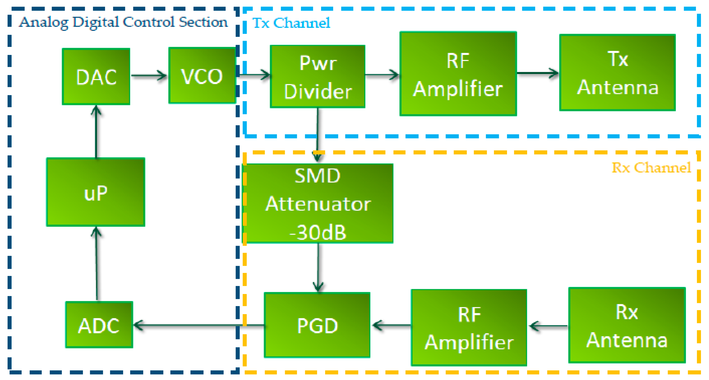
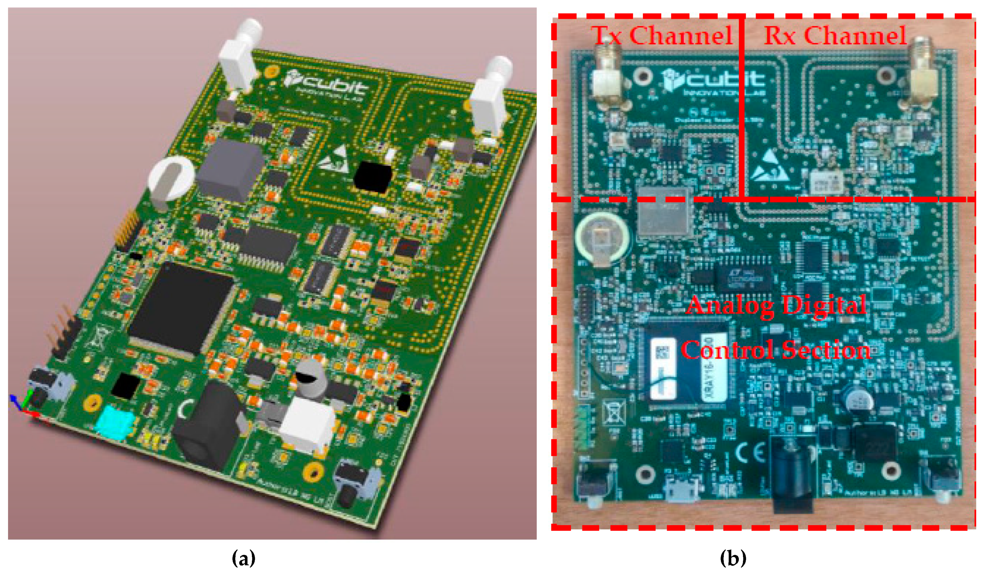
2.1. Hardware Architecture
- Analog/Digital control section: $45 for 1 K pcs;
- RF Tx Channel: $35 for 1 K pcs;
- RF Rx Channel: $40 for 1 K pcs;
2.1.1. Analog/Digital Control Section
- 1x Microprocessor: A 32-bit general purpose MCU (Microcontroller unit) with 96 MHz clock frequency, Floating Point Unit (FPU), and a large amount of integrated flash memory. The core architecture also supports DSP (Digital Signal Processing) functions with a 32-bit multiplier, divider, and multiply-accumulator with integrated 2 MB of flash memory, 128 KB of RAM, and 32 KB of data flash memory;
- 1x Digital to Analog Converter (DAC): A 12-bit multiplying digital-to-analog converter with parallel input. It has high accuracy, stability over temperature and supply variations, and lower sensitivity to output amplifier offset. This very versatile DAC is useful for two-quadrant and four-quadrant multiplying, programmable gain and filtering, and single-supply noninverting voltage output operations;
- 1x Voltage Controlled Oscillator: A VCO with a frequency range from 2020 MHz to 2490 MHz, output power of 7.2 dBm, tuning sensitivity of 30 MHz/V, tuning voltage of 0.25 V to 16 V, pulling of 2.5 MHz;
- 1x Analog to Digital Converter: A 12-bit high-speed, low-power, successive approximation ADC. The device operates from a single 2.7 V to 5.25 V power supply, and it has a throughput rate of up to 1.5 MSPS. (Mega Samples per Second) It contains a low-noise, wide-bandwidth track-and-hold amplifier that can handle input frequencies in excess of 1 MHz.
2.1.2. RF Tx Channel
- 1x Power Divider (RoHS compliant): An SMD power splitter that offers a wide bandwidth from 1750 MHz to 3000 MHz. In addition, it has good isolation up to 20 dB and good output VSWR (Voltage Standing Wave Ratio);
- 1x RF Amplifier (RoHS compliant): An advanced ultra-flat gain amplifier (up to 15 dB, P1 dB 19 dBm) fabricated using E-PHEMT technology which offers an extremely high dynamic range over a broad frequency range and with a low noise figure. In addition, it has good input and output return loss over a broad frequency range without the need of external matching components;
- 1x Tx Antenna (see paragraph reader antenna).
2.1.3. RF Rx Channel
- 1x Rx Antenna (see paragraph reader antenna);
- 1x RF Amplifier (RoHS compliant), similar to the Tx channel;
- 1x Phase/Gain Detector (PGD), a fully integrated system for measuring gain/loss and phasing in numerous receiving, transmitting, and instrumentation applications. The ac-coupled input signals can range from −60 dBm to 0 dBm in a 50 Ω system, from low frequencies up to 2.7 GHz. The outputs provide an accurate measurement of either gain and of phase. Both subsystems have an output bandwidth of 30 MHz;
- 1x SMD Attenuator with a miniature package of 3 × 3 mm, which has an attenuation of 30 dB up to 3000 MHz and excellent VSWR of 1:15:1.
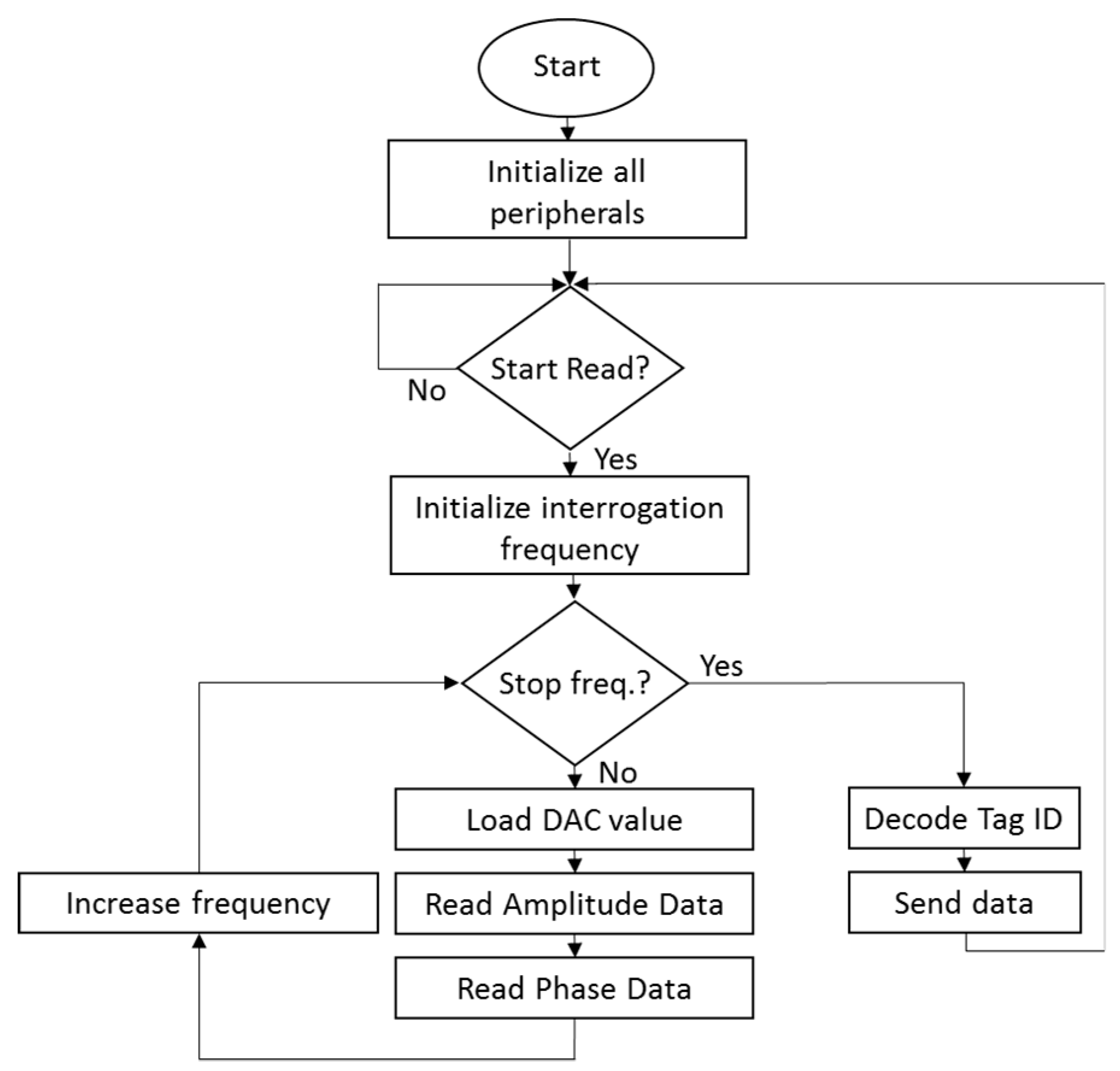
2.2. Firmware
3. Cross-Polar Tags
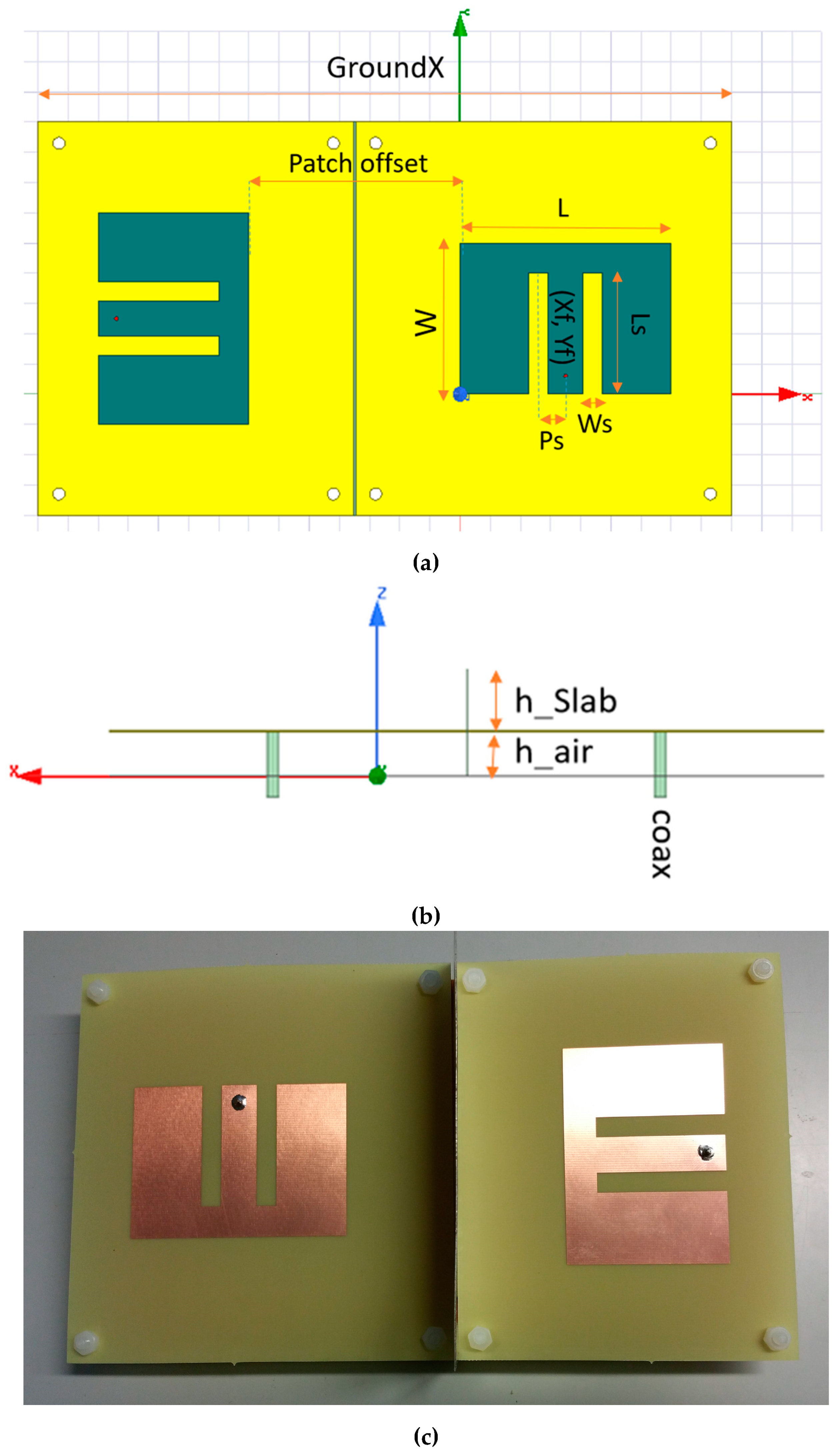
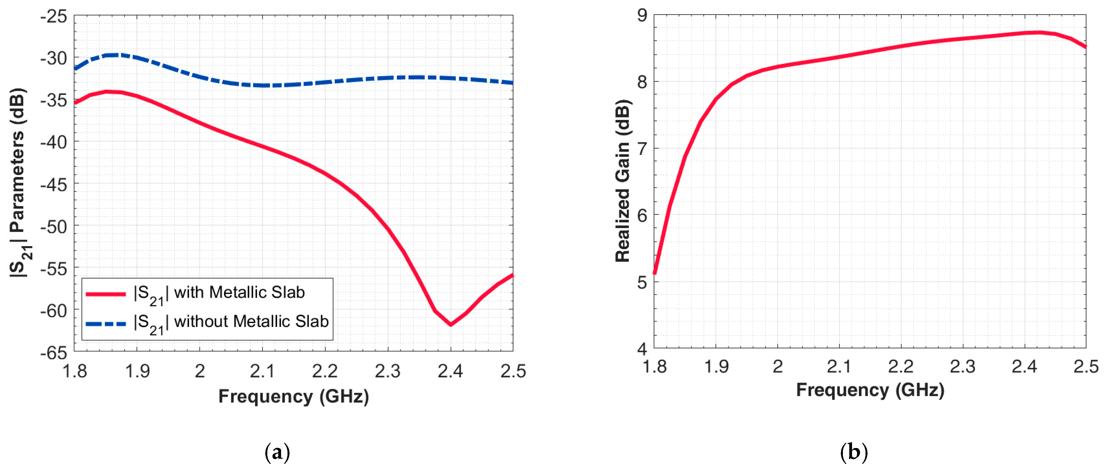
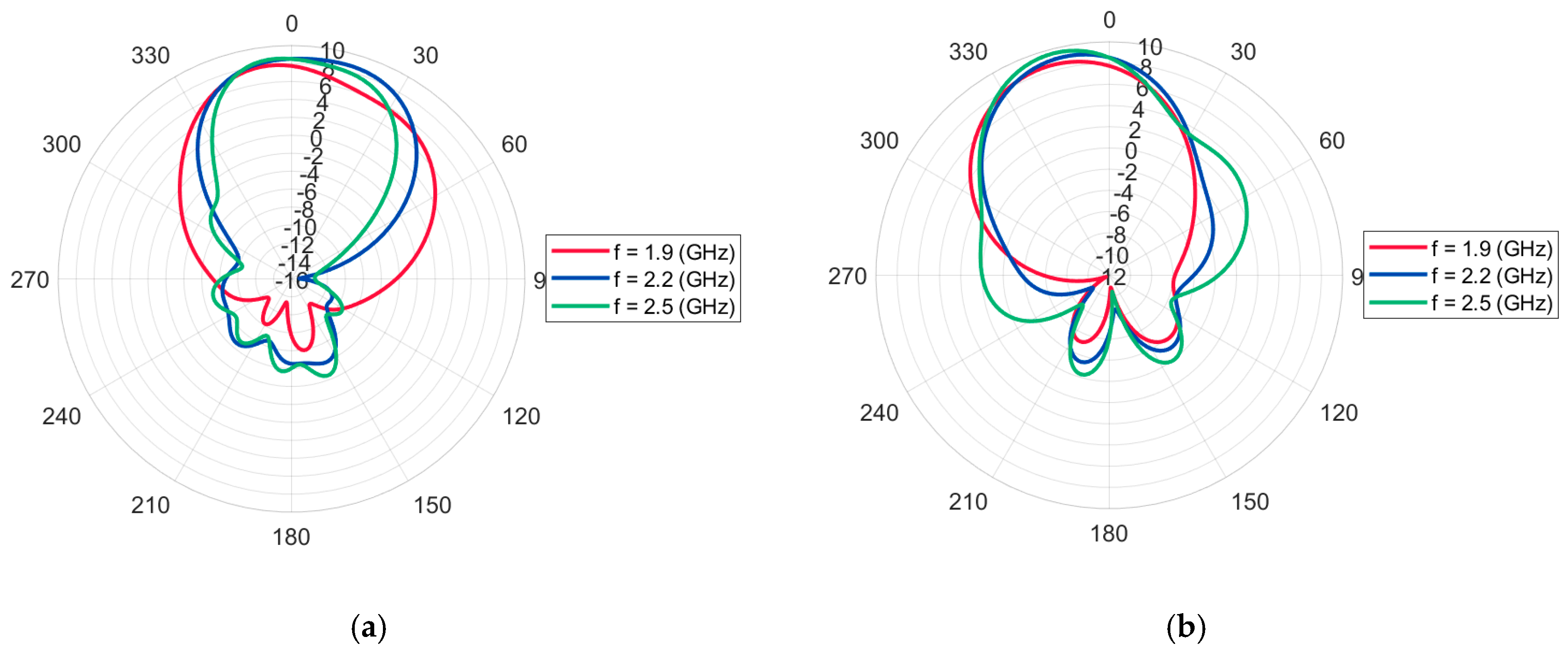
4. Reader Antennas
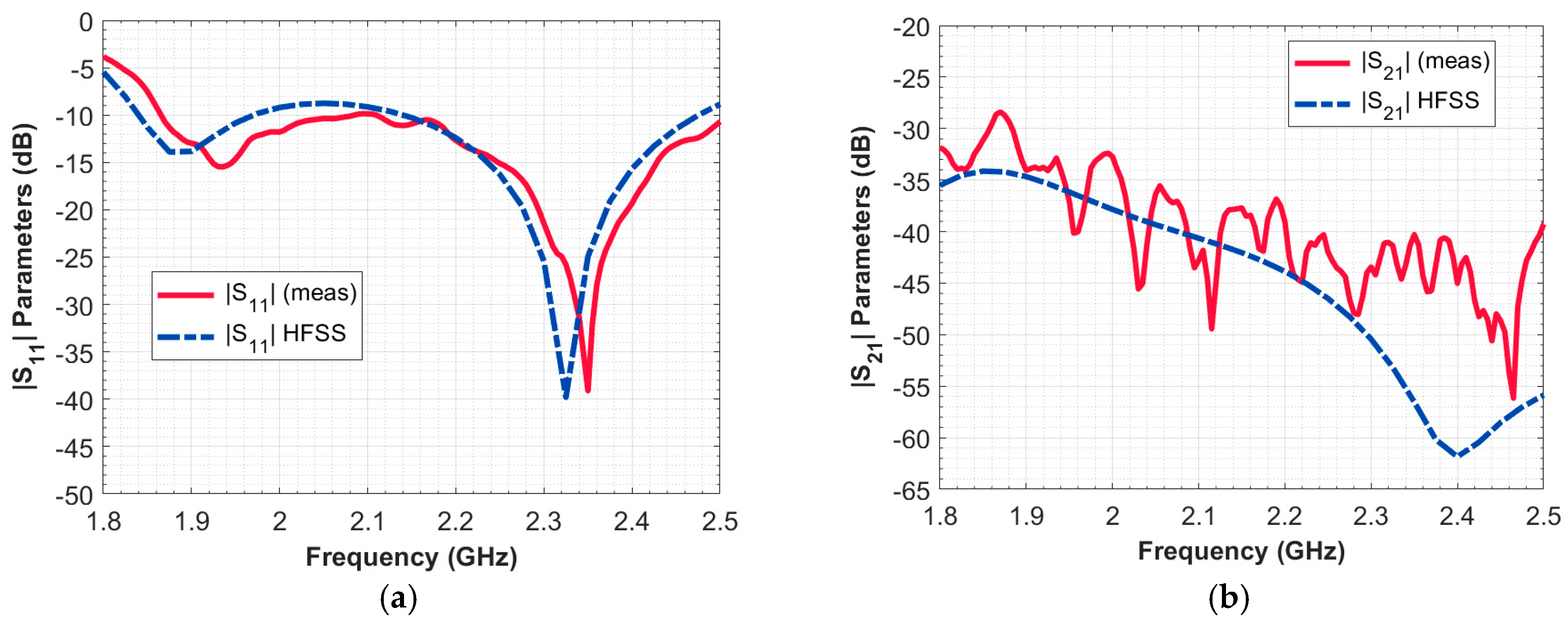
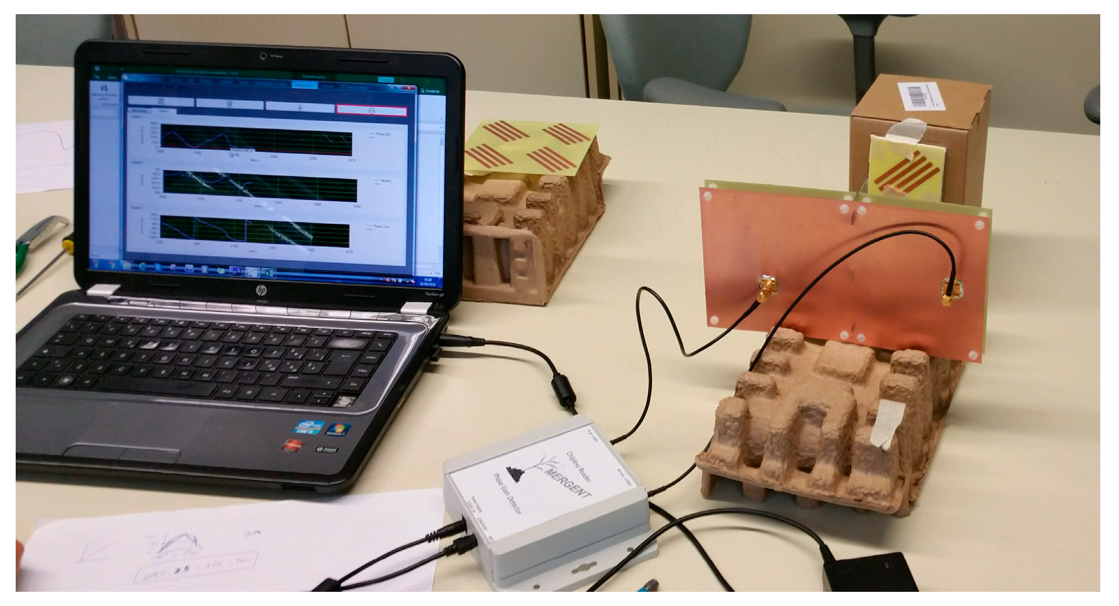
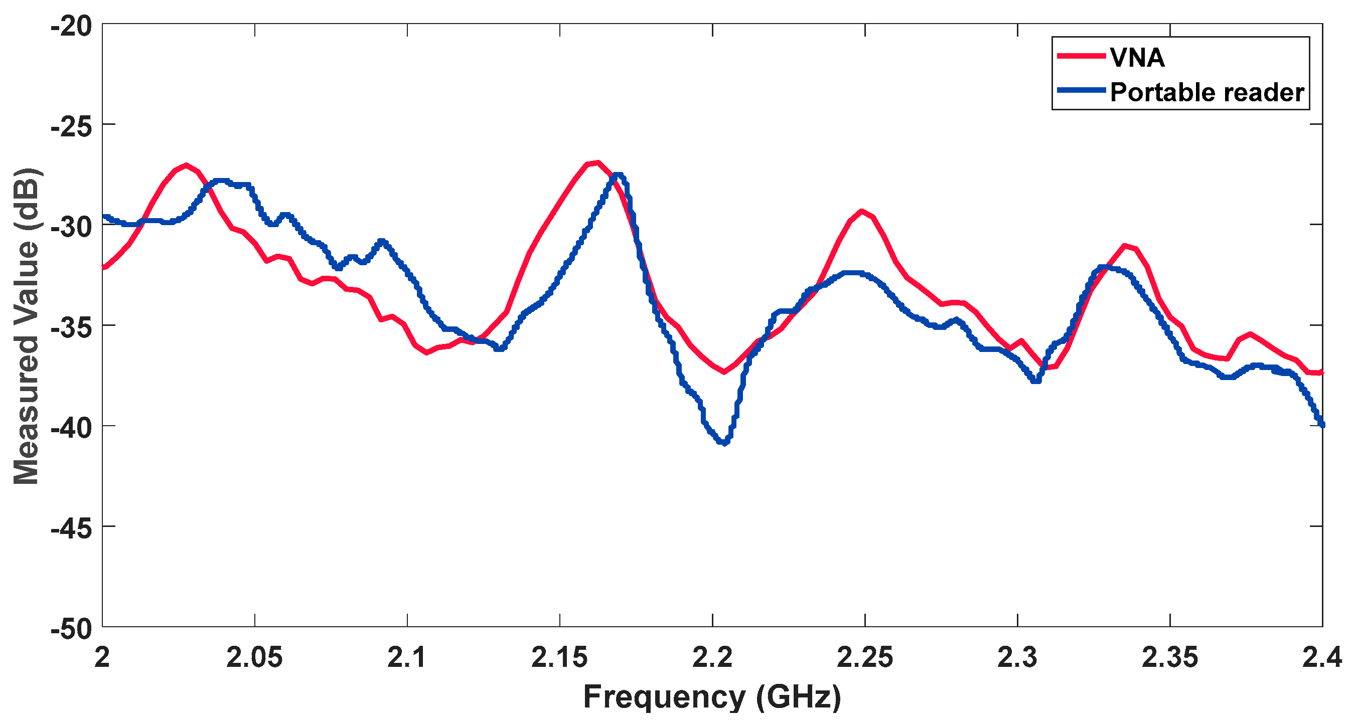
5. Experiments
6. Discussion
7. Conclusions
Author Contributions
Funding
Conflicts of Interest
References
- Ramos, A.; Girbau, D.; Lazaro, A.; Villarino, R. Wireless Concrete Mixture Composition Sensor Based on Time-Coded UWB RFID. IEEE Microw. Wirel. Compon. Lett. 2015, 25, 681–683. [Google Scholar]
- Costa, F.; Genovesi, S.; Monorchio, A. A Chipless RFID Based on Multiresonant High-Impedance Surfaces. IEEE Trans. Microw. Theory Tech. 2013, 61, 146–153. [Google Scholar] [CrossRef]
- Vena, A.; Perret, E.; Tedjini, S. Chipless RFID Tag Using Hybrid Coding Technique. IEEE Trans. Microw. Theory Tech. 2011, 59, 3356–3364. [Google Scholar] [CrossRef]
- Preradovic, S.; Karmakar, N.C. Design of short range chipless RFID reader prototype. In Proceedings of the 2009 International Conference on Intelligent Sensors, Sensor Networks and Information Processing (ISSNIP), Melbourne, Australia, 7–10 December 2009; pp. 307–312. [Google Scholar]
- Vithalkar, A. Chipless RFID reader. Bachelor’s Thesis, Delhi University, New Delhi, India, 18 April 2018. [Google Scholar]
- Preradovic, S.; Karmakar, N.C. Multiresonator based chipless RFID tag and dedicated RFID reader. In Proceedings of the 2010 IEEE MTT-S International Microwave Symposium, Anaheim, CA, USA, 23–28 May 2010; pp. 1520–1523. [Google Scholar]
- Koswatta, R.V.; Karmakar, N.C. A Novel Reader Architecture Based on UWB Chirp Signal Interrogation for Multiresonator-Based Chipless RFID Tag Reading. IEEE Trans. Microw. Theory Tech. 2012, 60, 2925–2933. [Google Scholar] [CrossRef]
- Karmakar, N.C.; Koswatta, R.; Kalansuriya, P.; E-Azim, R. Chipless RFID Reader Architecture; Artech House: Norwood, MA, USA, 2013; ISBN 978-1-60807-561-4. [Google Scholar]
- Garbati, M.; Siragusa, R.; Perret, E.; Halopé, C. Low cost low sampling noise UWB Chipless RFID reader. In Proceedings of the 2015 IEEE MTT-S International Microwave Symposium, Phoenix, AZ, USA, 17–22 May 2015; pp. 1–4. [Google Scholar]
- Garbati, M.; Perret, E.; Siragusa, R. Chipless RFID Reader Design for Ultra-Wideband Technology: Design, Realization and Characterization; Elsevier: Oxford, UK, 2018; ISBN 978-0-08-102761-5. [Google Scholar]
- Lázaro, A.; Villarino, R.; Costa, F.; Genovesi, S.; Gentile, A.; Buoncristiani, L.; Girbau, D. Chipless Dielectric Constant Sensor for Structural Health Testing. IEEE Sens. J. 2018, 18, 5576–5585. [Google Scholar] [CrossRef]
- XeThru Shop. Single-Chip Radar Sensor with Sub-mm Resolution—XeThru. Available online: https://shop.xethru.com/ (accessed on 4 December 2018).
- UWB Radar|UWB Sensor|2D ISAR|3D ISAR|RCS Systems|UWB Antenna|Delay Line. Available online: http://www.geozondas.com/main_page.php?pusl=5 (accessed on 4 December 2018).
- Borgese, M.; Costa, F.; Genovesi, S.; Monorchio, A.; Manara, G. Multi-frequency polarizarition converter with enhanced angular robustness. In Proceedings of the 2016 IEEE International Symposium on Antennas and Propagation (APSURSI), Fajardo, Puerto Rico, 26 June–1 July 2016; pp. 669–670. [Google Scholar]
- Borgese, M.; Costa, F.; Genovesi, S.; Monorchio, A.; Manara, G. Optimal Design of Miniaturized Reflecting Metasurfaces for Ultra—Wideband and Angularly Stable Polarization Conversion. Sci. Rep. 2018, 8, 7651. [Google Scholar] [CrossRef]
- Mittra, R.; Chan, C.H.; Cwik, T. Techniques for analyzing frequency selective surfaces—A review. Proc. IEEE 1988, 76, 1593–1615. [Google Scholar] [CrossRef]
- Costa, F.; Gentile, A.; Genovesi, S.; Buoncristiani, L.; Lazaro, A.; Villarino, R.; Girbau, D. A Depolarizing Chipless RF Label for Dielectric Permittivity Sensing. IEEE Microw. Wirel. Compon. Lett. 2018, 28, 371–373. [Google Scholar] [CrossRef]
- Yang, F.; Zhang, X.-X.; Ye, X.; Rahmat-Samii, Y. Wide-band E-shaped patch antennas for wireless communications. IEEE Trans. Antennas Propag. 2001, 49, 1094–1100. [Google Scholar] [CrossRef]
- Blischak, A.T.; Manteghi, M. Embedded Singularity Chipless RFID Tags. IEEE Trans. Antennas Propag. 2011, 59, 3961–3968. [Google Scholar] [CrossRef]
- Garbati, M.; Siragusa, R.; Perret, E.; Halopé, C. Impact of an IR-UWB Reading Approach on Chipless RFID Tag. IEEE Microw. Wirel. Compon. Lett. 2017, 27, 678–680. [Google Scholar] [CrossRef]
- Buchanan, N.B.; Fusco, V. Single VCO chipless RFID near-field reader. Electron. Lett. 2016, 52, 1958–1960. [Google Scholar] [CrossRef] [Green Version]


| Analog/Digital Control Section | RF Tx Channel | RF Rx Channel |
|---|---|---|
| Microprocessor R5F5631ECDFB: $8.2 | Pwr Divider BP2U1+: $1.05 | Antenna: $15 |
| DAC LTC7545ABSW#PBF: $4.3 | RF Amp PGA-105+: $1.55 | RF Amp PGA-105+: $1.55 |
| VCO ROS-2490C+: $17.3 | Antenna: $15 | PG Detector AD8302ARUZ: $12.5 |
| ADC AD7472ARUZ: $9.9 | Passive components + other: $7.7 | Passive components + other: $2.95 |
| PCB + Passive components + other: $2.3 | Assembling + functional test: 9.7$ | Assembling + functional test: 8$ |
| Assembling + functional test: $3 | ||
| Total: $45 | Total: $35 | Total: $40 |
| Total costs for 1 K pcs: $120 | ||
| Reference | [7] | [19] | [20] | [21] | This work |
| Operating bandwidth | 4–8 GHz | 50–20.5 GHz | 3.1–10.6GHz | 2.4–3.4 GHz | 2–2.5 GHz |
| Reader system | PCB circuit | VNA-based | PCB circuit | VCO, oscilloscope, ramp generator | PCB circuit |
| Cost | <$650 | high | <2.5 Keuro (antenna not included) | medium | $120 (antenna included) |
| # of reference measurements | No need of a reference measurements | Reference measurements required | No need of a reference measurements | Reference measurements required | No need of a reference measurements |
© 2019 by the authors. Licensee MDPI, Basel, Switzerland. This article is an open access article distributed under the terms and conditions of the Creative Commons Attribution (CC BY) license (http://creativecommons.org/licenses/by/4.0/).
Share and Cite
Boggioni, L.; Monti, L.; Terranova, S.; Costa, F.; Genovesi, S.; Manara, G. Low-Cost Portable Reader for Frequency Domain Chipless Tags: Architecture and Experimental Results on Depolarizing Tags. Electronics 2019, 8, 35. https://doi.org/10.3390/electronics8010035
Boggioni L, Monti L, Terranova S, Costa F, Genovesi S, Manara G. Low-Cost Portable Reader for Frequency Domain Chipless Tags: Architecture and Experimental Results on Depolarizing Tags. Electronics. 2019; 8(1):35. https://doi.org/10.3390/electronics8010035
Chicago/Turabian StyleBoggioni, Luca, Lorenzo Monti, Sergio Terranova, Filippo Costa, Simone Genovesi, and Giuliano Manara. 2019. "Low-Cost Portable Reader for Frequency Domain Chipless Tags: Architecture and Experimental Results on Depolarizing Tags" Electronics 8, no. 1: 35. https://doi.org/10.3390/electronics8010035