Article

Resistive High-Voltage Probe with Frequency Compensation by Planar Compensation Electrode Integrated in Printed Circuit Board Design

Department of Sensors and Measurement Technology, Institute of Electrical Engineering and Measurement Technology, Leibniz Universität Hannover, Appelstr. 9A, 30167 Hannover, Germany
*
Author to whom correspondence should be addressed.
Electronics 2022, 11(21), 3446; https://doi.org/10.3390/electronics11213446
Submission received: 26 September 2022 / Revised: 14 October 2022 / Accepted: 18 October 2022 / Published: 25 October 2022
(This article belongs to the Topic High Voltage Engineering)

Abstract

:
Resistive voltage dividers tend to have a highly non-linear transfer function as parasitic and stray capacitances exert an increasing influence with increasing frequency. The non-linear transfer function depends on the topology and resistors used and consists of a low-pass filter with an additional high-pass component in the GHz range. Due to the non-linear transfer function the measured signal differs from the original input signal. Here, we present an improved resistive voltage divider with additional compensation capacities to extend the linear bandwidth. With this new concept, the linear bandwidth is improved from 115 kHz to 88 MHz, while maintaining a DC input impedance of 10 MΩ. For high-voltage insulation and easy manufacturing, surface mounted resistors on a printed circuit board with a compensation electrode on the adjacent side are used. The performance of this resistive voltage divider is demonstrated by measuring a series of high-voltage pulses with an amplitude of 2.5 kVpeak-peak. The measured pulse rise time is about 16 ns, corresponding to an average slew-rate of 150 V/ns. Finally, the developed resistive voltage divider is successfully used to measure fast high-voltage transients required for advanced ion mobility spectrometers with integrated collision induced fragmentation.

1. Introduction

The precise measurement of high voltages occurs in different applications, such as monitoring of ultra-high-voltage transmission lines [1], spectrometry, electron mass determination [2], pulse width modulation for electrical motors [3], or pulsed gas lasers [4] (pp. 491–493).
There are several approaches for measuring fast high-voltage pulses, as they occur in sensor applications, especially in ion mobility spectrometry (IMS) and mass spectrometry. In IMS [5,6,7], [8] (pp. 125–127), [9], for example, measurements of fast high-voltage pulses are essential for the functionality, e.g., the separation of the ions in a field asymmetric time of flight ion mobility spectrometer (FAT-IMS) [7,10]. For these measurements, a constant transfer function over a wide frequency range is important for precisely measuring the waveforms occurring in the aforementioned applications, consisting of a DC voltage in the kilovolt (kV) range with superimposed fast high voltage pulses [3,11].
With commercially available direct current (DC) high-voltage probes, voltages measurements are only possible to a limited extent, since the maximum measurable voltage decreases rapidly with increasing frequency [12,13]. The strong frequency dependence of the input impedance usually leads to high input currents in the high-voltage probe and, therefore, has a significant effect on the measured signal. This results in an imprecise measurement of the signal waveform, and is due to the parallel parasitic capacitance of the input impedance. Compared to DC high-voltage probes, alternating current (AC) high-voltage probes are better suited for measuring fast high-voltage pulses since the transmission behavior corresponds to a high-pass filter. However, high-pass filters severely limit their use for DC voltages. In applications with high DC and superimposed high AC voltages, AC high-voltage probes are not usable for measuring both, AC and DC.
One approach to precisely measure high voltages (>1 kV AC or >1.5 kV DC according to DIN EN 50110-1 [14]) is shown by Bauer et al. [2]. However, large input capacitance leads to a low cut-off frequency, so that this attempt is not feasible to measure high-voltage transients. A design that is suitable for recording fast high-voltage transients is shown by He et al. [15], using a copper sulphate solution in an acrylic glass cylinder as the resistive material. This design achieves rise-times between 10 ns to 15 ns. The major issue of this design is the reduced input impedance of approximately 2.1 kΩ, which is too low for measuring superimposed high DC voltages.
Another approach for a compensated voltage divider, to achieve a linear transfer function is shown by Grubmüller et al. [3]. They also used a design based on a printed circuit board (PCB) with discrete surface mounted devices (SMD) capacitors for frequency compensation. This enables an easy to assemble setup by using commercially available SMD components. However, the limiting factor of this approach is the low breakdown voltage of 1 kV and the limited bandwidth to 10 MHz [3].
The final approach worth mentioning here to acquire a signal containing DC and AC components is described by Shi et al. [11]. Their approach uses a ceramic tube resistor with a conductive layer vaporized on the outside and a compensation electrode made of a specially shaped metallic torso inserted inside. Through this inserted cone, an almost constant transmission behavior of the resistive voltage divider is achievable up to a frequency of 1 GHz [11]. The maximum achieved input impedance is 250 kΩ, which is still too low for high DC voltages and leads to an excessive distortion of the measurement signal, due to the high input current. In addition, the size of the resistive voltage divider developed by Shi et al. is too large (approximately Ø 50 mm × 200 mm [11]) for many applications and precise fabrication of the torso is expensive compared to our single PCB approach.
Here, we present our analog compensation approach for resistive voltage divider, based on the design by Shi et al. [7], but with a much larger input impedance and significantly reduced probe size. The compensation approach is based on a special PCB design and can be implemented by only using SMD components, thus allowing a simple and low-cost setup [16] (p. 154). The frequency compensation is realized with PCB traces forming a compensation electrode that is located on adjacent PCB layers. To achieve optimal compensation for a linear transmission response of the resistive voltage divider from DC over a wide frequency range, various geometric shapes of the compensation electrode were designed and investigated with field simulations in the Dassault Systémes (Vélizy-Villacoublay, France) CST Studio Suite 2021® Microwaves and RF solver and measurements. The characteristics of the developed resistive voltage divider were determined and further optimized by the use of a vector network analyzer (VNA).
Then, the transmission response of the optimized resistive voltage divider was characterized by the transient response of a high-voltage step. For this purpose, a commercially available high-voltage push-pull stage Behlke Power Electronics GmbH (Kronberg, Germany) HTS 91-01-HB-C was used to generate a pulse with a rise time that is about 12 ns according to the datasheet [17]. To show the performance of the developed resistive voltage divider in a real application, the high-voltage pulse sequence used in a field asymmetric time of flight ion mobility spectrometer (FAT-IMS) [7] was successfully recorded.
Here, the ability to measure and optimize the fast high-voltage pulse sequence with DC voltage offset would significantly improve sensor performance. Due to the inexpensive components used for the developed resistive voltage divider, it is now possible to realize a low-cost design that still meets the required electrical characteristics for reliable operation.
First, the general idea of the resistive voltage divider is introduced and the general concept to achieve frequency compensation is explained in Section 2. Materials and Methods. This is followed by a detailed description of the design workflow, including the simulation model to simulate the transmission response of different probe designs. Finally, the experimental results achieved with the developed resistive voltage divider with compensation electrode by PCB design are presented in Section 3. Discussion, including the measured transmission response and a measured high-voltage transient.

2. Materials and Methods

For the measurement of high-voltage pulses with a DC component, the voltage has to be reduced as linearly as possible by at least two resistive elements to allow measurements on a commercially available oscilloscope. The oscilloscope Keysight MSO4104A, used here, can measure a voltage of 190 Vpeak-peak at an input impedance of 1 MΩ. In the considered application, the FAT-IMS, a high-voltage square-wave signal with an amplitude of 5 kV and an offset voltage of 160 V at a frequency of up to 200 kHz [7,10] has to be mapped to a voltage span of 5 V. This leads to an attenuation of 1000:1. Due to input power limitations of measuring devices such as vector network analyzers (VNA) or other measuring devices with a 50 Ω input impedance, a maximum output voltage of 5 V for the resistive voltage divider is selected.

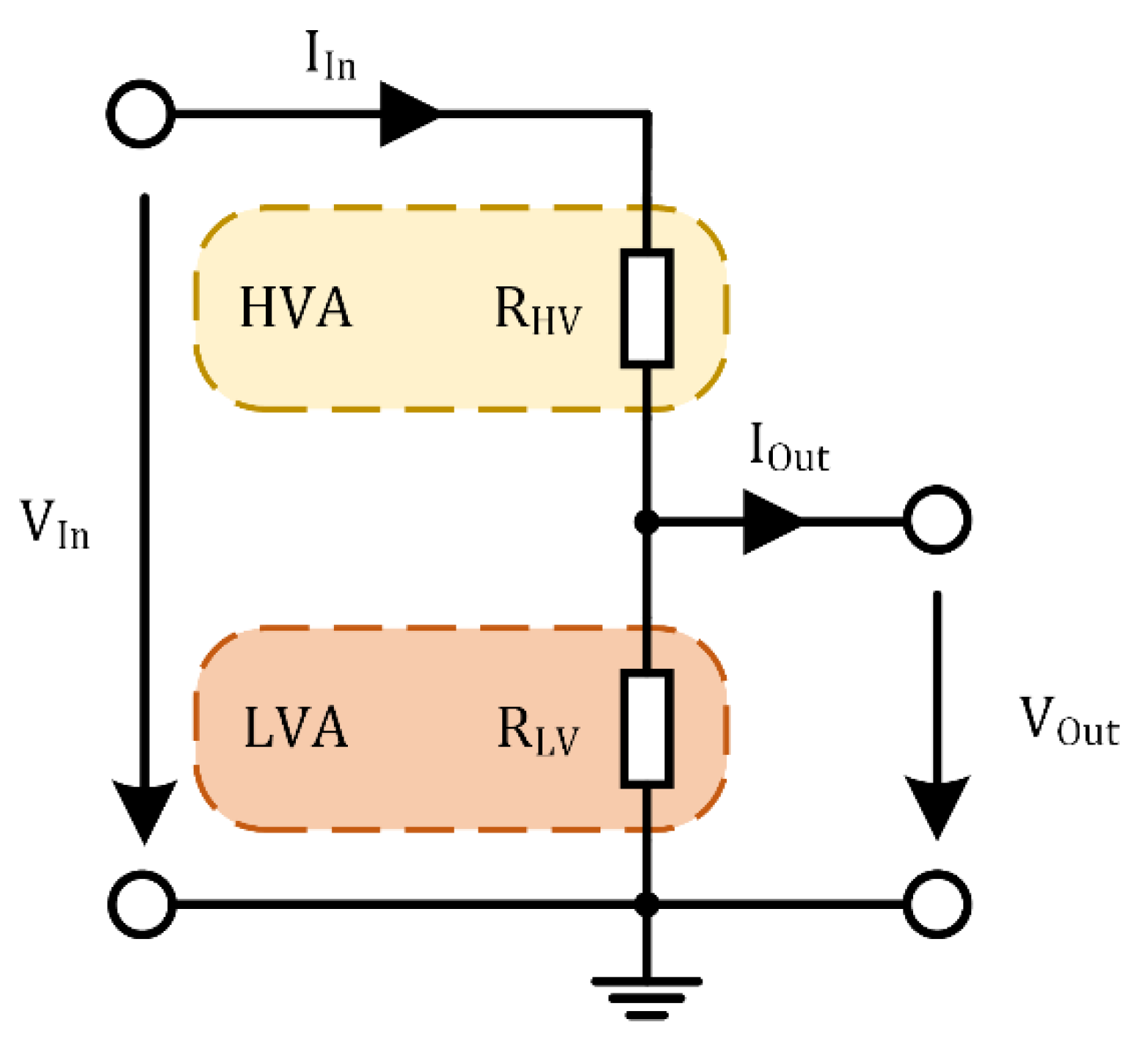
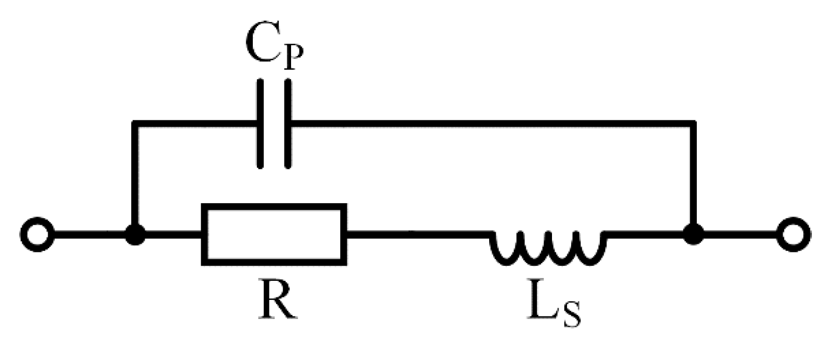
2.1. Theory of Operating Resistive Voltage Divider and Parasitic of SMD Resistors

The simplest resistive voltage divider is shown in Figure 1. It consists of two resistors with the high voltage input (VIn) and the output voltage (VOut) to be connected to the measuring device.
The upper resistor RHV, between VIn and VOut, is called high voltage arm (HVA) because most of the input voltage VIn drops here. The resistor RLV, between the output voltage VOut and the reference ground potential (GND), is called low voltage arm (LVA).
Equation (1) [16] (p. 14), [18] (pp. 39–41) can be used to calculate the attenuation of the resistive voltage divider. For the FAT-IMS, an input impedance of at least 10 MΩ was specified so that the high-voltage square-wave signal is not overloaded. The 10 MΩ input impedance results in an input current IIn of 500 µA for a high-voltage square-wave signal of 5 kV. With the attenuation of 1000:1, a resistance value of RLV = 9.99 kΩ results for the LVA.
V In V Out = R HV + R LV R LV = a
In order to measure fast transients of the high-voltage square-wave signal it is important to consider the parasitic effects. Especially for high frequencies, the parasitic effects of resistors have a significant effect on the transmission response. According to Tietze et al. [19] (p. 1325), a simple equivalent circuit shown in Figure 2 can be used for a resistor. The values for parallel capacitor CP and series inductor LS of a resistor depend on the design, the mounting technique, and package size, resulting in most likely independent of the actual resistor value [20]. For small frequencies, the resistance R dominates the impedance of the resistor, whereas for large frequencies, even for the smallest values, in the femto Farad (fF) range, CP dominates [16] (p. 274). As a result, the inductance LS can be safely neglected, especially for large resistance values R, in the range of several hundred kΩ, without changing the simulation results [21] (pp. 41–43), [22] (pp. 59–60).
If we now consider a voltage divider composed of two real resistors, it becomes clear that the parallel arrangement of R and CP forms a high-pass characteristic [19] (p. 1326). This high-pass characteristic distorts the linear transmission response of the resistive voltage divider and is mainly caused by the parasitic capacitance CP, which is almost identical for resistors with the same design but different resistance values [3,23] (p. 54).
For a frequency of 10 MHz, the complex impedance for two different resistors with a value of 1 MΩ and 10 kΩ in identical packages (size 1206) are calculated in Table 1. For a resistor in a 1206 package a parasitic capacitance of CP = 30 fF was determined using a VNA Rohde & Schwarz (Munich, Germany) ZNL6 (see beginning of Section 3. Discussion). This fits to literature values for a 1206 package, ranging from 50 fF to 200 fF [3,19] (p. 1326), Ref. [24]. In addition, for better visualization, the ratio of the impedance at a frequency of 10 MHz and the DC resistance are shown in Table 1. When comparing the ratios at 10 MHz it becomes clear that the impedance |Z| for the large resistor (nominal value 1 MΩ) has already dropped to 46.87% of the nominal value, whereas the 10 kΩ resistor still has an impedance of 99.98% of the nominal value at this frequency.

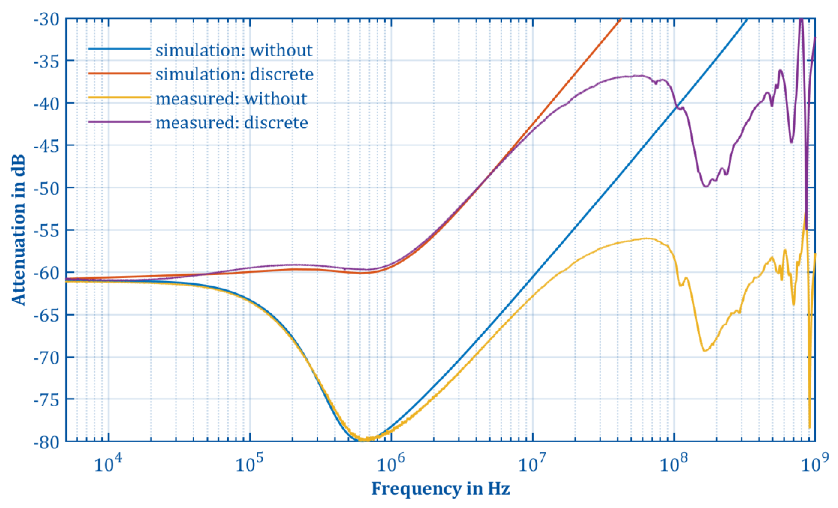
2.2. Frequency Compensation of Resistive Voltage Dividers and Resistor Selection

The different relative frequency, depending on deviations of the two resistors, cause a non-linear behavior of the resistive voltage divider. Thus, the transmission response of the resistive voltage divider is not constant over the considered frequency range. Therefore, the relative deviation from the nominal value of the various resistors must be equal for every resistor of the resistive voltage divider over the entire frequency range. To match the relative deviation of the resistors of the HVA RHV,i and the resistors of the LVA RLV over the whole frequency range, an additional capacitance CX in parallel to the LVA resistor can be added, as shown in Figure 3. The parallel parasitic capacitance CP introduced in Figure 2 is represented by the capacitors CP,I and CP,LV. The capacitors CS,i are representing the stray capacitance, formed against the surrounding environment, while the capacitors CC,i are representing the compensation electrode.
The compensation capacitor CX can be calculated according to Shi et al. [11] using the relationship shown in Equation (2). It should be considered that the capacitances cause the total impedance of the resistive voltage divider to drop significantly as the frequency increases, thus increasing the input current. In addition, it must be considered that almost the entire input voltage drops across the HVA and that this resistor must have a correspondingly high dielectric strength. Unfortunately, such high-voltage resistors have a larger parallel capacitance CP due to their design, especially if they are through hole technology (THT) devices, such as a thin film 10 MΩ resistor Ohmite SLIM-MOX10203 with a parasitic capacitance CP of 900 fF [25] (p. 1).
C X = C P · R HV N · R LV
To reduce the effect of the parasitic capacitance CP,i and at the same time ensure the dielectric strength of the HVA, the HVA was constructed from ten SMD resistors connected in series, since these generally have a lower capacitance CP than THT resistors. A series connection of several resistors also reduces the effective overall capacitance, and thus reduces the effect on the input impedance, as this is a series connection of ten RC high-pass elements.
Another parasitic capacitance to be considered is the stray capacitance CS, which also affects the transmission response. The stray capacitance CS is formed between the metalized ends of each individual resistor, the PCB trace between each resistor, and the surrounding environment [3]. These separate stray capacitances CS,i (referring to Figure 3) together with the resistive elements (resistors and PCB trace) form a chain of RC low-pass filters. To compensate for these stray capacitances CS,i, it is important that the stray capacitances remain constant in various measurement environments. Stated differently, no change in the stray capacitances should be caused by objects in the environment such as conductive objects, surfaces, or persons nearby. A constant environment, and thus constant stray capacitances CS,i, can only be achieved by a metallic shield with a fixed potential [26], realized by a brass housing, which, at the same time, provides electromagnetic shielding against the environment.
The simple equation for calculating a cylindrical capacitor is shown in Equation (3) [16] (p. 323).
C cyl = 2   π   ε 0   ε r l ln r 2 r 1
Due to the complex geometries and the edge effects of the resistors and PCB traces, only a rough estimation for the stray capacitance CS,i can be obtained here by the model of a cylindrical capacitor. The diameter r1 of the inner electrode was approximated by the width w of the resistors since the conductor between the resistors can be made much smaller and are not as important. The diameter of the outer electrode r2 corresponds to the inner diameter of the brass housing. For the length l, the length of a single SMD resistor was used for the first estimation. To compensate for the low-pass behavior of the resistive voltage divider caused by the stray capacitance CS,i, an additional capacitance between the nodes and the input potential is introduced, as previously described by Shi et al. [11]. If the stray capacitance is known, the compensation capacitance CC,i can be determined according to Equation (4).
C C , i = C S , i ( N · a i   ( a 1 ) 1 )
Based on Shi et al. [11], the schematic shown in Figure 3 was developed for the entire resistive voltage divider, with a number of N = 10 HVA resistors. The capacitance CC,i of the compensation electrode compensate for the charge at the stray capacitance CS,i when the potential at each node ki changes differently. To accomplish charge neutralization, the capacitance CC,i must decrease as the index i increases. For the selection of a specific resistor package, different sizes from 0402 (length l = 1.02 mm and width w = 0.5 mm [23] (p. 51)) to 2010 (length l = 5.08 mm and width w = 2.54 mm [16] (p. 273)) and the resulting parasitic effects were first compared with each other, and an optimal package was determined. In particular, the estimated stray capacitances CS,I and the minimum number of resistors required for voltage stability were evaluated, and the expected rise time without frequency compensation was used as a measure for the expected input capacitance. Furthermore, it was taken into consideration that the resistors should be placed in an aligned row to reduce interference and leakage current. With these aspects in mind, an optimum package size of 1206 (length l = 3.2 mm and width w = 1.6 mm [16] (p. 273)) was found for the resistive voltage divider SMD resistors. With ten of these resistors connected in series, the operating voltage of each individual resistor does not exceed the nominal value specified in the datasheet.
The small number of resistors in series offers the advantage of a less prominent low-pass behavior since there are fewer low-pass elements consisting of a resistor and the stray capacitances CS,i. This in turn leads to a smaller compensation electrode and reduces the input capacitance of the resistive voltage divider. Table 2 compares various resistors from different manufacturers in selected categories, all in package 1206. The shown values always refer to a resistor with a value of 1 MΩ and the best available accuracy. Less accuracy leads to larger tolerance of the resistors, and thus to deviations in the voltage measurement. Only resistors with thin or thick film technology were compared, as these offer the lowest expected tolerances and temperature dependencies according to [27] (p. 1107).
Due to the lower temperature dependency and frequency stability [16] (p. 273), [21] (pp. 38–39) of thin film technology resistors, their lowest absolute tolerance, and the highest power dissipation, the SMD resistor Vishay PTN1206E1004BBT1 was selected for the resistive voltage divider setup.

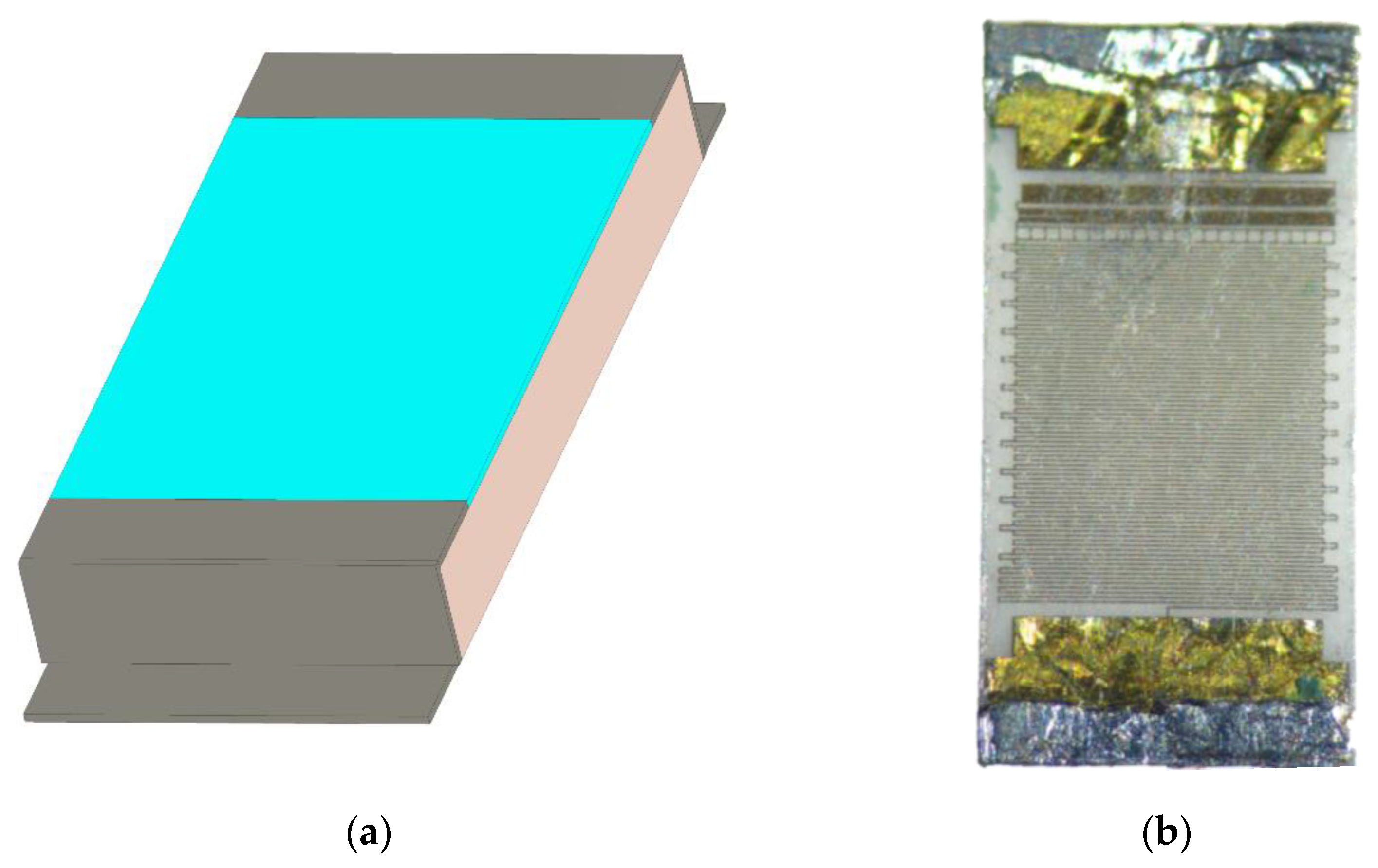
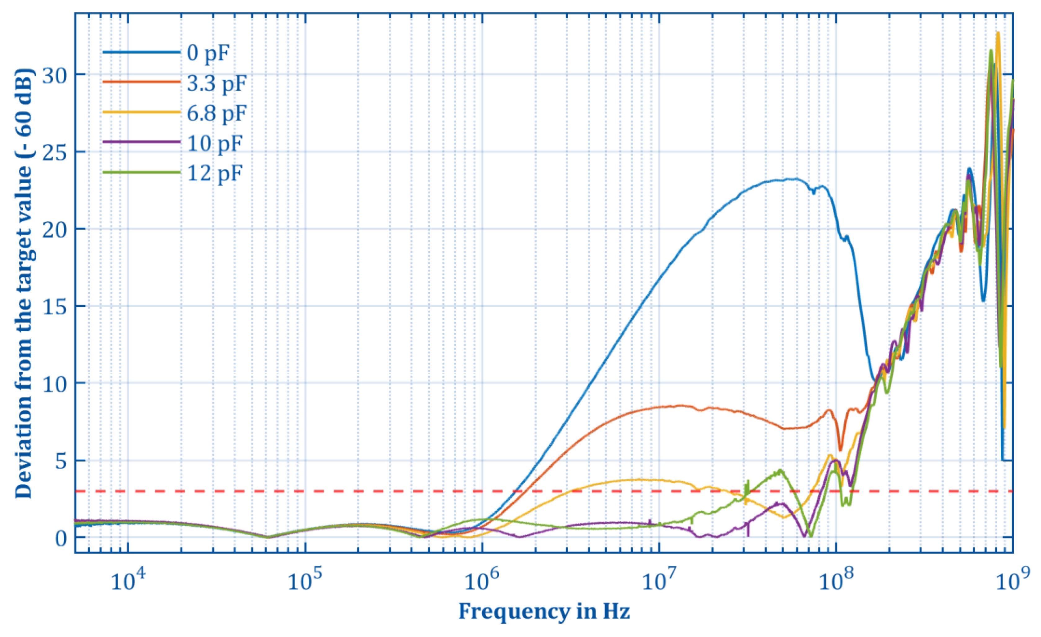
2.3. Simulation of Resistors and Resistive Voltage Divider

Compared to the application described by Shi et al. [11], which uses a resistor in the form of a ceramic tube cylinder with a specially shaped metallic torso compensation electrode inside, a compensation electrode based on the adjacent PCB layer is used here. The compensation electrode built from the structured copper layers on one side of the PCB forms a capacitor with the SMD resistors and traces on the adjacent side that is determined by the dielectric constant of the PCB material, the thickness of the PCB, and the area and geometry of the compensation electrode. A sufficiently high dielectric strength is ensured by the PCB material FR4 used as the dielectric material with an insulation strength of 45 kV/mm [33] and the selected SMD resistors, which means that no holes or vias are required. The necessary capacitances CC,i for compensation of the stray capacitances CS,i can be calculated with Equation (4) according to Shi et al. [11], assuming that all stray capacitances CS,i are the same for the individual sections in the model.
The calculated discrete compensation capacitances CC,i serve as a first estimation for the dimensioning of the compensation electrode. Based on this estimation, different compensation electrode geometries were designed and investigated.
According to the geometry of the compensation electrode of Shi et al. [11], a pentagonal compensation electrode was first investigated in the Dassault Systémes CST Studio Suite 2021® Microwaves and RF solver. Further simulations in the Dassault Systémes CST Studio Suite 2021® Microwaves and RF solver have led to other promising compensation electrode geometries for a constant transmission response. All compensation electrode geometries allow for a significant reduction of the low-pass behavior. The compensation electrode geometries are shown schematically in Figure 4. The compensation electrode geometries (Figure 4a,b) perform well in the simulations, but might have one major drawback in practice since the position accuracy of the resistors affects the compensation capacitance to a high degree. However, the discrete compensation electrode geometry (Figure 4c) does not show this drawback since two copper surfaces are adjacent to each other, with minor deviations of roughly ± 10 µm due to variations in production [34,35], thus forming a capacitor.
A simplified geometric model of the resistors was used for the field simulation in the Dassault Systémes CST Studio Suite 2021® Microwaves and RF solver. The real resistor, as shown in Figure 5b, has a meander-shaped thin current path, vapor deposited on the alumina substrate. The model in the Dassault Systémes CST Studio Suite 2021® Microwaves and RF solver is also made of an alumina substrate as shown in Figure 5a. Instead of the meanders, the model is designed with a thin, planar conducting cuboid, since this simpler structure significantly reduces the simulation complexity and time. Furthermore, the meander structure differs for each individual resistor due to the trimming process in manufacturing, leading to an individual shape for each resistor. This simplification affects the stray capacitance, due to the larger surface area but reduces the parasitic parallel capacitances CP of the resistor. The deviation between the simulated and the real resistor can be seen in Figure 9, but it is low and can be neglected, as shown later in the discussion.
The geometry of the metallization at the end faces of the resistors was also simplified and only consist of three rectangular metallization instead of the complex shaped geometry (see Figure 5b) with even different martial layers. All other parameters such as the parasitic inductance Ls were considered with the geometries used in the model, but probably do not fully correspond to the real behavior of the resistor.
To simulate and evaluate the low-pass compensation, the impedance of the HVA consisting of ten individual resistors, was simulated in a metallic case for a frequency from 5 kHz to 1 GHz for all three geometries shown in Figure 4 and for a PCB without compensation electrode. By taking the metallic case into account, the effect of the stray capacitance CS,i can be simulated and thus the effect of the compensation can be shown. All electrically conducting structures were modeled as perfect electrical conductors, which is valid for the copper traces or the shielding housing made of brass. By using perfect electrical conductors in the model, the simulation time could be significantly reduced while still providing sufficiently accurate results. This simplification should not have a significant effect on the simulated results, because the effective absolute resistance of the conducting structures in the high voltage arm, except for the resistive sheets (representing the meanders from the real resistors) are very small compared to the overall resistance of the high voltage arm. This also applies to the brass housing, because the dimensions of the enclosure give a resistance in the mΩ range.
The simulated model of the resistive voltage divider is shown in Figure A1 in the Appendix A.
To compare the different compensation electrode geometries and determine the effectiveness of the low-pass compensation, the simulated transmission responses of the HVAs of the resistive voltage dividers in a frequency range from 10 kHz to 10 MHz are shown in Figure 6. The influence of the low-pass compensation becomes particularly clear when the curve without compensation (blue) is compared with the compensated curves of the pentagonal (red), discrete (yellow), and rectangular (purple) compensation electrodes. The deviation from the nominal impedance of 10 MΩ (equivalent to −100 dB when normalized to Z0 = 50 Ω) is significantly reduced up to a frequency of 1.5 MHz. In the simulation, the discrete compensation electrode geometry offers the best frequency response, but in comparison to the other geometries, the transmission response of the discrete compensation electrode geometry tends to increase at a frequency of 1 MHz. Reaching a truly flat transmission response curve for the resistive voltage divider with this simple compensation approach is not possible, due to the occurring edge and scattering effects. A significantly more complex three-dimensional structure of the compensation would be necessary as suggested by Shi et al. [11]. However, due to the similar promising results for all compensation electrodes and, eventually, limited accuracy of the simulation due to the assumptions made, all three simulated compensation electrode geometries were built and investigated experimentally.
With every compensation electrode geometry shown in Figure 6 a compensation is possible up to a frequency of about 1.5 MHz, for higher frequencies, a high-pass behavior is visible in all transmission responses. This high-pass behavior was investigated and iteratively reduced by placing the additional capacitance CX (see the next section).

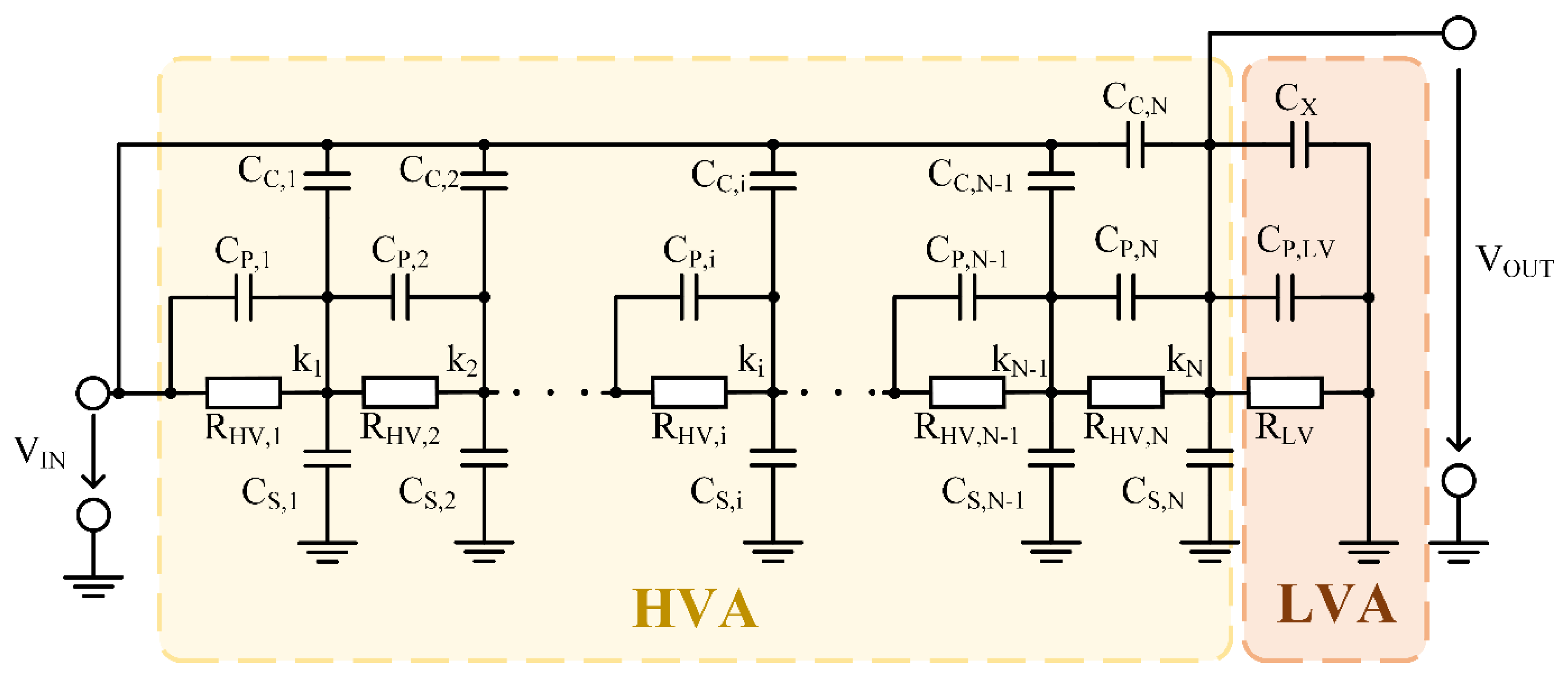
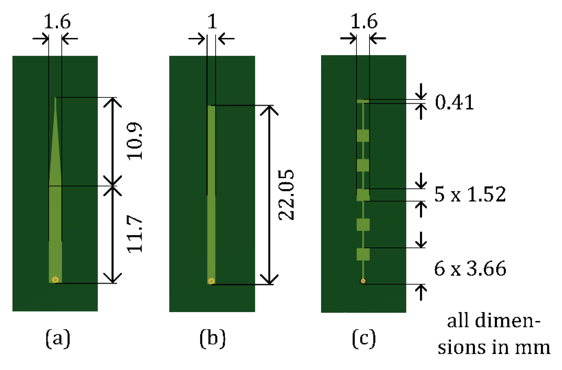
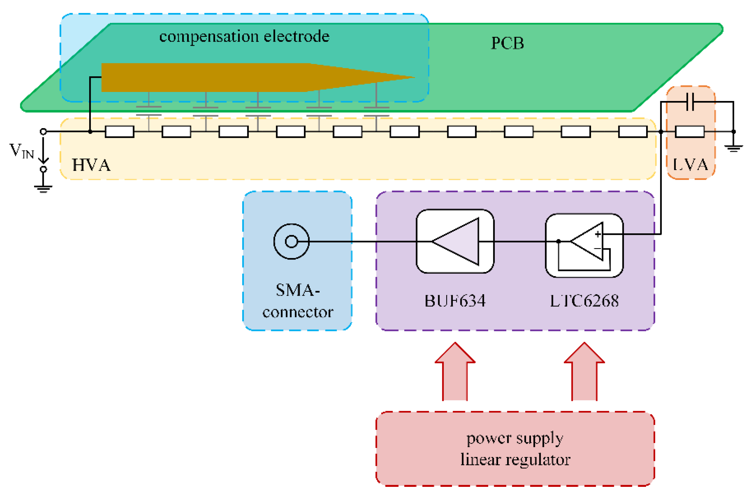
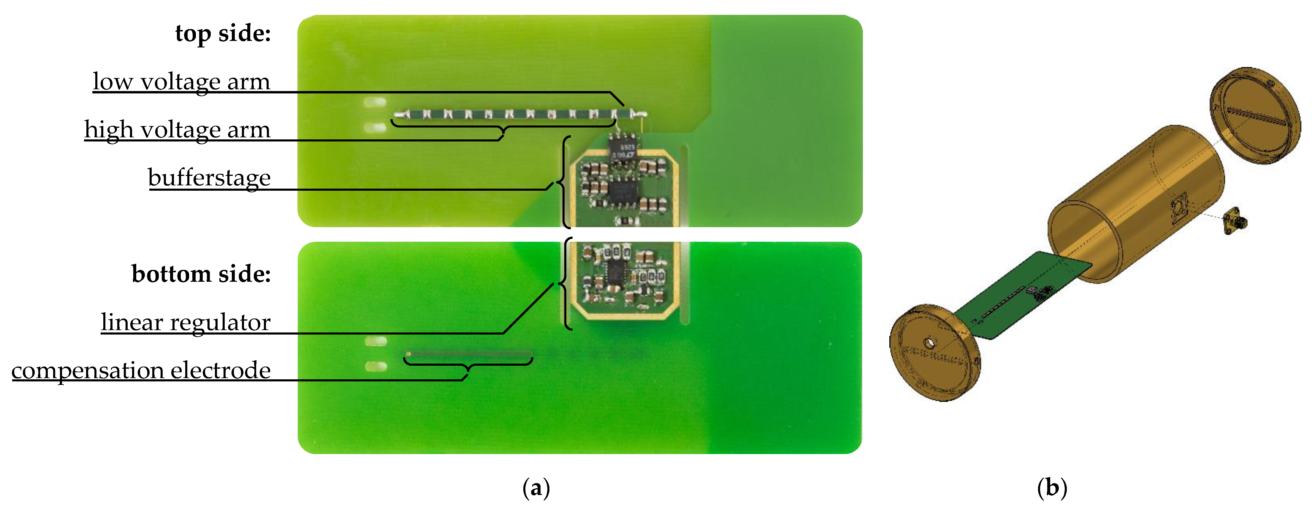
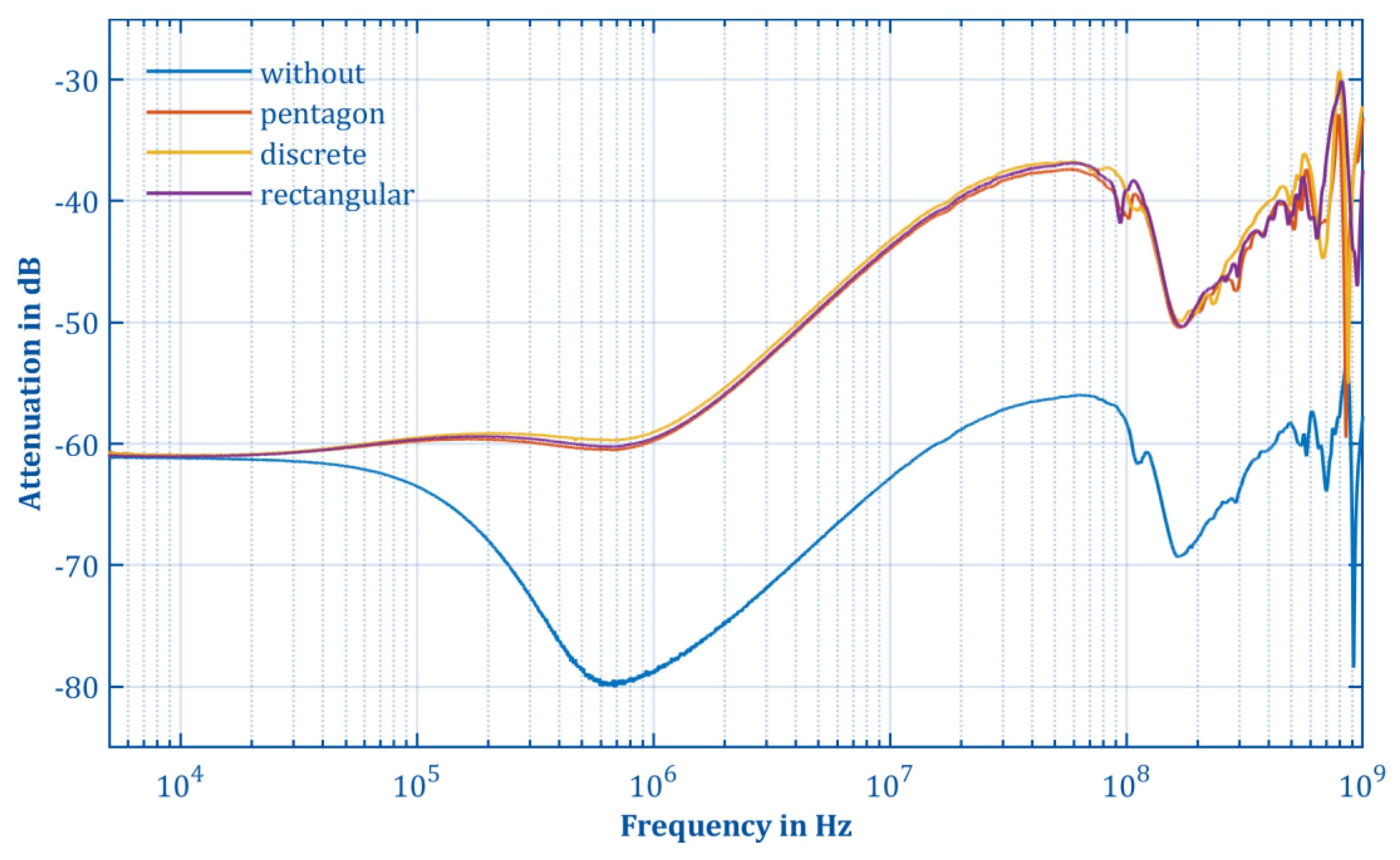
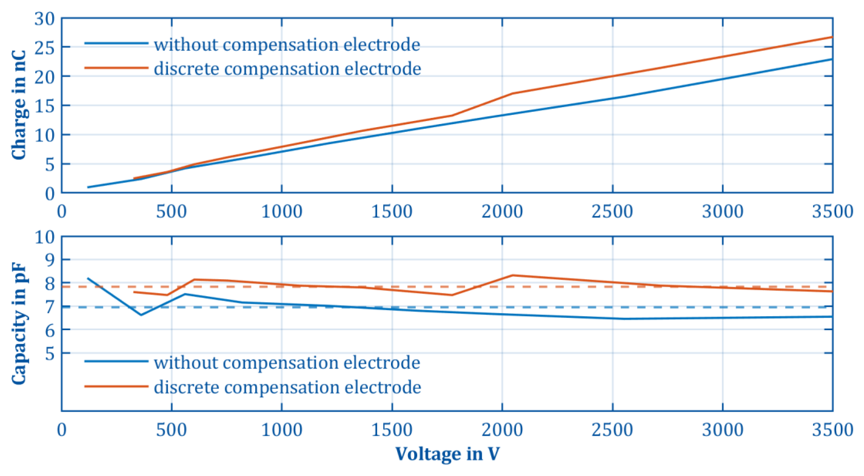
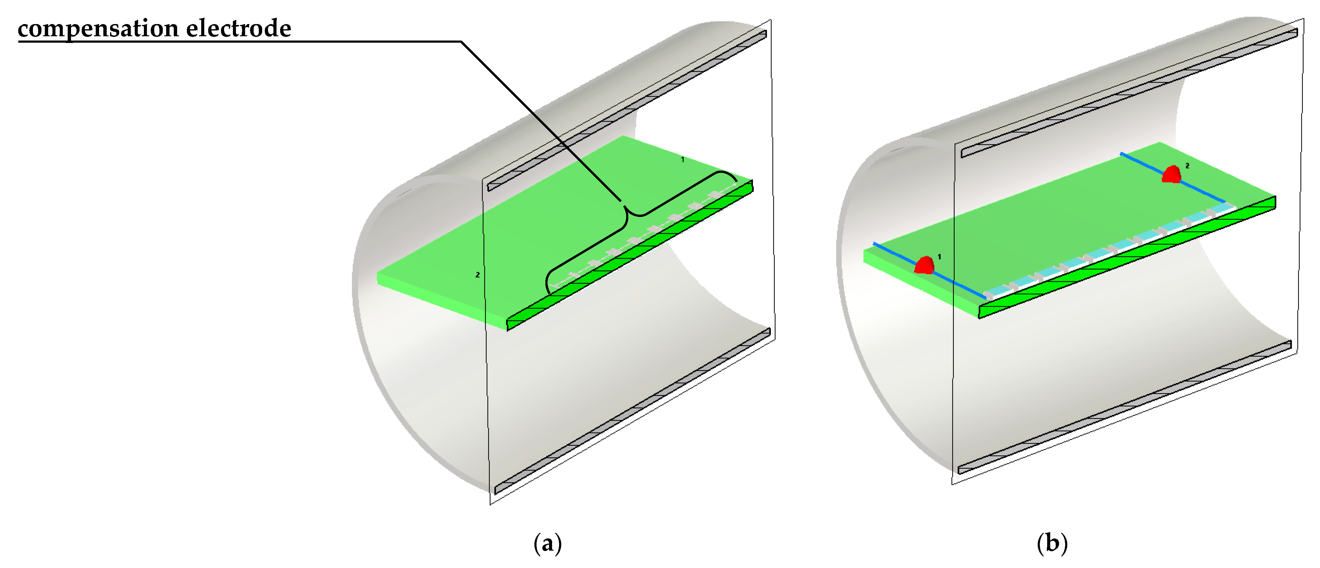
2.4. Design of the Resisitve Voltage Divider

For the resistive voltage divider to be linear over a large input voltage range, the same current through the HVA and the LVA is needed. A minimal deviation from this, combined with the high overall impedance of the resistive voltage divider, can distort the linear transmission response. Therefore, a buffer stage was placed between the output voltage and measuring device so that the current flowing into the measurement device does not affect the attenuation and the linear transmission response of the resistive voltage divider. In addition, this also makes it possible to use measurement devices with an arbitrary input impedance, for example, a VNA with 50 Ω. The buffer stage consists of an operational amplifier Linear Technology LTC6268 with a very low input capacitance of 450 fF and input current of ±3 fA according to the datasheet [36]. After the operational amplifier, a high-speed buffer Texas Instruments BUF634 is connected in series with a sufficiently large output current, to drive the 50 Ω inputs of the measurement devices. The power supply for the operational amplifier and the high-speed buffer is provided by an integrated low noise voltage regulator Linear Technology LT3032 and placed on the compensation electrode geometry side of the PCB. The block diagram of the resistive voltage divider with all compensations, power supply, and buffer stage, but without the brass housing is shown in Figure 7. Detailed schematics with all components can be found in Figure A2 in the Appendix A.
Another way to estimate the performance of the resistive voltage divider is the signal to noise ratio (SNR). In the theoretical analysis, only the thermal noise was considered for the resistors in the HVA and LVA, which Johnson [37] and Nyquist [38] found to be VR,th,rms = 12.767 mV for the input resistance of 10 MΩ at a considered bandwidth Δf of 1 GHz, and an assumed temperature of 22 °C. Additionally, the current noise is very low due to the used thin film resistors and the low current through the resistors [29] and can easily be neglected. To determine the total output noise at the SMA connector a Gaussian error propagation was applied. Therefore, the noise of the buffer stages must also be determined and considered. For a frequency range from 10 Hz to 1 GHz, the noise voltage for the operational amplifier Linear Technology LTC6268 is VLTC6268,rms = 0.155 mV [36] and for the high-speed buffer Texas Instruments BUF634 VBUF634,rms = 0.126 mV [39], the input-referred current noise of the amplifiers can be neglected due to the lower influence by a factor of 1000 compared to the voltage noise. This results in a total output noise of Vtot,rms = 12.769 mV. With a confidence interval of 99.7% (6 σ) and an output amplitude of ±5 V, this results in an SNR of 42.31 dB or an input-related peak-to-peak noise of 38.307 V. Thus, when designing the resistive voltage divider, a compromise needs to be found between input impedance, usable bandwidth, and noise.
Figure 8a shows the assembled resistive voltage divider with the ten SMD resistors forming the HVA and one single SMD resistor for the LVA, as well as the amplifier circuit. The compensation electrode and the linear power supply are on the bottom layer of the PCB and therefore not visible. In addition, the compensation capacitor CX sitting above the LVA resistor is not placed yet for better visibility. The exposed U-shaped copper area in the lower middle of the PCB is provided to attach an electrical shield around the amplifier electronics consisting of a grounded copper foil, thus reducing electromagnetic interference. The assembled board is held in place by a milled pocket in the two end caps of the cylindrical brass housing. Figure 8b shows an exploded view of the resistive voltage divider containing the PCB with the resistors and buffer stage, the brass housing, the high-voltage connection, and the low-voltage output. A Photo of the assembled resistive voltage divider is shown in Figure A3 in the Appendix A. The connection of the measuring device is fed through the housing wall by an SMA socket. The high-voltage is fed through the hole in the front cap. For this purpose, a non-shielded high-voltage cable is used for insulation of the high-voltage to minimize the input capacitance compared to a shielded high-voltage cable. However, a shielded high-voltage cable can be also used if required.

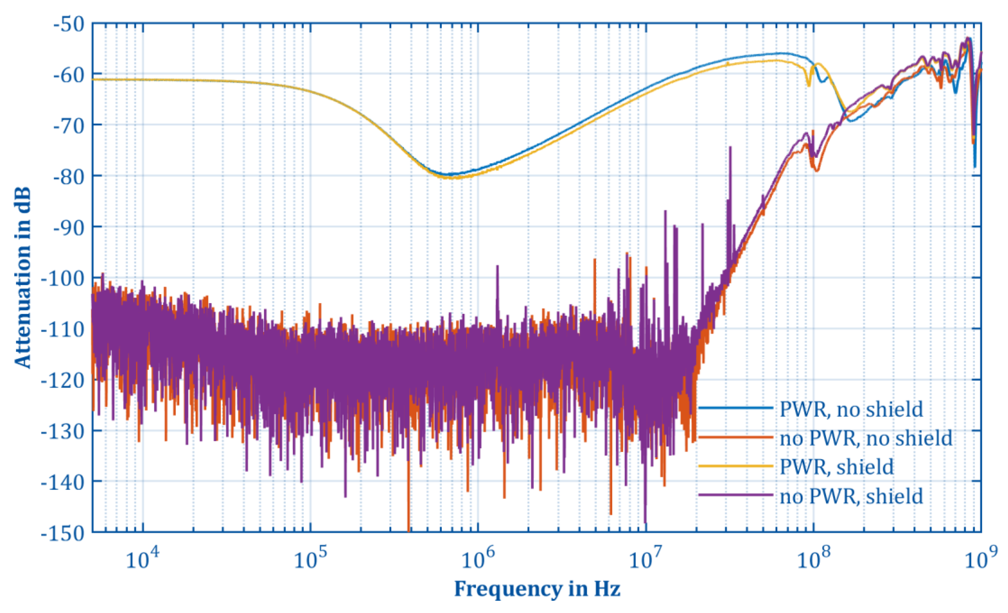
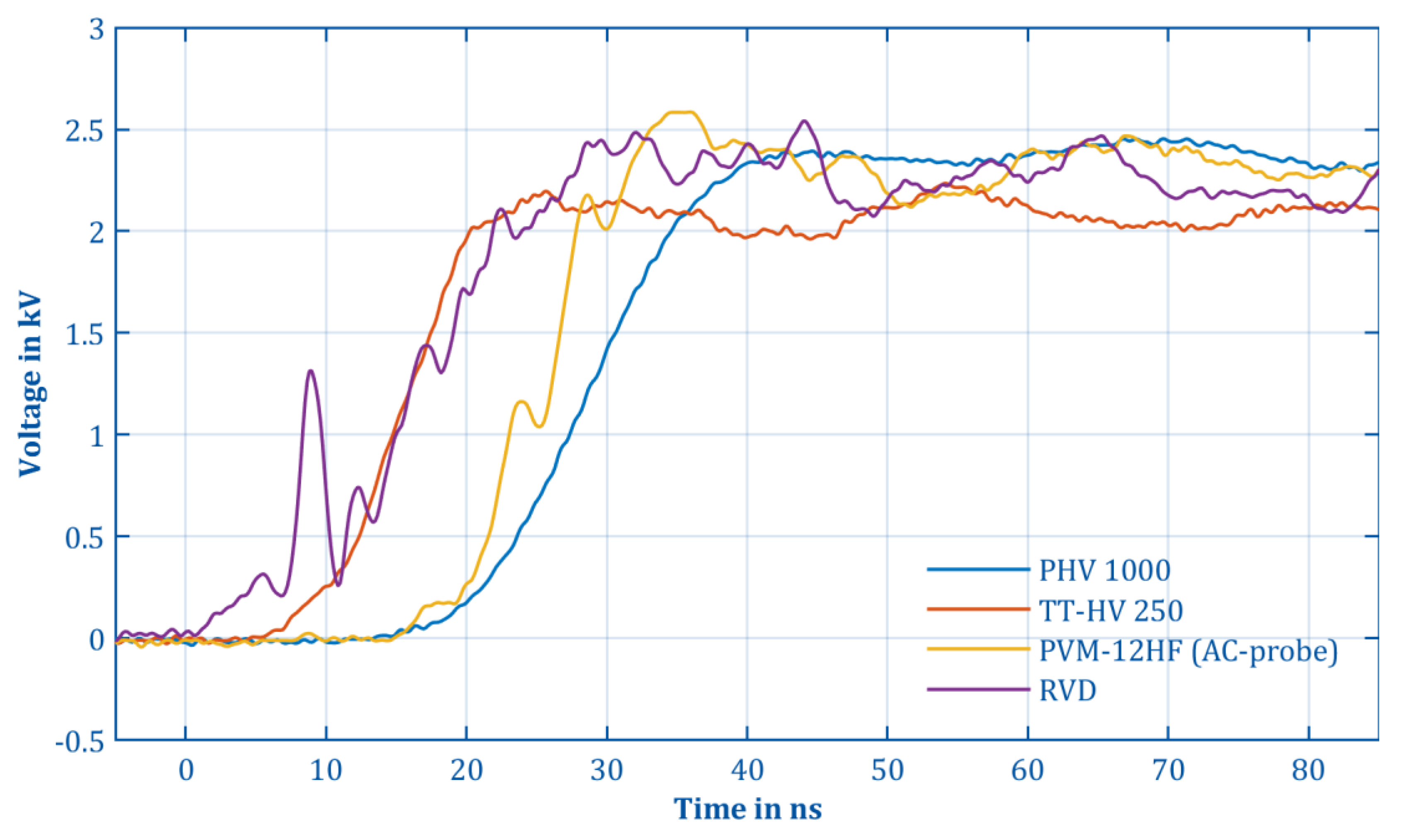
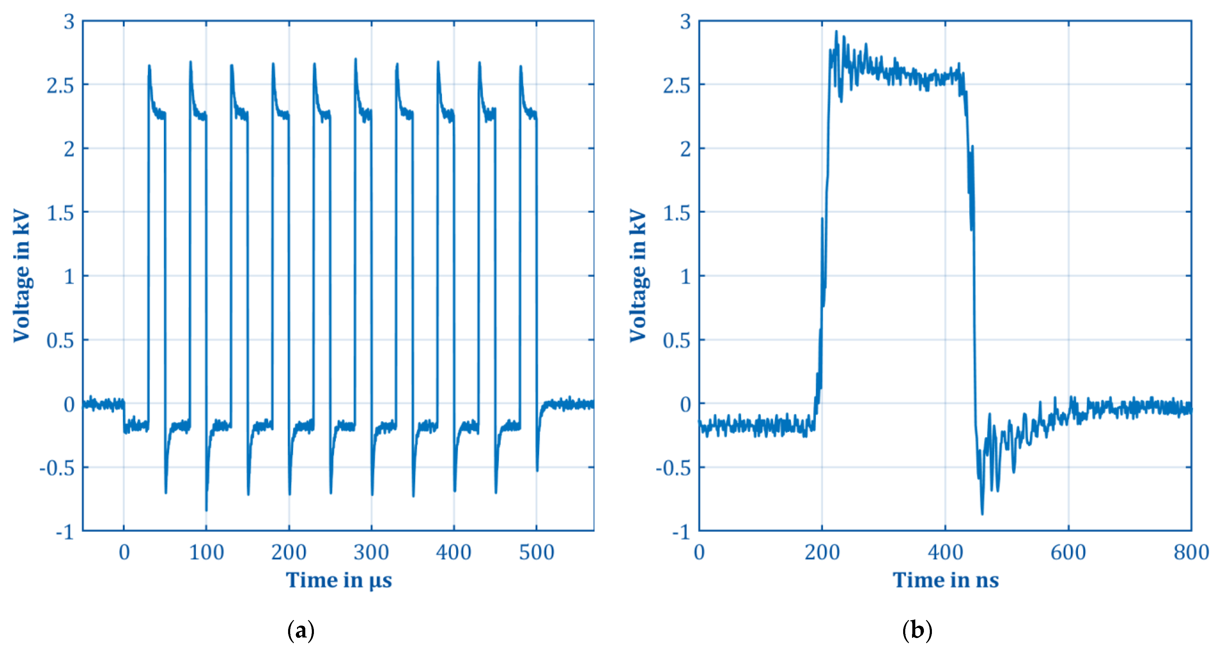
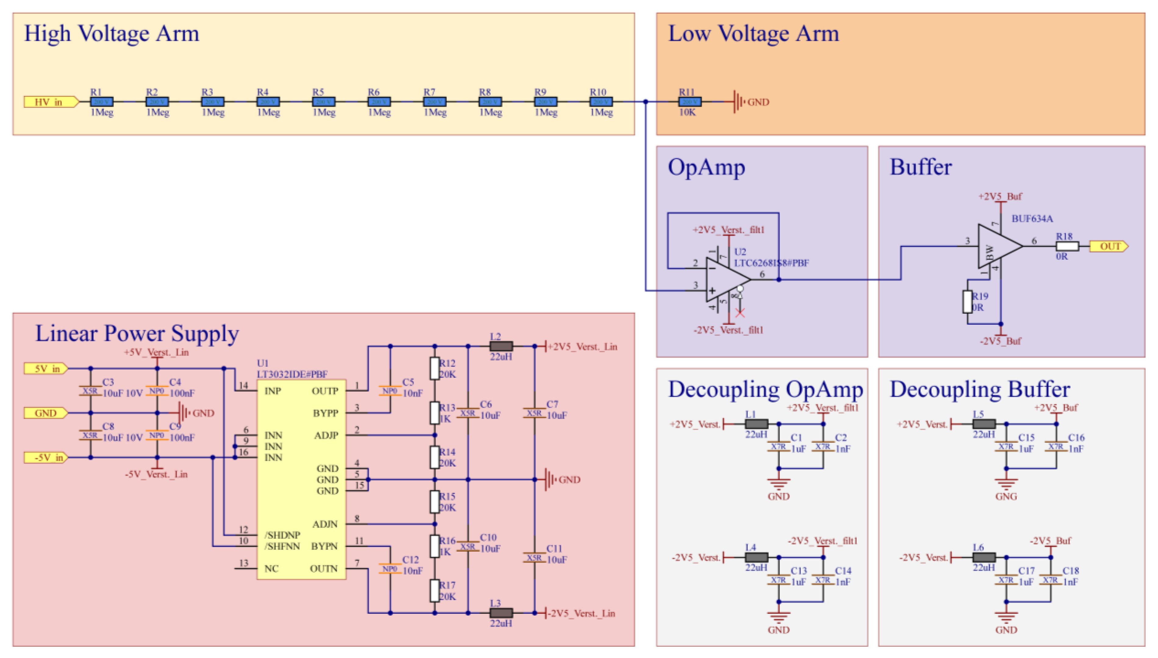
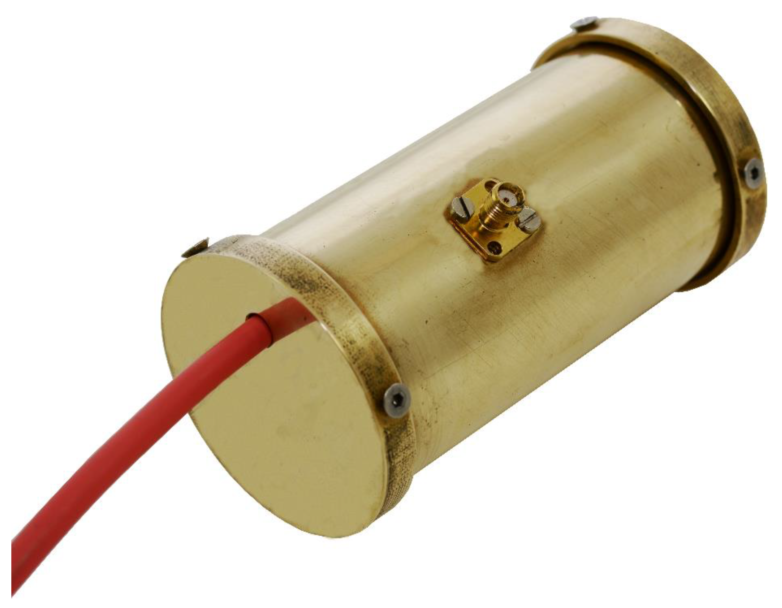
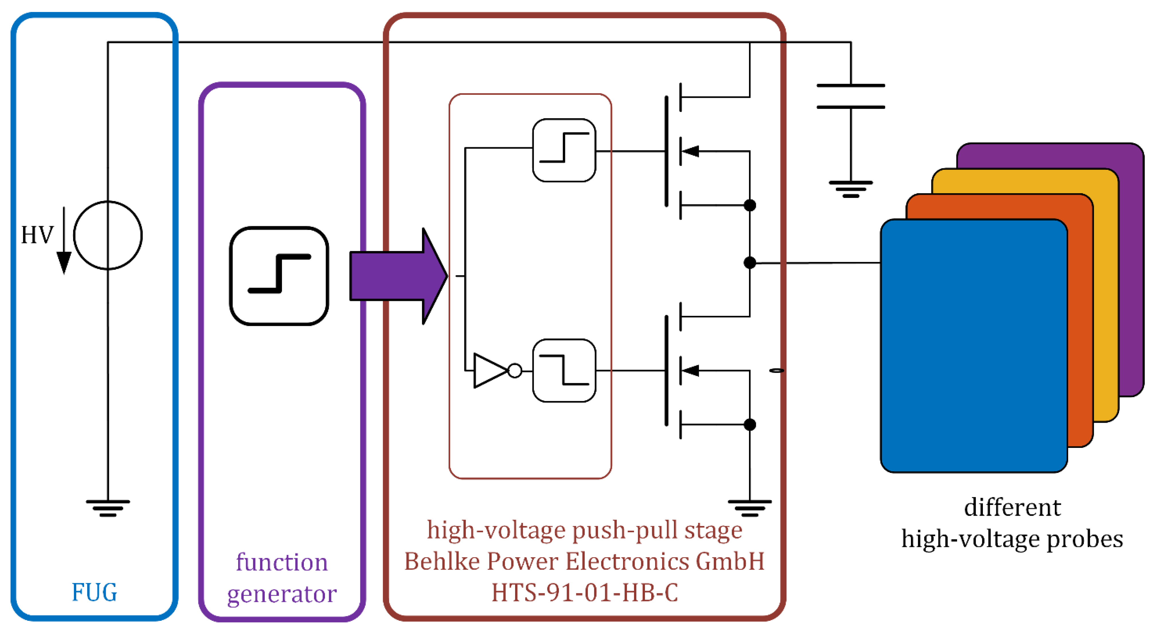
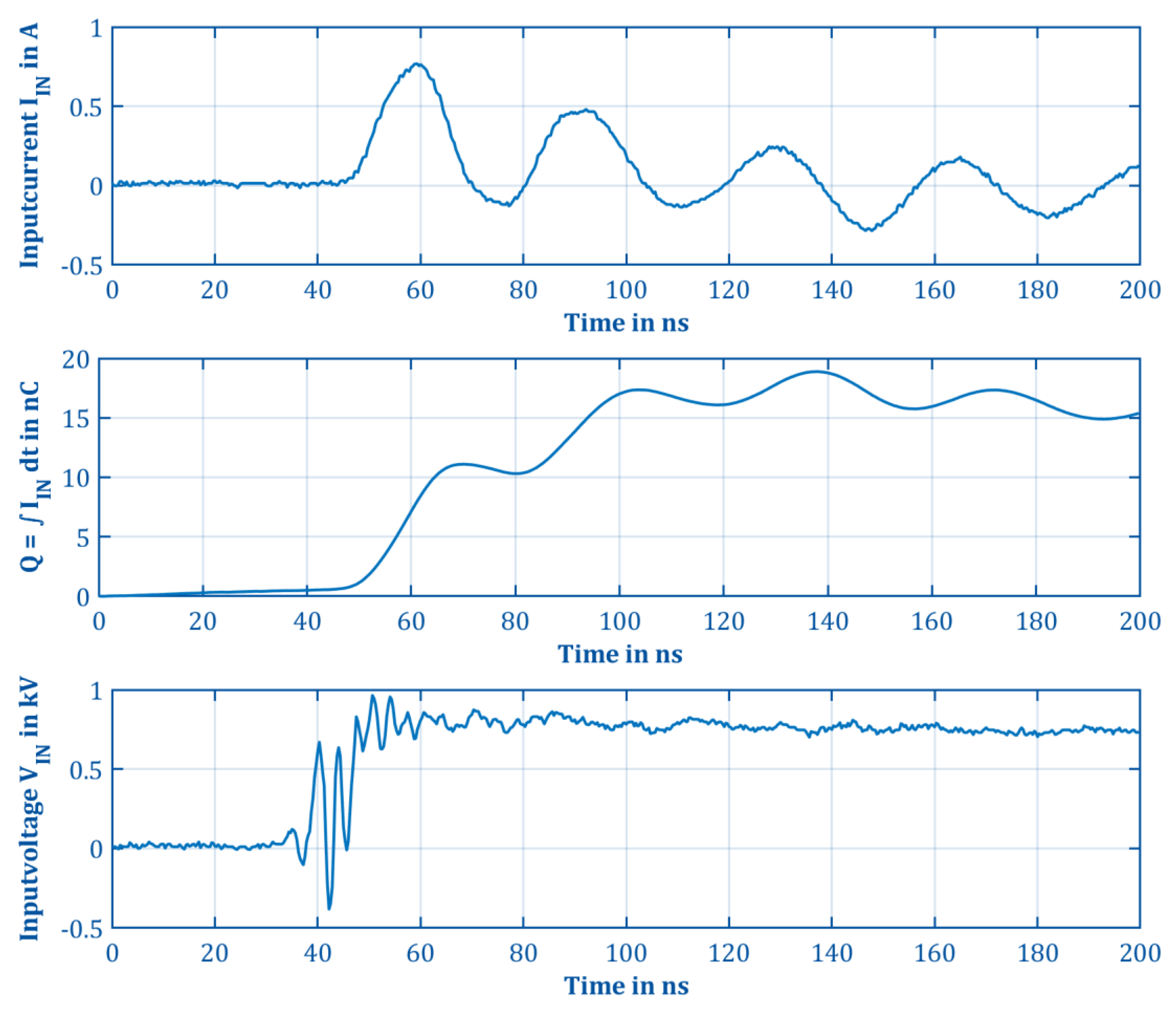
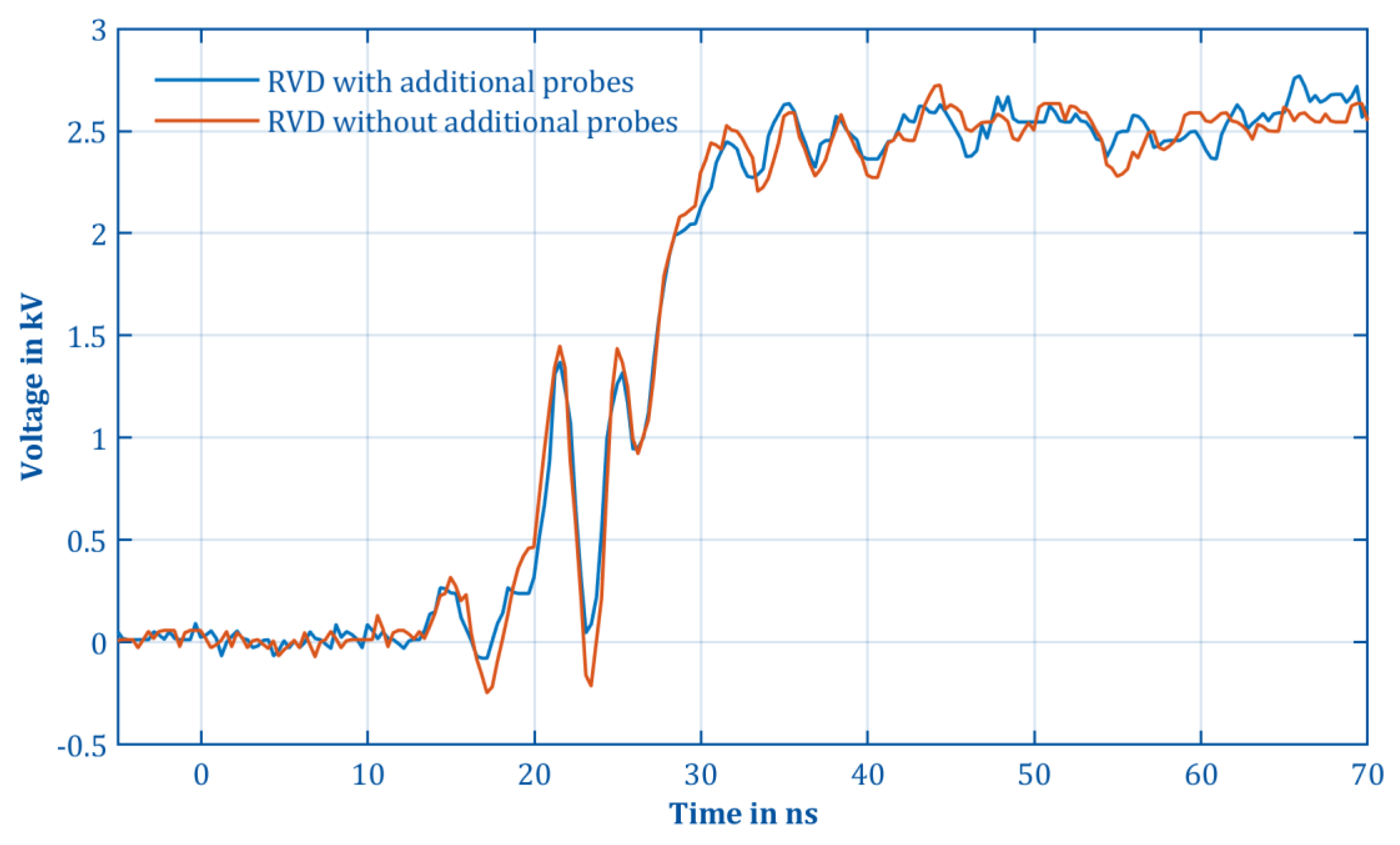
2.5. Measurment Setups
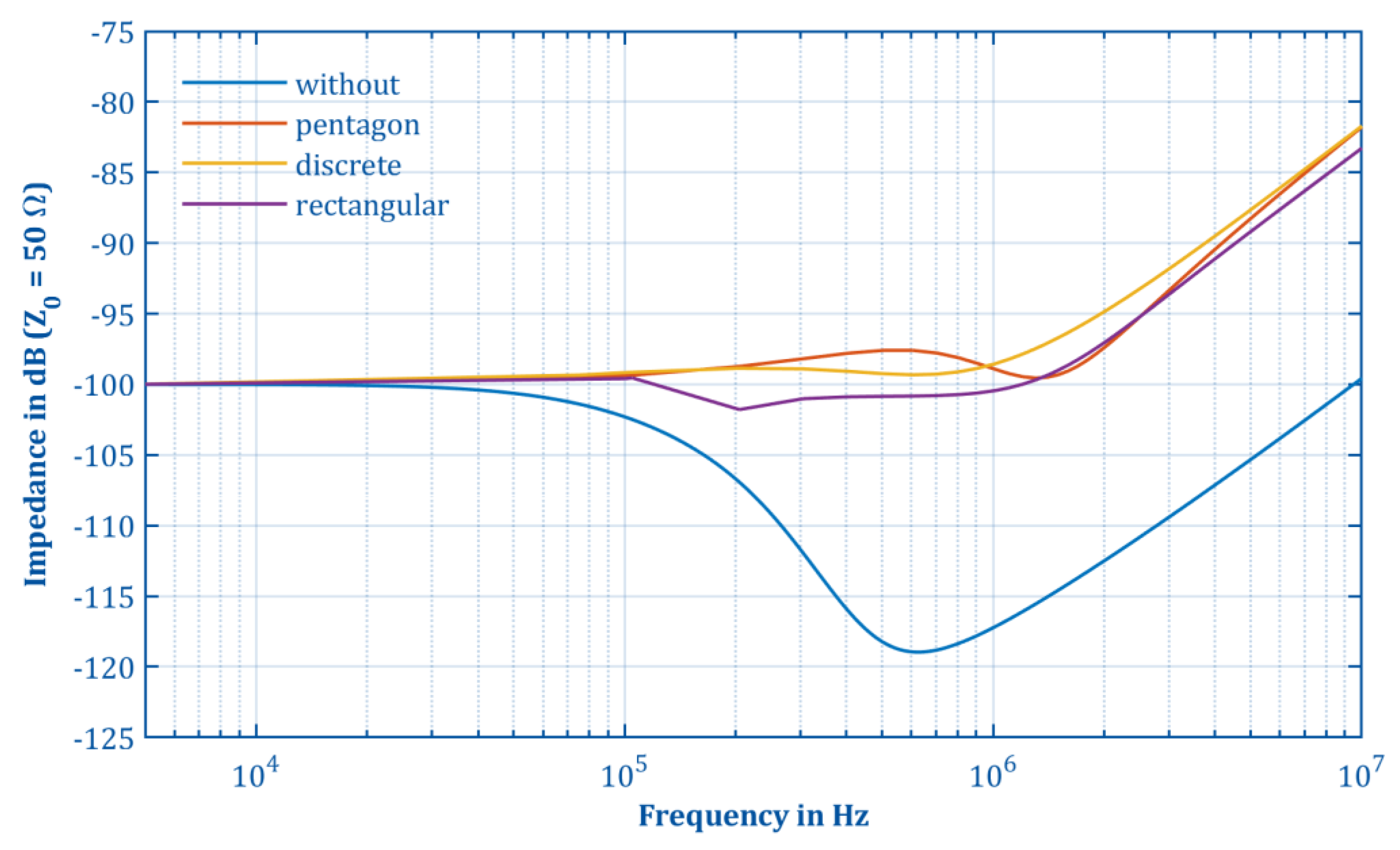
A VNA Rohde & Schwarz ZNL6 was used to measure the transmission response of the resistive voltage divider. The VNA and the matching cables Rohde & Schwarz ZV-Z192 were calibrated with a Rohde & Schwarz ZN-Z135 calibration kit.
A high-voltage push-pull stage Behlke Power Electronics GmbH HTS 91-01-HB-C was used to measure the transient response. The high-voltage used for the supply of the high-voltage push-pull stage was generated by a high-voltage power supply FUG Electronics GmbH (Schechen, Germany) HCP 35–3500 and an additional 0.1 µF high-voltage film capacitor WIMA FKP 1 0.1 µF 6000 V DC, placed close to the high-voltage push-pull stage, to generate sharper switching edges, as shown in Figure A4 in the Appendix A. According to the datasheet, the rise time of the high-voltage push-pull stage is approximately 12 ns from 0 V to 2.5 kV [17]. The voltages measured with the high-voltage probes were recorded using an oscilloscope Keysight MSO4104A with a bandwidth of 1 GHz and up to 6 GS/s. For comparison, the high-voltage transient was recorded simultaneously with an AC probe North Star High Voltage (Bainbridge Island, WA, United States) PVM-12HF [40] and two DC probes—Testec Elektronik GmbH (Dreieich, Germany) TT-HV 250 [13] and PMK Mess- & Kommunikationstechnik GmbH (Bad Soden am Taunus, Germany) PHV 1000 [12]. Table 3 compares the major parameters of the used commercially available probes.
To measure the effective input capacitance of the developed resistive voltage divider, the transient measurement setup was used, without the commercially available high-voltage probes. During the voltage change, the current flowing into the resistive voltage divider was recorded with a current clamp from Agilent 1147B, with a bandwidth of 50 MHz. The effective input capacitance is obtained from the quotient of the charge flowing into the resistive voltage divider and the amplitude of the voltage change. To determine the charge from the measured current, the integral covers a time period of 200 ns around the transient. This process is repeated for different voltages. For each operating point, the capacitance is determined from the quotient of the charge and the voltage using Gauss’ law. Figure A5 in the Appendix A shows an exemplary plot of the input voltage, the input current, and the charge integral for a transient with an amplitude of the voltage change of 2.154 kV. The calculation neglects the DC current flowing through the resistive voltage divider as a function of the applied input voltage. Thus, the value for CIn is estimated too large. However, the following worst-case estimation shows that the influence of the DC current is negligible: For an input voltage of 3.5 kV, a constant DC current of IIn = 350 µA would occur with an input impedance of Rin = 10 MΩ. In the considered time interval of 200 ns, a charge difference of 70 pC results, which can be neglected compared to the measured charge differences of several nC due to the input capacitance.

3. Discussion

To verify the simulations conducted with the Dassault Systémes CST Studio Suite 2021® Microwaves and RF solver, the transmission and reflection parameters of a single 1 MΩ Vishay PTN1206E1004BBT1 resistor were measured with the VNA and compared to the simulation. The parameters used for the measurement with the VNA ZNL6 are listed in Table A1 in the Appendix A. The results of the measurement and simulation of the transmission response parameters are compared in Figure 9 over a frequency range from 5 kHz to 1 GHz. The measured transmission response of the resistor (PTN1206E1004BBT1) in blue corresponds well to the simulated curve in red up to 2 MHz, verifying that the model is valid up to this frequency. Above a frequency of 2 MHz, a high-pass behavior becomes visible in both the experiment and the simulation, which is most likely caused by parallel parasitic capacities CP,i.
From the measured response, an equivalent parallel capacitance CP = 30 fF can be determined from Equation (5) for high frequencies at which the parasitic parallel capacitance is dominant as shown in Figure 9. For the previously considered behavior from the simulation, a similar high-pass behavior occurs from about 4 MHz and the equivalent capacitance CP can be determined to CP = 22.2 fF using Equation (5).
| 1 1 R + j ω C | = | Z ¯ | | C | = | j ( | Z ¯ | + R ) ω   R   | Z ¯ | |
The deviating transmission response of the simulation model is most likely caused by the simplified assumption that in the real resistor the current path on the resistor is not as straight as in the simulation model, but rather meander-shaped. Therefore, capacitive coupling between the individual sections likely causes this effect in the simulation, which increases the total effective parasitic capacitance CP compared to Figure 5. Effects based on electromagnetic fields, like the skin effect, are considered due to the field-based simulation in the Dassault Systémes CST Studio Suite 2021® Microwaves and RF solver. Furthermore, the skin effect should not have a significant influence, because the thickness of the resistive trace on the resistor is within 50 nm [41] (p. 4) and thus way smaller than the skin depth in copper even for high frequencies such as 1 GHz with a skin depth of 2.06 µm [42] (p. B14). However, the deviation is so small that the simplified model was used for the development of the resistive voltage divider to save simulation time.
The impedance of the resistive voltage dividers each consisting of ten 1 MΩ SMD resistors in the HVA, one 10 kΩ resistor in the LVA, the active buffer circuit (Figure 7), and the different compensation electrode geometries shown in Figure 4 were simulated and then measured over a frequency range from 5 kHz to 1 GHz. Due to the active buffer stage, it is also possible to measure the actual transmission response of the resistive voltage dividers with the 50 Ω terminated VNA ZNL6. The parameters for measuring the transmission responses with the ZNL6 are identical to those for measuring the individual resistor and can be found in Table A1 in the Appendix A.
The measurements enable the evaluation of the compensation electrode and the low-pass behavior caused by the stray capacitance (CS,i in Figure 3). The transmission response is shown in Figure 10. To evaluate the effect of the compensation electrode geometries, a setup without a compensation electrode was also investigated. The (blue) curve shows the transmission response for the uncompensated setup, with a clear attenuation of the signal above 100 kHz. The curves for the pentagonal (orange), discrete (yellow), and rectangular (violet) compensation electrodes no longer exhibit any low-pass behavior and are largely constant up to about 1 MHz. From this frequency on, the high-pass behavior dominates due to the concatenation of the parasitic capacities CP. Very similar behavior is also visible in the transmission response of the uncompensated resistive voltage divider. The determination of the effective parallel capacitance and the stray capacitance in the simplified model strongly depends on the frequency and the used model for approximation. Furthermore, the determination of the effective parallel capacitance and the stray capacitance from the measured values is not reasonable, since the low-pass and high-pass behavior in the transfer function are interfering.
Very similar behavior for frequencies of up to 10 MHz can also be seen in the simulation results in Figure 6. It should be noted that in Figure 6 the transmission response was determined only for the HVA and the graph in Figure 10 shows the S21 parameter. For a 2-port system, S21 is defined as the forward voltage gain. With reference to the curves shown in Figure 10, S21 can be described as the ratio of the voltage fed to the input of the resistive voltage divider to the voltage measured at the output of the resistive voltage divider. The nominal value of the impedance is −100 dB, which corresponds to a value of 10 MΩ for a reference impedance of Z0 = 50 Ω. Figure 10 shows the transfer behavior of the resistive voltage divider including the buffer stage so that the previously determined attenuation of 1000:1 (corresponding to −60 dB) is the target value. The simulation model provides a sufficient approximation to represent the qualitative behavior of the real resistive voltage divider. A comparison of the simulated and measured traces is shown in Figure A6 in the Appendix A.
For further investigations of the resistive voltage divider, the discrete compensation electrode was used. Although the transmission response of the other geometries is slightly better, by using the discrete compensation electrode, small possible deviations in positioning the resistors on the PCB can be neglected, thus leading to the highest reproducibility.
Next, the compensation of the undesired high-pass behavior caused by the parasitic capacitance CP was investigated. For this purpose, the capacitor CX (Figure 3) with a negative-positive-zero (NP0) dielectric was mounted in parallel with the LVA and iteratively increased in capacitance value from 3.3 pF up to 12 pF. Here, the resistive voltage divider with the discrete compensation electrode was used. The transmission response was measured with the VNA ZNL6 and the same settings as before (Table A1 in the Appendix A), over a frequency of 5 kHz to 1 GHz with different values for the capacitor CX can be seen in Figure 11. A capacitance CX of 10 pF proved to be the best, since the deviation from the nominal value (−60 dB) reaches a value of 3 dB at the highest frequency, as can also be seen in Figure A7 in Appendix A.
In the captured transmission response, it is noticeable that the attenuation for frequencies above 88 MHz decreases rapidly, independent of the used capacitor value CX, and reaches a local maximum at about 800 MHz. This behavior can be also identified in Figure 10, independent of the compensation geometry used. These observations suggest that there must be another coupling path between the high-voltage input and the low-voltage output in the voltage divider design. Due to the increasing coupling with higher frequencies, the explanation of capacitive coupling is plausible. To further investigate this behavior, measurements were performed with the power supply for the buffer stage of the voltage divider switched off.
Figure 12 compares the transfer functions of the resistive voltage divider with activated (blue) and deactivated (red) power supply of the buffer stage. For simplification and to eliminate the influence of the compensation electrode, a resistive voltage divider without a compensation electrode was used here since the behavior is very similar for all compensation electrode geometries (see Figure 10).
The (red) curve in Figure 12 with the deactivated power supply shows transmission of about −110 dB up to about 10 MHz. From 10 MHz, the transmission increases about 40 dB per decade and, from a frequency of 180 MHz, follows the transmission of the same setup with activated power supply. This behavior, especially that of the setup with the deactivated power supply, suggests that the high-pass behavior for frequencies above 100 MHz is probably a passive capacitive coupling between the input and output of the resistive voltage divider. To investigate this behavior further, another measurement was made with electrical shielding of the buffer stage and the power supply using a grounded copper foil. The transmission response with shielding and with activated power supply Figure 12 (yellow) and deactivated power supply Figure 12 (violet) show that the transmission is independent of shielding, suggesting that this is a conducted-based coupling since field coupling would have been reduced significantly by the shield. The transmission with activated power supply both without shielding (blue) and with shielding (yellow) hardly differ from each other. The same behavior can be observed for the transmission response recorded with deactivated power supply both without shield (red) and with shield (violet). The effect of the shield can be just seen as a slight attenuation of the transmission response with activated power supply between 1 MHz and 100 MHz, whereas from about 150 MHz to higher frequencies the attenuation decreases slightly for both cases. However, the basic high-pass behavior of the resistive voltage divider for frequencies above 100 MHz has not changed by the shielding. One explanation for the high-pass behavior could be capacitive coupling via the supply voltages. This theory of coupling path is supported by the fact that the power supply rejection ratio (PSRR) of both the operational amplifier and the high-speed buffer decreases steeply with increasing frequency. The PSRR of the LTC6268 has a local minimum at about 400 MHz of about −10 dB according to the datasheet from [36] (p. 7), and the PSRR of the BUF634 is specified to be about 30 dB at 10 MHz according to the datasheet from [39] (p. 8).
The optimized resistive voltage divider with the discrete compensation electrode, the compensation capacitor CX = 10 pF, and additional shielding was now used to record a high-voltage transients for further demonstration of functionality. First, the high-voltage push-pull stage, as shown in Figure A4 in the Appendix A, was used to generate a high-voltage transient from 0 V to 2.5 kV that could be measured simultaneously with the developed resistive voltage divider and all three of the commercially available high-voltage probes presented in Table 3.
Figure 13 shows the measured voltages over time. The origin of the time axis can only be seen as a reference between the individual curves, because the switching point cannot be determined exactly, due to the integrated electronics in the high-voltage push-pull stage Behlke Power Electronics GmbH HTS-91-01-HB-C. The electronics are needed for insulation, inversion, and dead time circuit, and is not precisely specified in the datasheet. The only specified parameter is the maximum switching frequency of 3 MHz, which can be used to deduce that the dead time must be smaller than the period length of 333 ns. In fact, the delay time from the buffer and inversion circuit in the high-voltage push-pull stage is given in the datasheet only for one operating point and with a typical value of 100 ns [17]. In Figure 13, the violet curve shows the voltage measured by the resistive voltage divider. The curves of the three commercially available probes from Table 3 are shown in (blue) for the PHV 1000, (red) for the TT-HV 250, and (yellow) for the AC probe PVM-12HF. The resistive voltage divider is characterized by a short delay before the input pulse is mapped and has a characteristic spike before the main rising edge. The AC-probe PVM-12HF probably shows the same spike, but more attenuated and delayed, the DC-probes might not be able to resolve the spikes, due to the lower impedance for high frequencies. An additional simultaneous measurement of the resistive voltage dividers input current indicates a matched current spike with similar shape. To evaluate the influence of commercially available high-voltage probes on the measurement, the output signal of the resistive voltage divider for a high-voltage transient was recorded with and without commercially available probes connected and compared in Figure A8 in the Appendix A. For the developed resistive voltage divider, a response time reduced down to 10 ns can be determined. Only the probe TT-HV 250 shows a similar response time. Thus, the developed resistive voltage divider combines the characteristics of the faster TT-HV 250 and the higher bandwidth of the PVM-12HF, so fast high-voltage transients can now be measured at higher accuracy.
The equivalent input capacitance CIn of the resistive voltage divider was determined for the setup with discrete and without compensation electrode to investigate its influence. In Figure 14, the upper curve shows the charge flowing into the resistive voltage divider as a function of the transient voltage height. The lower curve shows the equivalent capacitance determined as a function of the transient voltage height, calculated using Gauss’ law. The dashed lines show the calculated average value of the input capacitance, based on the measured values. The averaged input capacitances result in CIn = 6.95 pF for the resistive voltage divider without compensation electrode and CIn = 7.83 pF for the setup with the discrete compensation electrode geometry. Thus, the compensation electrode on the bottom of the board adds 0.88 pF to the input capacitance against ground. Hence, the input capacitance with compensation electrode is higher than would be expected from the estimates using Equation (3). One possible explanation for the higher capacitance could be the used silicone-insulated high-voltage cable, of about 7 cm in length, to connect the resistive voltage divider and the high-voltage push-pull stage. A rough estimation of the capacitance for the high-voltage cable feedthrough in the front wall using Equation (3) for a cylinder capacitor predicts a capacitance of about 2 pF.
For final performance demonstration of the developed resistive voltage divider, fast high-voltage pulses have been recorded. Figure 15a shows the measured voltage over a period of 500 µs. The test sequence consists of a burst of ten pulses with a pulse width of 20 µs each and a period duration of 50 µs. Therefore, the voltage alternates between a value of 2.3 kV and −200 V. The rise time is again about 12 ns.
During the measurement, a short overshoot can be detected after the switching edges. This overshoot is probably caused by the high-frequency coupling from the input to the output of the resistive voltage divider (Figure 11). Future work aims at improving the transmission response for frequencies above 88 MHz. Additionally, a single high-voltage voltage pulse with a width of 250 ns was measured with the resistive voltage divider, see Figure 15b. Again, the overshoot still occurs after the switching edges, but it is not relatively prominent due to the short time period observed.
Moreover, the shown transmission response in Figure 12 shows lower attenuation for higher frequencies (which occur at the transients), this suggests the transients to be less attenuated. Therefore, an identification of the overshoot in Figure 15b is not possible, due to the large time constant of the overshoot. An additional source for the overshoot might be the poor compensation between the resistive voltage divider and the oscilloscope. Better compensation for all of these effects could be achieved by adding an additional compensation capacitor at the input of the measuring device [43] (pp. 12–19).

4. Conclusions

In this work, we present a new concept for a compact resistive high-voltage probe (Ø 56 mm × 100 mm) based on a simple and low-cost printed circuit board design. The otherwise typical non-linear behavior due to stray and parasitic capacities could be significantly reduced over a wide frequency range. The key is a compensation electrode on the adjacent layer of the printed circuit board to compensate for the low-pass behavior. To suppress the high-pass behavior an additional compensation capacitor was used. The best suited compensation electrode was found by simulations in the Dassault Systémes CST Studio Suite 2021® Microwaves and RF solver and validation experiments. With the developed compensation techniques, the linear frequency range now reaches from 115 kHz up to 88 MHz. The used buffer circuit decouples the influence of the output current on the attenuation and makes it even possible to use a 50 Ω terminated measuring device, such as a vector network analyzer or oscilloscope to monitor the measured voltages.
Using this approach, we achieved a significantly faster response time by about 10 ns for high-voltage transients compared to other commercially available high-voltage probes that are suited for this frequency range. We were able to measure high-voltage transients of up to 2.5 kV with a rise time of 16 ns. The achieved input impedance of the resistive voltage divider of 10 MΩ for DC also reduces the influence due to the current load on the measurement signal.
For demonstration, we recorded a burst of ten high-voltage square-wave pulses with a step from −200 V to 2.5 kV and a width of 250 ns with a frequency of 20 kHz. Future work will eliminate the overshoot occurring after fast transients by performing an additional compensation at the input of the measuring device. Further investigation could additionally reduce the rapidly decreasing attenuation for frequencies above 88 MHz.
The subsequently developed and presented low-cost PCB based compensation method for high-voltage resistive dividers is easy to implement and can be applied to a similar system with even higher voltage capability.

Author Contributions

Conceptualization, J.W. and M.H.; methodology, J.W. and M.H.; validation, J.W. and M.H.; formal analysis, J.W.; investigation, J.W., A.N. and A.Z.; data curation, J.W.; writing—original draft preparation, J.W.; writing—review and editing, M.H., A.N., A.Z. and S.Z.; visualization, J.W.; supervision, S.Z.; project administration, S.Z.; funding acquisition, S.Z. All authors have read and agreed to the published version of the manuscript.

Funding

This project has received funding from the European Union’s Horizon 2020 FET Open program under grant agreement No. 899261.

Data Availability Statement

The data are available upon request.

Acknowledgments

We want to acknowledge Christoph Schaefer and Cameron Naylor for their advice during editing.

Conflicts of Interest

The authors declare no conflict of interest.

Appendix A

Table A1. ZNL6 measuring parameters.
ParameterValue
input power0 dBm
start frequency5 kHz
stop frequency1 GHz
input bandwidth100 Hz
averagingnone
temperature22 °C
Figure A1. Simulation model for the impedance of the HVA consisting of ten resistors, the compensation electrode on the adjacent side, and the metallic enclosure in the Dassault Systémes CST Studio Suite 2021® Microwaves and RF solver: (a) bottom side with compensation electrode and (b) top side with ten HVA resistors.
Electronics 11 03446 g0a1
Figure A2. Schematic of the used electrical components of the resistive voltage divider. With HVA and LVA in orange, the buffer stage in purple, and the linear regulator for power supply in red with the respective decoupling elements.
Electronics 11 03446 g0a2
Figure A3. Photo of the built resistive voltage divider in brass housing with high-voltage cable for input signal.
Electronics 11 03446 g0a3
Figure A4. Simplified schematic of the measurement setup for recording the step response. With high-voltage push-pull stage Behlke Power Electronics GmbH HTS-91-01-HB-C, high-voltage power supply FUG Electronics GmbH HPC-3500, and the various probes (North Star High Voltage PVM-12HF, Testec Elektronik GmbH TT-HV 250, PMK Mess- & Kommunikationstechnik GmbH PHV 1000, and developed resistive voltage divider) for simultaneous measurement of the high-voltage step.
Electronics 11 03446 g0a4
Figure A5. Example measurement for determining the input capacitance. The input current of the voltage divider (top) and the time integral over the input current (middle) provide information about the flown charge to determine the capacitance for a known step voltage at the input of the resistive voltage divider (bottom) resistive voltage divider.
Electronics 11 03446 g0a5
Figure A6. Comparison of the simulated and measured transmission responses. The transmission responses for the resistive voltage divider without a compensation electrode simulated (blue) and measured (yellow) and for the discrete shape compensation electrode simualted (red) and measured (purple) are shown.
Electronics 11 03446 g0a6
Figure A7. Measured deviation of the divider ratio from the set point of −60 dB for the discrete compensation electrode with different compensation capacitances CX for high-pass compensation.
Electronics 11 03446 g0a7
Figure A8. Comparison of the measured output signal of the resistive voltage divider with the three commercially available probes (Testec Elektronik GmbH TT-HV 250, PMK Mess- & Kommunikationstechnik GmbH PHV 1000 and, North Star High Voltage PVM-12HF) connected to the high-voltage input (blue) and without these probes connected (red). The curves are nearly identical, so the influence of the additional probes is measurable, but neglectable.
Electronics 11 03446 g0a8

References

  1. Takami, J.; Okabe, S. Characteristics of Direct Lightning Strokes to Phase Conductors of UHV Transmission Lines. IEEE Trans. Power Deliv. 2007, 22, 537–546. [Google Scholar] [CrossRef]
  2. Bauer, S.; Berendes, R.; Hochschulz, F.; Ortjohann, H.-W.; Rosendahl, S.; Thümmler, T.; Schmidt, M.; Weinheimer, C. Next generation KATRIN high precision voltage divider for voltages up to 65kV. J. Inst. 2013, 8, P10026. [Google Scholar] [CrossRef] [Green Version]
  3. Grubmuller, M.; Schweighofer, B.; Wegleiter, H. Characterization of a resistive voltage divider design for wideband power measurements. In Proceedings of the IEEE Sensors 2014 Proceedings, Valencia, Spain, 2–5 November 2014; IEEE: Piscataway, NJ, USA, 2014; pp. 1332–1335, ISBN 978-1-4799-0162-3. [Google Scholar]
  4. Meseiiaetis, G.A. Pulsed Power; Kluwer Academic/Plenum Publishers: New York, NY, USA, 2005; ISBN 978-0-306-48653-1. [Google Scholar]
  5. Bohnhorst, A.; Hitzemann, M.; Lippmann, M.; Kirk, A.T.; Zimmermann, S. Enhanced Resolving Power by Moving Field Ion Mobility Spectrometry. Anal. Chem. 2020, 92, 12967–12974. [Google Scholar] [CrossRef] [PubMed]
  6. Hitzemann, M.; Kirk, A.T.; Lippmann, M.; Bohnhorst, A.; Zimmermann, S. Miniaturized Drift Tube Ion Mobility Spectrometer with Ultra-Fast Polarity Switching. Anal. Chem. 2022, 94, 777–786. [Google Scholar] [CrossRef] [PubMed]
  7. Bohnhorst, A.; Kirk, A.T.; Berger, M.; Zimmermann, S. Fast Orthogonal Separation by Superposition of Time of Flight and Field Asymmetric Ion Mobility Spectrometry. Anal. Chem. 2018, 90, 1114–1121. [Google Scholar] [CrossRef] [PubMed]
  8. Shvartsburg, A.A. Differential Mobility Spectrometry: FAIMS and Beyond; CRC; Taylor & Francis [Distributor]: Boca Raton, FL, USA; London, UK, 2008; ISBN 1420051067. [Google Scholar]
  9. Raddatz, C.-R.; Allers, M.; Kirk, A.T.; Zimmermann, S. Acetone and perdeuterated acetone in UV-IMS. Int. J. Ion Mobil. Spec. 2018, 21, 49–53. [Google Scholar] [CrossRef]
  10. Bohnhorst, A.; Kirk, A.T.; Yin, Y.; Zimmermann, S. Ion fragmentation and filtering by alpha function in ion mobility spectrometry for improved compound differentiation. Anal. Chem. 2019, 91, 8941–8947. [Google Scholar] [CrossRef] [PubMed]
  11. Shi, H.; Chen, Z.; Wu, J.; Li, X. Frequency compensation for resistive voltage divider using specially shaped inner conductor. Rev. Sci. Instrum. 2019, 90, 104702. [Google Scholar] [CrossRef]
  12. PMK Mess- & Kommunikationstechnik GmbH. PHV Series. Available online: http://www.pmk.de/files/downloads/PHV%20Series%20Datasheet.pdf (accessed on 9 September 2022).
  13. TESTEC. TT-HV 250. Available online: https://www.testec.de/en/assets/pdf/TT-HV/TT-HV-250_Datasheet_DE.pdf (accessed on 9 September 2022).
  14. DIN Deutsches Institut für Normung e.V.; VDE Verband der Eletrotechnik Elektronik Informationstechnik e.V. Operation of Electrical Installations—Part 1: Gerneral Requirements [DIN EN 50110-1]: German Version EN50110-1; Beuth Verlag GmbH: Berlin, Germany, 2014. [Google Scholar]
  15. He, W.; Yin, H.; Phelps, A.D.R.; Cross, A.W.; Spark, S.N. Study of a fast, high-impedance, high-voltage pulse divider. Rev. Sci. Instrum. 2001, 72, 4266–4269. [Google Scholar] [CrossRef]
  16. Reisch, M. Elektronische Bauelemente: Funktion, Grundschaltungen, Modellierung mit SPICE, 2nd ed.; Springer: Berlin/Heidelberg, Germany, 2007; ISBN 3-540-34014-9. [Google Scholar]
  17. Behlke Power Electronics GmbH. HTS 91-01-HB-C. Available online: https://www.behlke.com/pdf/181-01-c.pdf (accessed on 9 September 2022).
  18. Bernstein, H. NF-und HF-Messtechnik; Springer Fachmedien Wiesbaden: Wiesbaden, Germany, 2015. [Google Scholar]
  19. Tietze, U.; Schenk, C.; Gamm, E. Halbleiter-Schaltungstechnik, 13., neu bearb. Aufl.; Springer: Berlin/Heidelberg, Germany, 2010; ISBN 978-3-642-01621-9. [Google Scholar]
  20. VISHAY Intertechnology, Inc. Frequency Response of Thin Film Chip Resistors. Available online: https://www.vishay.com/docs/60107/freqresp.pdf (accessed on 15 September 2022).
  21. Meinke, H.H. Einführung in die Elektrotechnik Höherer Frequenzen; Springer: Berlin/Heidelberg, Germany, 1961; ISBN 978-3-642-53006-7. [Google Scholar]
  22. Zinke, O.; Seither, H. Widerstände, Kondensatoren, Spulen und ihre Werkstoffe, Zweite, Neubearbeitete und Erweiterte Auflage; Imprint; Springer: Berlin/Heidelberg, Germany, 1982; ISBN 978-3-642-50981-0. [Google Scholar]
  23. Stiny, L. Handbuch Passiver Elektronischer Bauelemente, 3rd ed.; Vieweg: Wiesbaden, Germany, 2019; ISBN 978-3-658-24733-1. [Google Scholar]
  24. Belleman, J. Shunt Capacitance of 1206 SMD Resistors. Available online: http://jeroen.web.cern.ch/jeroen/resistor/shuntC.html (accessed on 12 October 2022).
  25. Ohmite. Slim-Mox Precision Thick Film Planar. Available online: https://www.ohmite.com/assets/docs/res_slimmox.pdf (accessed on 9 September 2022).
  26. Hagen, T.; Budovsky, I. Development of a precision resistive voltage divider for frequencies up to 100 kHz. In Proceedings of the CPEM 2010 Precision Electromagnetic Measurements (CPEM), Daejeon, Korea, 13–18 June 2010; IEEE: Piscataway, NJ, USA, 2010; pp. 195–196, ISBN 978-1-4244-6795-2. [Google Scholar]
  27. Horowitz, P.; Hill, W. The Art of Electronics, 3rd ed.; Cambridge University Press: New York, NY, USA, 2017; ISBN 9780521809269. [Google Scholar]
  28. Bourns. CRT-AS Series. Available online: https://www.bourns.com/docs/product-datasheets/crt-as.pdf?sfvrsn=fff79ef1_10 (accessed on 9 September 2022).
  29. VISHAY Intertechnology, Inc. PTN. Available online: https://www.vishay.com/docs/60026/ptn.pdf (accessed on 9 September 2022).
  30. VISHAY Intertechnology, Inc. Resistors 101—Instructional Guide: Vishay Dale, Vishay Electro Films (eFi), Vishay Dale Thin Film (VtF), Vishay Techno, Vishay Angstrohm, Vishay Huntington, Vishay Mills, Vishay Milwaukee. Resistors—For Applications in all Market Sectors. Available online: https://www.vishay.com/docs/49873/49873_sg2113.pdf (accessed on 23 September 2022).
  31. TE Connectivity. RP73P Series. Available online: https://www.te.com/commerce/DocumentDelivery/DDEController?Action=showdoc&DocId=Data+Sheet%7F1773272%7FM%7Fpdf%7FEnglish%7FENG_DS_1773272_M.pdf%7F2176093-5 (accessed on 9 September 2022).
  32. Panasonic Industry. ERJ S. Available online: https://api.pim.na.industrial.panasonic.com/file_stream/main/fileversion/1107 (accessed on 9 September 2022).
  33. Isola Group HQ. DE104 Data Sheet: DE104 Laminate and Prepreg. Available online: https://www.multi-circuit-boards.eu/fileadmin/pdf/leiterplatten_material/isola_duraver-de104_www.multi-circuit-boards.eu.pdf (accessed on 9 September 2022).
  34. Multi Leiterplatten GmbH. Fertigungstoleranzen unserer Leiterplatten. Available online: https://www.multi-circuit-boards.eu/leiterplatten-qualitaet/fertigungstoleranzen.html (accessed on 12 October 2022).
  35. IPC. Generic Standard on Printed Board Design. IPC-2221A. 2003. Available online: https://shop.ipc.org/general-electronics/standards/2221-0-a-english (accessed on 9 September 2022).
  36. Linear Technology Corporation. LTC6268/LTC6269. Available online: https://www.analog.com/media/en/technical-documentation/data-sheets/62689f.pdf (accessed on 12 September 2022).
  37. Johnson, J.B. Thermal Agitation of Electricity in Conductors. Phys. Rev. 1928, 32, 97–109. [Google Scholar] [CrossRef]
  38. Nyquist, H. Thermal Agitation of Electric Charge in Conductors. Phys. Rev. 1928, 32, 110–113. [Google Scholar] [CrossRef]
  39. Texas Instruments. BUF634. Available online: https://www.ti.com/lit/ds/symlink/buf634.pdf?ts=1662891754619&ref_url=https%253A%252F%252Fwww.ti.com%252Fproduct%252FBUF634%253Futm_source%253Dgoogle%2526utm_medium%253Dcpc%2526utm_campaign%253Dasc-null-null-GPN_EN-cpc-pf-google-eu%2526utm_content%253DBUF634%2526ds_k%253DBUF634%2526DCM%253Dyes%2526gclid%253DEAIaIQobChMIvK6TksKM-gIVzJ13Ch0s6Aj_EAAYASAAEgIP6vD_BwE%2526gclsrc%253Daw.ds (accessed on 12 September 2022).
  40. North Star High Voltage. PVM-12HF. Available online: https://www.highvoltageprobes.com/wp-content/uploads/2020/02/PVM12HFPVM25_Probe_Sheet.pdf (accessed on 9 September 2022).
  41. VISHAY Intertechnology, Inc. Precision Thin Film Technology: Resistive Products—Product Overview. Available online: https://www.vishay.com/docs/49562/49562.pdf (accessed on 12 October 2022).
  42. Lange, K.; Löcherer, K.-H. Taschenbuch der Hochfrequenztechnik: Band 1: Grundlagen, Fünfte, Überarbeitete Auflage; Springer: Berlin/Heidelberg, Germany, 1992; ISBN 978-3-642-58104-5. [Google Scholar]
  43. Weber, J. Oscilloscope Probe Circuits: Circuit Conecpts; Tektronix: Beaverton, OR, USA, 1969. [Google Scholar]
Figure 1. Schematic of a resistive voltage divider consisting of two resistors; one for the high voltage arm (HVA) and one for the low voltage arm (LVA).
Electronics 11 03446 g001
Figure 2. Basic equivalent circuit of a physical resistor accounting for most parasitic effects.
Electronics 11 03446 g002
Figure 3. Simplified schematic of the resistive voltage divider with parasitic capacities.
Electronics 11 03446 g003
Figure 4. Simulated and tested compensation electrode geometries: (a) is the pentagonal compensation electrode geometry, (b) is the rectangular compensation electrode geometry, and (c) is the discrete compensation electrode geometry.
Electronics 11 03446 g004
Figure 5. (a) Simplified resistor used in the simulation in the Dassault Systémes CST Studio Suite 2021® Microwaves and RF solver. (b) Real resistor (package 1206: length l = 3.2 mm, width w = 1.6 mm, and height h = 0.42 mm) with the protective cover film removed, the meander-shaped thin current path is also visible between the two metalized end faces on the top and bottom.
Electronics 11 03446 g005
Figure 6. Simulated transmission responses for the three different compensation electrode geometries shown in Figure 4 compared to a PCB without compensation electrode.
Electronics 11 03446 g006
Figure 7. Block diagram of the resistive voltage divider with the pentagon compensation electrode geometry, buffer amplifier consisting of the LCT6282 and the BUF634, along with a corresponding power supply.
Electronics 11 03446 g007
Figure 8. (a) The upper picture shows the top side of PCB of the assembled resistive voltage divider with the ten SMD resistors forming the HVA and the single SMD resistor for the LVA, as well as the amplifier circuit in the lower middle of the PCB. The lower picture shows the bottom side of the PCB, with the rectangular shaped compensation electrode on the left and the linear voltage regulator in the middle. (b) Exploded view of the complete high-voltage probe including the resistive voltage divider, the brass housing, the high-voltage connection, and the low-voltage output.
Electronics 11 03446 g008
Figure 9. Comparison of the simulated and measured transmission response parameter S21 of a SMD resistor 1 MΩ Vishay PTN1206E1004BBT1.
Electronics 11 03446 g009
Figure 10. The measured transmission response of the resistive voltage dividers from 5 kHz to 1 GHz with different compensation electrode geometries.
Electronics 11 03446 g010
Figure 11. Transmission responses with different capacitors CX for high-pass compensation of the resistive voltage divider with the discrete compensation electrode geometry.
Electronics 11 03446 g011
Figure 12. Transmission response with activated and deactivated power supply with and without additional electrical shielding by a grounded copper foil wrapped around the buffer stage.
Electronics 11 03446 g012
Figure 13. Measurement of a high-voltage transient with the resistive voltage divider and the three commercially available high-voltage probes from Table 3.
Electronics 11 03446 g013
Figure 14. Measured charge (top) and calculated capacitance (bottom) for the resistive voltage divider without compensation electrode in blue and with discrete compensation electrode in red. In addition, the averaged values for the calculated capacitances of 6.95 pF without compensation and 7.83 pF with discrete compensation are shown by red and blue dashed lines.
Electronics 11 03446 g014
Figure 15. (a) Bursts of ten high-voltage pulses with a width of 40 µs measured with the developed resistive voltage divider, and (b) one single 250 ns wide high-voltage pulse.
Electronics 11 03446 g015
Table 1. Calculated impedance of two different resistor values but identical packaging.
RCP|Z| @ 10 MHz|Z| @ 10 MHz/R
1 MΩ30 fF468.65 kΩ0.46865
10 kΩ30 fF9.998 kΩ0.9998
Table 2. Comparison of selected values of various resistors in package 1206 with a nominal value of 1 MΩ.
Resistor SeriesCRT-AS [28]PTN [29,30]RP73P [31]ERJ S [32]
manufacturerBournsVishayTE-connectivityPanasonic
technologythin filmthin filmthin filmthick film
maximum overload voltage400 V500 V400 V400 V
power dissipation250 mW400 mW250 mW250 mW
absolute accuracy±0.1%±0.05%±0.1%±0.5%
stability abs. tolerance ΔR ± 0.03%ΔR ± 0.5%
temperature coefficient±10 ppm/K±10 ppm/K±25 ppm/K±100 ppm/K
voltage coefficient 0.1 ppm/V
Table 3. Comparison of three different commercially available high-voltage probes.
TypePVM-12HFPHV 1000TT-HV 250
manufacturerNorth Star High VoltagePMKTESTEC
CIn8 pF7.5 pF4 pF
attenuation a1000:1100:1100:1
bandwidth100 kHz–28 MHzDC–400 MHzDC–300 MHz
input impedance 50 MΩ100 MΩ
maximum input voltage7 kV peak4 kV peak
1 kV rms AC
2.5 kV peak
Publisher’s Note: MDPI stays neutral with regard to jurisdictional claims in published maps and institutional affiliations.

