Equivalent Circuit Modeling of a Dual-Gate Graphene FET


1
Department of Electrical and Electronic Engineering, Khulna University of Engineering and Technology, Khulna 9203, Bangladesh
2
School of Engineering, Deakin University, Geelong, VIC 3216, Australia
*
Author to whom correspondence should be addressed.
Electronics 2021, 10(1), 63; https://doi.org/10.3390/electronics10010063
Submission received: 4 December 2020
/
Revised: 28 December 2020
/
Accepted: 28 December 2020
/
Published: 31 December 2020
(This article belongs to the Section Semiconductor Devices)
Abstract
:This paper presents a simple and comprehensive model of a dual-gate graphene field effect transistor (FET). The quantum capacitance and surface potential dependence on the top-gate-to-source voltage were studied for monolayer and bilayer graphene channel by using equivalent circuit modeling. Additionally, the closed-form analytical equations for the drain current and drain-to-source voltage dependence on the drain current were investigated. The distribution of drain current with voltages in three regions (triode, unipolar saturation, and ambipolar) was plotted. The modeling results exhibited better output characteristics, transfer function, and transconductance behavior for GFET compared to FETs. The transconductance estimation as a function of gate voltage for different drain-to-source voltages depicted a proportional relationship; however, with the increase of gate voltage this value tended to decline. In the case of transit frequency response, a decrease in channel length resulted in an increase in transit frequency. The threshold voltage dependence on back-gate-source voltage for different dielectrics demonstrated an inverse relationship between the two. The analytical expressions and their implementation through graphical representation for a bilayer graphene channel will be extended to a multilayer channel in the future to improve the device performance.
1. Introduction
In the last 50 years, the silicon-based semiconductor industry has been operating successfully. Now in the 21st century, this industry has rapidly developed according to Moore’s Law. Hopefully, it will encounter both scientific and technical limits soon. This requires the industry to explore new materials and technologies. The discovery of carbon nanotubes in 1991 by Iijima [1] stimulated more interest to work on graphene. Finally, in 2004, Geim and Novoselov at Manchester University isolated single-layer graphene successfully by an easy mechanical exfoliation method just using a scotch tape [2]. Semiconductor devices made of silicon and III-V materials are serving the purpose of high speed and high integration density, but their application in flexible, bendable, and transparent electronics is not prominent. In the field of transistors, especially for FET (field effect transistor) and MOSFET (metal-oxide semiconductor field effect transistor) technology, graphene is a promising candidate because it shows zero effective mass inside a material. The practical consequence of this fact is the high charge carrier mobility [3]. Graphene with numerous numbers of large sheets is inherently two dimensional (2D). It shows zero bandgap. If we pattern it to ribbons, a nanoscale bandgap opens due to the lateral quantum confinement. The bandgap is inversely proportional to the ribbon width, which becomes a lithographically designable parameter [4]. The high current-carrying capacity [5], the 2D or 1D (one dimensional) atomic structure, and the compatibility with planar technology make graphene an attractive alternative to silicon CMOS (complementary metal-oxide semiconductor). Moreover, graphene-based transistors can bring more benefits to traditional silicon-made CMOS devices. The benefits include photonic modulator and fast radio frequency switching property [6]. GFET (graphene field effect transistor) may be of single-layer, large area having no bandgap or it may contain bandgap using bilayer or doped. Generally, monolayer, undoped, large-area graphene contains zero bandgap and devices made from this kind of graphene are not suitable for logic operation. Rather, it is suitable for RF (radio frequency) application where complete switching off is not mandatory. Recently, RF graphene MOSFETs with large-area channels showing cutoff frequencies in the gigahertz range were studied [7,8,9] and 100 GHz cutoff frequency was reported for a 240 nm gate transistor [10]. GFET is potentially useful for frequency multiplication, mixing, amplification, and phase shifting. Memory chips and microprocessors based on silicon with a dimension of 20 nm can serve the purpose of storing huge and different data, but further scaling below 20 nm is still a challenge. Material like graphene with three-dimensional structure can play a great role in development of semiconductor technology [11,12,13]. Therefore, preferably, it can be used as MOSFET (metal oxide field effect transistor) channel rather than silicon [14]. For higher drift velocity, graphene is superior to silicon, in spite of having higher gate length [15,16]. Overall, graphene is better than silicon in few respects; however, it does not mean that graphene can replace silicon totally. Still there are some limitations in case of graphene, like its lower cutoff frequency and zero bandgap property. We have yet to explore defects, impurities, and contact resistance in the channel of graphene [17,18,19]. As graphene is considered to be a potential candidate for electronics logic and RF applications, research is going on regarding upgrade of design and fabrication of its FETs. However, the progress is at the initial stage. In order to achieve high performance of GFETs, understanding of detailed device modeling and performance evaluations is necessary. There have been few works, mostly on behavior of GFETs, but they are not sufficient for a clear understanding of device physics and modeling. Thus, we are strongly motivated to work on device physics and modeling of a graphene-based MOSFET using an analytical approach. Then, we implemented a combination of the device modeling and simulation in MATLAB software.
This model is a combination of fundamental theories for single-layer and bilayer graphene FET. In previous literature [20,21], properties for single- and bilayer graphene FET were represented individually. In [22], a small signal model was used to show the GFET equivalent circuit without considering the effect of surface potential and number of layers. Some old works reported fabrication procedure of a few layers and multilayer graphene FET [23,24]. However, this work shows physical configuration and output behavior for both single and bilayer together. Mathematical theories for single- and double-layer graphene FET are mentioned in a single frame. This will make it easy to work with multilayer channel GFET in the future. Multiple layers will help in enhancing current and thermal conductivity in graphene channel [25]. Moreover, this model illustrates a simple demonstration of the Boltzmann equation and some basic transistor derivations in case of output current of bilayer GFET. This is a convenient way to understand the behavior of current and voltages in three different regions of GFET. Top gate- and back gate-dependent surface potential for two layers was compared with a standard model in the bilayer section. Finally, all properties of bilayer GFET were shown through simulation. Overall, based on this concept, an effective single-, bilayer, or multilayer GFET can be designed in the future.
In Section 2, the physical layout of GFET is shown. In Section 3, final simulation of the mathematical modeling is presented with appropriate results and discussion. Capacitance and surface potential dependence, drain current characteristics, transconductance, and transit frequency behavior with different terminal voltages were evaluated in this context. In the last part, the discussion, limitations and future directions are given.
2. Materials and Methods
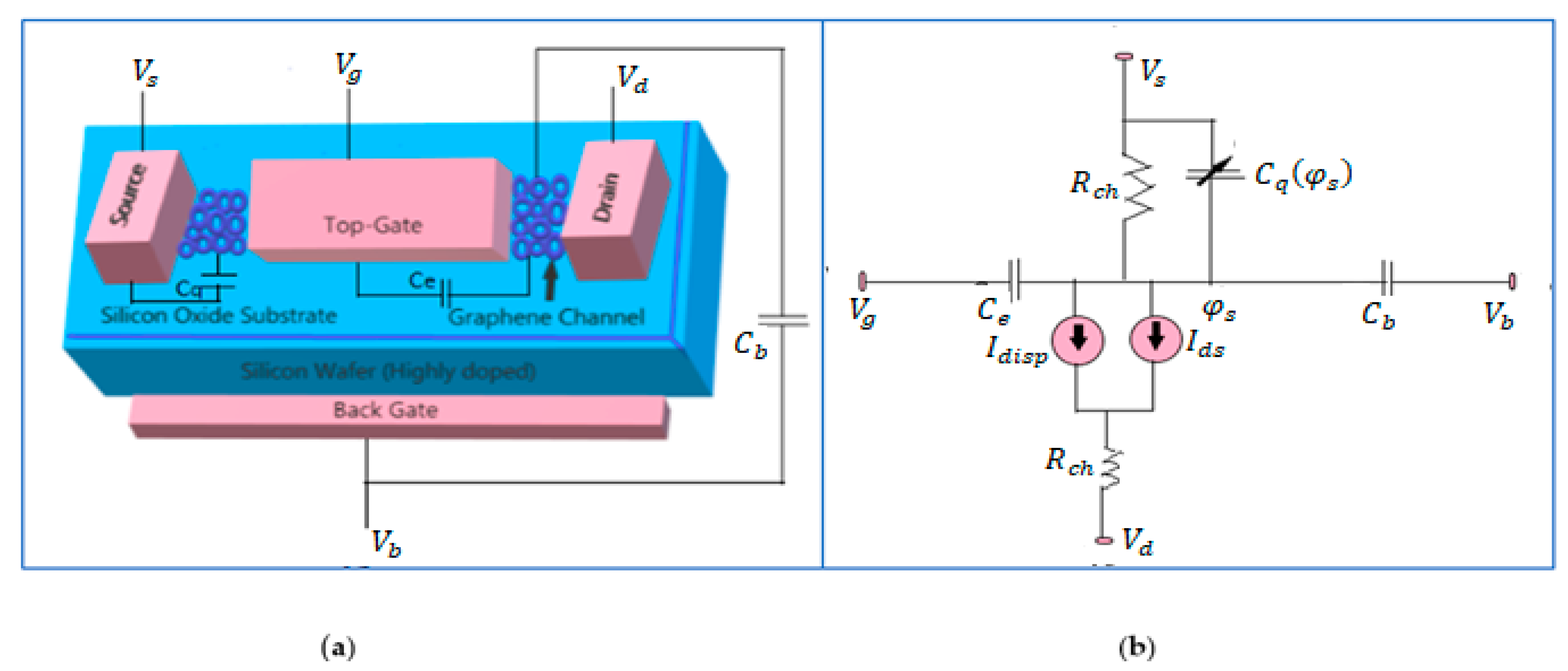
Figure 1a shows the physical structure of graphene FET in a three-dimensional pattern. Additionally, electrical equivalent circuit of GEFET is shown in Figure 1b. Firstly, the analytical expression for top gate capacitance (), back gate capacitance (), and threshold voltage () is shown for single-layer graphene channel. Next, electronic transport characteristics for hole and electron conduction was analyzed. Relationship between drain current () and drain-to-source voltage () was determined. Dependence of drain current () on gate voltages () was encountered. Characteristics of channel transconductance () and transit frequency () were mentioned. Finally, bilayer validation for different dielectrics was plotted by the relationship between threshold voltage and back-gate-to-source voltage.
2.1. Calculation of Threshold Voltage and Surface Potential for Single-Layer Graphene FET
The Dirac point is the crossing point of the linear energy dispersion. Because of two sublattices of graphene, there exist two symmetric Dirac points, −K and +K. These are the transitions between the valence band and conduction band. Quantum capacitance can be defined as the variation of electrical charge q with respect to the variation of potential. Variable quantum capacitance in relation to surface potential can be written as [26], where is the potential change between the graphene channel and the source voltage, ; q is the electrical charge, is the Fermi velocity [27], and ħ is the reduced Planck’s constant. Quantum capacitance depends upon the charge density, and for minimum carrier density the formula is [20]
We considered capacitance between the top gate and the graphene channel as and is the capacitance between the back gate and the channel. The top gate capacitance due to the effect of top gate potential can be written as
and the back gate capacitance due to the back gate potential can be expressed as
Applying capacitive voltage divider formula surface potential can be written as [20]
For top-gate-to-source voltage at Dirac point and back-gate-to-source voltage at Dirac point , the threshold voltage is
Hence, considering Equation (4), quantum capacitance can be stated as
This equation is related to Fermi level Here, Fermi level can be written as and represent electron conduction and hole conduction channel, respectively.
2.2. Surface Potential Calculation for Bilayer Graphene FET
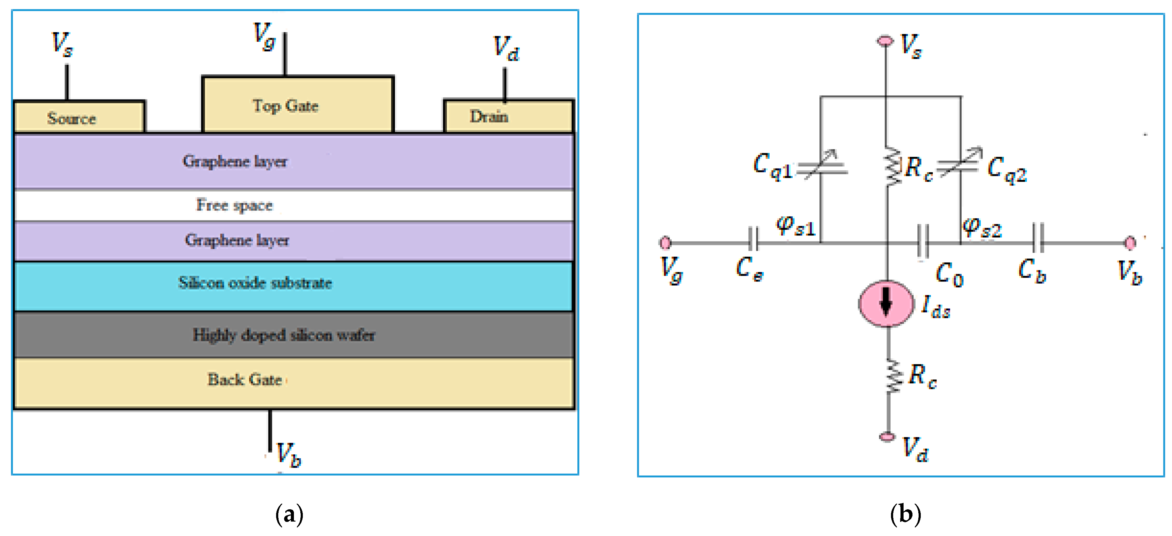
Compared to single-layer structure in bilayer GFET, there is an interlayer capacitance between two quantum capacitances, as shown in Figure 2a,b.
According to the equivalent capacitance model of bilayer graphene FET from Figure 1b, surface potential for the first and second layer is [21]
Surface potential of the first layer indicates the position of Fermi level according to its output. Positive value and negative value imply Fermi level is in the conduction band and valence band, respectively. It locates in the charge neutrality point when output is zero. When surface potential is zero, gate-to-source voltage can be considered as threshold voltage and it can be written as =−. This theory exhibits similarity with the Fermi level shift in the suspended part from Laitinen equation [28].
2.3. Relationship between Drain Current and Voltages
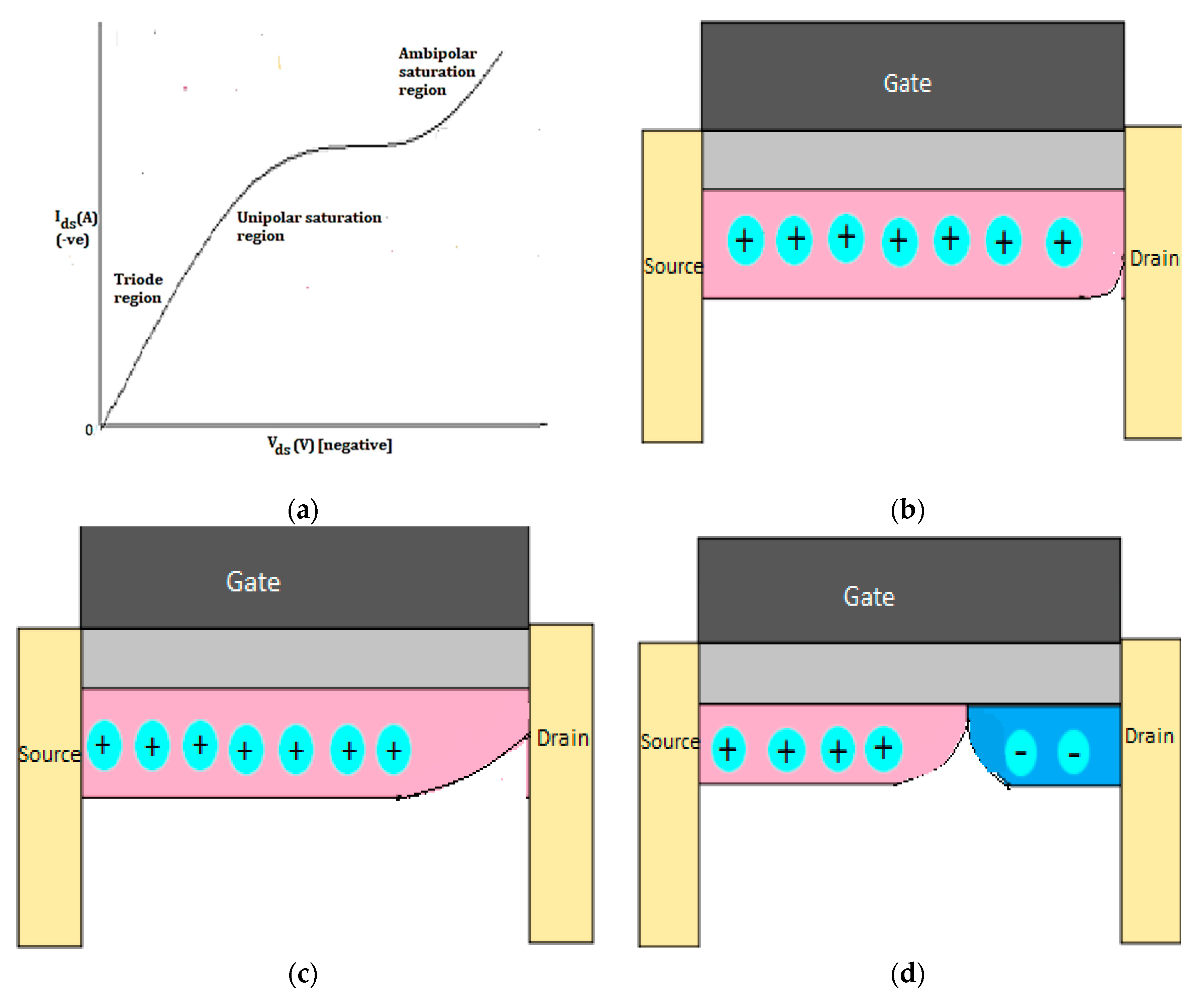
Figure 3a shows the I-V curve of graphene film. The characteristics can be explained by segmenting it into three sections: the triode region, unipolar saturation region, and ambipolar saturation region. Charge carriers in the first two areas are unipolar (electrons or holes). The curve got squeezed at the drain terminal in the unipolar saturation region. Ambipolar section demonstrates both of the charge carriers (electrons and holes).
In the triode region, the charge carriers (either holes or electrons) between the source and the drain ends generate drain current [29,30]:
Here, is the width of the channel and is the drift velocity of the charge carrier. The charge carrier experiences a saturation velocity due to the effective electrical field between drain and source terminal. The drift velocity is formulated by [31]. Here, E is the electric field between the drain and the source terminal, µ is the mobility of the charge carrier, and saturation velocity is = where is the critical electric field. In the triode region of the transistor, drain current is directly proportional to drain–source voltage. The electrical voltage in the graphene channel can be written as and where is a series resistance at both drain and source ends, respectively, and L is the active length of the graphene channel. The drain current of the triode region can be obtained by applying the Boltzmann equation and integrating Equation (9) along channel length [32]:
where and . Here and can be found from Equation (5). One can derive a simplified drain current Equation (11) by substituting the above values in Equation (10):
where and .
For the unipolar saturation region, there is a minimum charge density point at the terminal of drain that produces a saturation region. At this point, change of current with respect to voltage is . At the beginning of the first saturation region, the drain-to-source voltage can be defined as
After substituting the value of this saturation voltage into drain current in Equation (11), the derivation yields
From Figure 3a we can depict that the saturation current which maintains a continual progression through this region. Graphene channel experiences a saturation voltage at the drain terminal but it may not introduce a charge neutrality point. Considering a direct continuation of charge between and , the depletion charge between these two voltages will be , where. To eliminate this depletion charge,, generates and indicates the finishing point of unipolar saturation region. At this moment, the charge between and is , which is similar to . Therefore, the secondary terminal saturation voltage in this region can be formulated as [20]. This point introduces a pinch-off region at the drain terminal, which indicates a minimum carrier density. Pinch-off region in the drain current is shown by Figure 3a,c.
From Figure 3b,c, it can be understood that triode and unipolar saturation regions exhibit unipolar charge carrier and that is by holes. Afterwards, an ambipolar region is introduced, where carrier transportation is both by holes and electrons. Further increase in drain-to-source voltage pushes the minimum carrier density point at the pinch-off region toward the inside, i.e., this squeezed portion comes close to the source end. In this way, electrons get scope to enter into the channel, as indicated in Figure 3d. Therefore, this region becomes a complete package of holes and electrons running from source and drain terminals, respectively. For the mobility of the electrons there is no drained region between pinch-off and drain terminal. This phenomenon ultimately reaches to a concept that explains the zero bandgap theory in two-dimensional bilayer graphene. The voltage and charge accumulated at the drain terminal is and , respectively. Additional charge that is introduced can be formulated as where and is the mobility of the opposite charge carriers. We can derive by applying integration on using [26]. As a result, the saturation displacement current is obtained
The saturation drain current at the unipolar saturation region due to depletion charge and displacement current from additional charges in ambipolar region result in a total current flow in the graphene channel, .
2.4. Calculation of Transconductance and Transit Frequency
The transconductance is a significant parameter for understanding the RF performance of GFET. Generally, high is desirable for high intrinsic gain and cutoff frequency. The can be extracted from transfer characteristics of GFET, which means change of drain current with a small change of gate voltage as Where constant. Here, the can be calculated by the approximation that the drain-to-source resistance is zero. By taking differentiation of saturation current with respect to voltage gate voltage, transconductance at saturation can be obtained as:
Intrinsic cutoff frequency is another important parameter to characterize the GFET RF performance. The intrinsic cutoff frequency of a transistor is determined by charge carrier transit time across the channel length (L gate). The intrinsic cutoff frequency [33] can be deduced by:
3. Results and Discussion
Performance of the graphene film as a flexible GFET was calibrated and analyzed. The surface potential and quantum capacitance as a function of gate voltage were investigated. The output and transfer characteristics were obtained. The contribution of high transit frequency as a function of gate voltage and channel length dependence was also found and discussed. Moreover, transconductance and threshold voltage dependence on gate voltages was clarified. The surface potential was expressed as a function of the gate-source voltage and simulated the quantum capacitance as a function of surface potential by using the following data: Top-gate dielectric constant 16.0 and back-gate dielectric constant 3.9 were considered. Herein, the device threshold voltage was considered. The top gate source voltage at the Dirac point and back gate source voltage at the Dirac point were taken as 1.45 V and 2.7 V, respectively. Back gate oxide layer thickness was taken as 285 nm. Channel series resistance was taken as 850 Ω. Here, surface mobility and mobility of alternative carriers were 700 and 120, respectively. The channel length and channel width were assumed as 440 nm and 1 µm, respectively. The top-gate oxide-layer thickness was taken as 15 nm. The critical electrical field was considered as 4.5 KV/cm.
3.1. Top-Gate-to-Source Voltage Dependence on Quantum Capacitance and Surface Potential
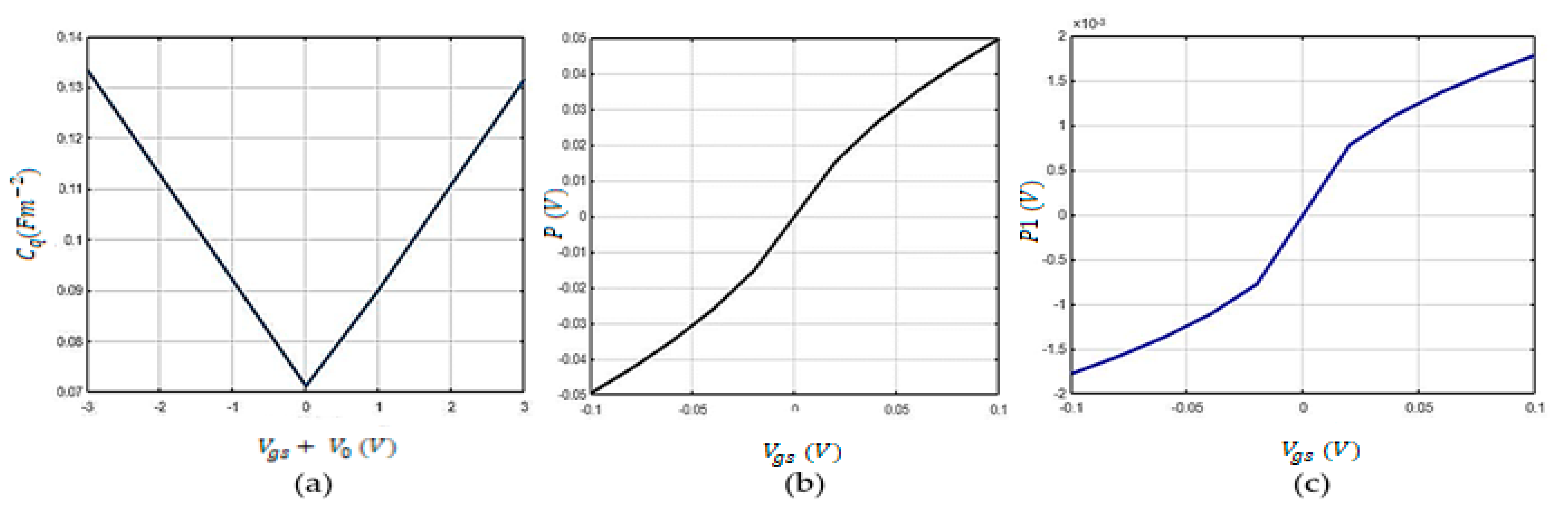
The graphical presentation of gate-to-source voltage with quantum capacitance and surface potential is shown in Figure 4. It was found that a V-shaped curve where the maximum value of quantum capacitance occurred at 0.13 at −3 V and at 3 V, respectively. The minimum quantum capacitance was obtained as 0.01 at V = 0. The top-gate and back-gate dielectric constants were taken as 16.0 and 3.9, respectively. Increase of dielectric constant meant increase in the charge accumulation in the channel. Therefore, the capacitance was automatically increased for a particular fractional change in potential. Increase in charge carrier concentration meant high on-current as well as high off-current but an increase in on/off ratio.
According to the calculation of the surface potential in Section 2, it was dependent on the gate voltage, and the plot in Figure 4b confirms it. Actually, the surface potential p (v) in Figure 4b is the potential difference between the channel and the source terminal. For each value of quantum capacitance, surface potential vs. gate voltage was obtained self-consistently. At surface potential was also zero. At minimum gate voltage, surface potential was taken. At maximum gate voltage, surface potential was taken, i.e., characteristics were also anti-symmetrical. Fermi level is related to surface potential by the relation where is Fermi level, q is the quantum capacitance, and P is the surface potential. Positive value of surface potential indicates that the Fermi level is in the conduction band, negative value indicates that the Fermi level is in the valence band, and a zero value indicates a charge neutrality point.
3.2. Relationship between Drain Current and Voltages
The curve in which the relationship between drain current and drain voltage has been represented gives the output response of the device, as illustrated in Section 2 theoretically in Figure 4a, which shows the output characteristics of this GFET for electron conduction. Through application of a positive gate voltage and a positive drain voltage, it provides current flow only when is higher than the device threshold voltage.
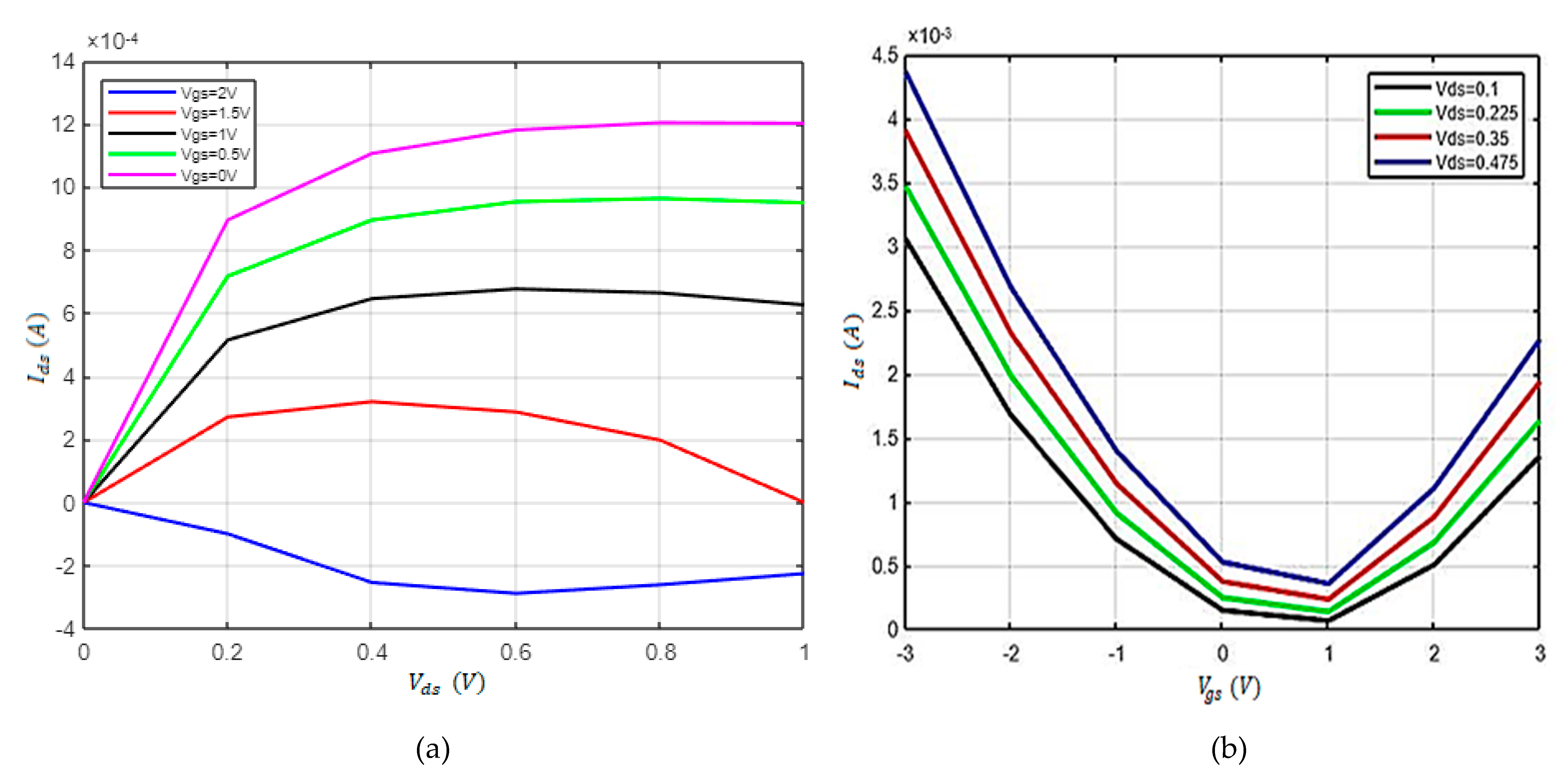
The behavior for electron conduction is shown in Figure 5a where top-gate voltages = 0 V, 0.5 V, 1 V, 1.5 V and 2 V, = +40 V, = 850 Ω, µ = 700, = 4.5 KV/cm, and = 120 are estimated, respectively. The output characteristics showed a linear region, a weak saturation region, and, in some cases, a second linear region. The value of is 0.00121 A at saturation region. Good current saturation and disappearance of second linear region were observed on output characteristics for higher . The maximum on-state current of 1.21 mA was obtained for .
In Figure 5b, the drain current shows a V-shaped curve with respect to the top-gate- to-source voltage. It represents the transfer characteristics of a particular device. The characteristics were plotted for a transistor with = +40 V, = 850 Ω, µ = 700, and = 120 with a of 0.1 V, 0.225 V, 0.35 V, and 0.475 V for electron conduction. = −3 V, −2 V, −2 V, 0 V, 1 V, 2 V, and 3 V were taken, respectively. For different , where ambipolar conduction was clearly distinguished by a Dirac point, there was an asymmetry in p-type and n-type conduction in transfer characteristics. The Dirac point represents the vanishing point of density of states but there is a minimum conductance unlike other semiconductors. The position of Dirac point depends on several factors: the difference between the work functions of the gate material and graphene, the type and density of the charges at the top and bottom of the interfaces of the channel, and the amount of doping of the graphene. The value of residual charge at the Dirac point increases with as the channel potential depends not only on the but also on the.
3.3. Characteristics of Transconductance and Transit Frequency
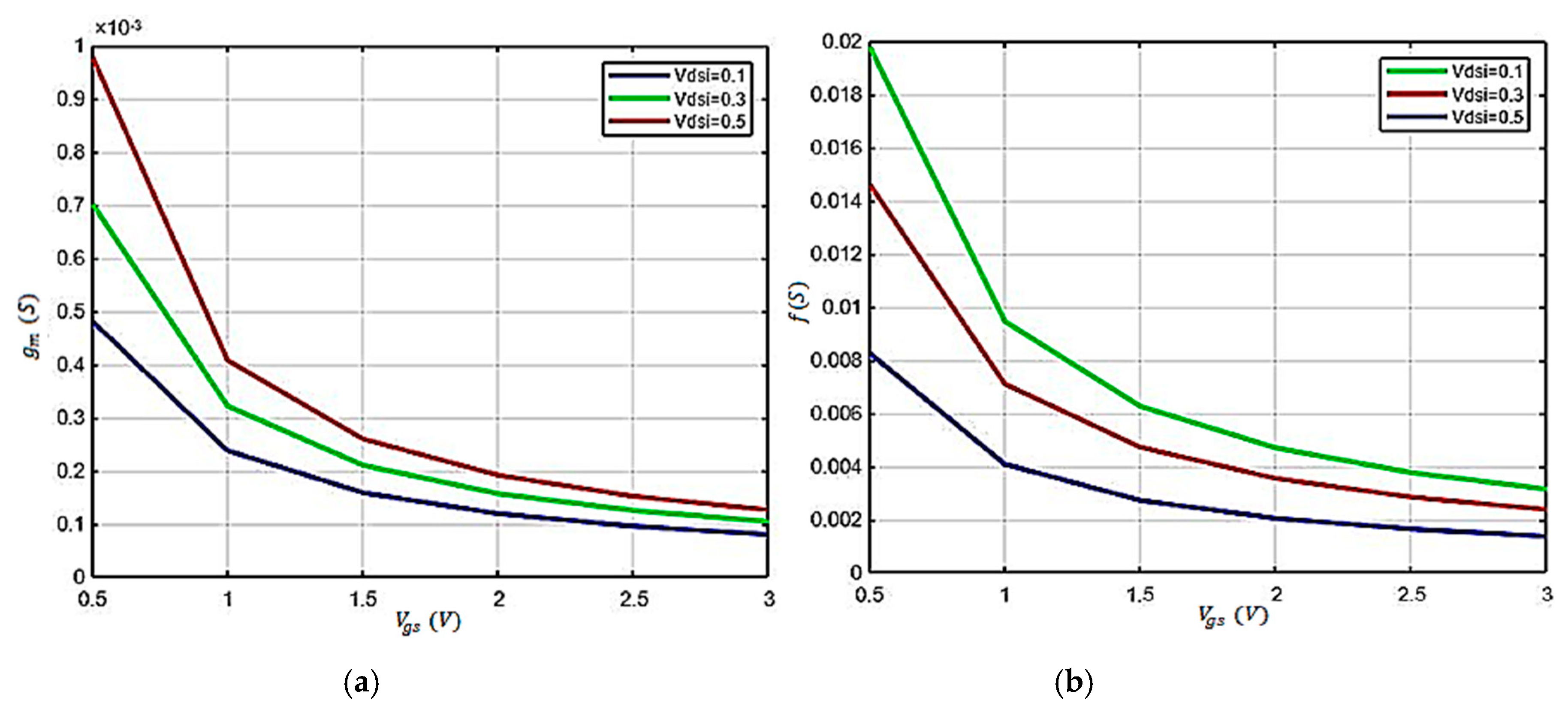
The output conductance is the change in the drain current with a small change in the gate source voltage while maintaining the drain source voltage constant. In Figure 6a, is shown for a range of with = 40 V. Length and width of graphene channel was taken as 440 nm and 1 µm, respectively. Here, were considered. It is interesting to notice that output characteristics displayed a linear region for low voltage bias and a saturation region for high voltage bias. The dropped substantially at large biasing voltage, mainly due to the effect of . As per the equation presented in Section 2.3, there is an inverse relationship between transconductance and gate source voltage. Therefore, the best performance was actually achieved at low effective gate-to-source overdrive voltage , where . The Figure 6b shows the estimation of transit frequency at which the current gain of the device drops to one, and it is a measure of its high-speed and bandwidth capabilities. Here,
3.4. Threshold Voltage Dependence on Back-Gate-to-Source Voltage
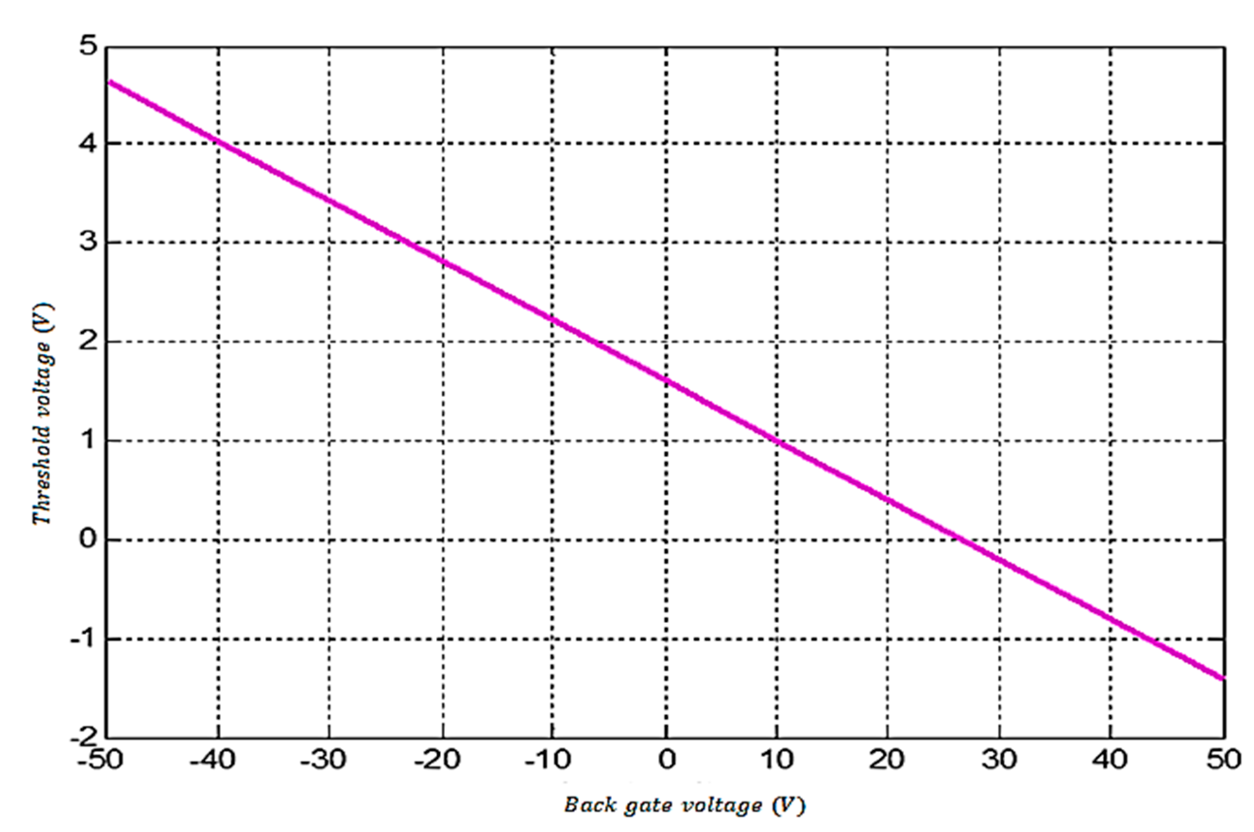
In the case of the plot, as shown in Figure 7, was used as dielectric. For a given back gate voltage (), the threshold voltage (was dependent on the device capacitances. Model parameters used are estimated in Table 1. For the test case shown in Figure 6, a good fit against experimental data was attained with top gate capacitance and back gate capacitance , respectively. It was reported that the threshold voltage against was a straight line graph with the slope being the ratio of the gate capacitances, as illustrated in Section 2.
4. Proposed Capacitive Model of Multilayer Graphene FET
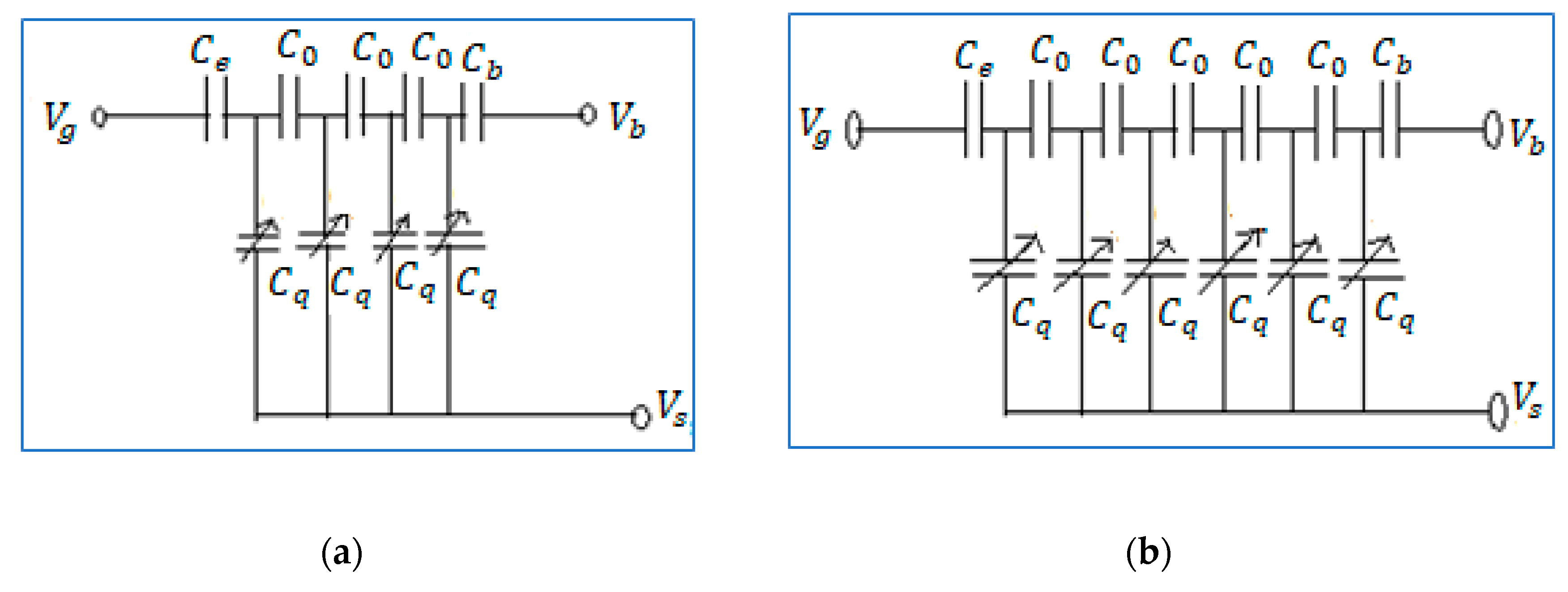
In Figure 8, four-layered and six-layered capacitive models are proposed. More extension of graphene channel can be done in a similar way. This is the equivalent demonstration of multilayer graphene FET. The layers are individually represented by quantum capacitance. There is an interlayer capacitance between the gaps of each of the channels. Further studies for multilayer channel can be done based on the formulae presented in Section 2 and simulating the properties using MATLAB.
5. Conclusions
This paper presented a theoretical model for single- and bilayer graphene channel. Later on, practical analysis of a dual-gate bilayer graphene FET was done utilizing MATLAB software. It considered the approximation of equality of mobility of electrons. Better output characteristics, transfer function, and transconductance behavior of GFET than FETs of other conventional semiconductors were obtained. The quantum capacitance as a function of top-gate-to-source voltage and surface potential with variation of gate bias was depicted. The minimum capacitance of 0.01 was obtained at the Dirac point where voltage is zero. When gate bias was negative, it gained negative value with a zero at zero gate bias. It was also found that when gate voltage was positive, it increased from zero value to source positive value. At minimum and maximum gate voltage, the surface potential was –0.05 V and +0.05 V, respectively. A set of output characteristics for different gate voltages was obtained. The drain current increased linearly then became saturated. The maximum 1.18 mA on state current was found. The transfer characteristics of the proposed model showed that, when gate voltage increased from a negative value, drain current reduced, at zero gate bias and over some voltages it became partially saturated, and then with the positive values’ output current tended to rise again. The transconductance estimation as a function of gate voltage for different drain-to-source voltages depicted proportional relationship; however, with the increase of gate voltage this value tended to fall. The transit frequency response as a function of gate voltage was represented whereas with the decrease of channel length the increment of transit frequency was obtained. The threshold voltage dependence on back gate source voltage for different dielectrics depicted that there was an inverse relationship between the two. Finally, equivalent capacitive model for multilayer graphene FET was proposed. The findings can be extended, including the following. (1) Extensive investigation can be done for multilayer graphene FET using MATLAB. (2) Contact resistance effect can be included for obtaining accurate performance. So this work can be extended for different contact metal stacks, metal alloys etc. (3) Buffer layer can be used to improve the device performance. Since phonon and surface roughness scattering reduces the mobility significantly, the buffer layer could make a good interface with reduced remote phonon scattering, which results in higher mobility.
Author Contributions
Conceptualization, S.H.; methodology, S.H.; software, M.A.P.M.; validation, A.Z.K. and M.A.P.M.; formal analysis, S.H.; investigation, S.H.; resources, M.A.P.M.; data curation, S.H.; writing—original draft preparation, S.H.; writing—review and editing, A.Z.K. and M.A.P.M.; visualization, S.H.; supervision, M.A.P.M.; project administration, M.A.P.M.; funding acquisition, A.Z.K. and M.A.P.M. All authors have read and agreed to the published version of the manuscript.
Funding
This research received no external funding.
Institutional Review Board Statement
Not applicable.
Informed Consent Statement
Not applicable.
Data Availability Statement
No additional data available.
Conflicts of Interest
The authors declare no conflict of interest.
References
- Iijima, S. Helical microtubules of graphitic carbon. Nature 1991, 354, 56–58. [Google Scholar] [CrossRef]
- Novoselov, K.S.; Geim, A.K.; Morozov, S.V.; Jiang, D.; Zhang, Y.; Dubonos, S.V.; Grigorieva, I.V.; Firsov, A.A. Electric Field Effect in Atomically Thin Carbon Films. Science 2004, 306, 666–669. [Google Scholar] [CrossRef] [PubMed] [Green Version]
- Kedzierski, J.; Hsu, P.; Healey, P.; Wyatt, P.; Keast, C.; Berger, C.; de Heer, W. Epitaxial Graphene transistors on SiC Substrates. IEEE Trans. Electron Devices 2008, 55, 2078–2085. [Google Scholar] [CrossRef] [Green Version]
- Han, M.Y.; Oezyilmaz, B.; Zhang, Y.; Kim, P. Energy Band-Gap Engineering of Graphene Nanoribbons. Phys. Rev. Lett. 2007, 98, 206805. [Google Scholar] [CrossRef] [Green Version]
- Meric, I.; Han, M.Y.; Young, A.F.; Oezyilmaz, B.; Kim, P.; Shepard, K.L. Current saturation in zero-bandgap, top-gated graphene transistors. Nat. Nanotech. 2008, 3, 654–659. [Google Scholar] [CrossRef]
- Kim, K.; Choi, J.-Y.; Kim, T.; Cho, S.-H.; Chung, H.-J. A role for graphene in silicon-based semiconductor devices. Nature 2011, 479, 338–344. [Google Scholar] [CrossRef]
- Lin, Y.-M.; Dimitrakopoulos, C.; Jenkins, K.A.; Farmer, D.B.; Chiu, H.-Y.; Grill, A.; Avouris, P. 100-GHz Transistors from Wafer-Scale Epitaxial Graphene. Science 2010, 327, 662. [Google Scholar] [CrossRef] [Green Version]
- Moon, J.S.; Curtis, D.; Hu, M.; Wong, D.; McGuire, C.; Campbell, P.M.; Jernigan, G.; Tedesco, J.L.; VanMill, B.; Myers-Ward, R.; et al. Stability Degradation in Bottom-gate Graphene Field-effect Transistors. IEEE Electron Device Lett. 2009, 30, 650. [Google Scholar] [CrossRef]
- Jenkins, K.A.; Lin, Y.-M.; Farmer, D.; Dimitrakopoulos, C.; Chiu, H.-Y.; Valdes-Garcia, A.; Avouris, P.; Grill, A. Graphene RF Transistor Performance. ECS Trans. 2020, 28, 3–13. [Google Scholar] [CrossRef] [Green Version]
- Liao, L.; Duan, X. Graphene for radio frequency electronics. Mater. Today 2012, 15, 328–338. [Google Scholar] [CrossRef]
- Novoselov, K.S.; Jiang, D.; Schedin, F.; Booth, T.J.; Khotkevich, V.V.; Morozov, S.V.; Geim, A.K. Two-dimensional atomic crystals. Proc. Natl. Acad. Sci. USA 2005, 102, 10451–10453. [Google Scholar] [CrossRef] [PubMed] [Green Version]
- Novoselov, K.S.; Geim, A.K.; Morozov, S.V.; Jiang, D.; Katsnelson, M.I.; Grigorieva, I.V.; Dubonos, S.V.; Firsov, A.A. Two-dimensional gas of massless Dirac fermions in graphene. Nature 2005, 438, 197–200. [Google Scholar] [CrossRef] [PubMed]
- Zhang, Y.; Tan, Y.-W.; Stormer, H.L.; Kim, P. Experimental observation of the quantum Hall effect and Berry’s phase in graphene. Nature 2005, 438, 201–204. [Google Scholar] [CrossRef] [Green Version]
- Bolotin, K.I.; Sikes, K.J.; Jiang, Z.; Klima, M.; Fudenberg, G.; Hone, J.; Kim, P.; Stormer, H.L. Ultrahigh electron mobility in suspended graphene. Solid State Commun. 2008, 146, 351–355. [Google Scholar] [CrossRef] [Green Version]
- Lee, S.; Jagannathan, B.; Narasimha, S.; Chou, A.; Zamdmer, N.; Johnson, J.; Williams, R.; Wagner, L.; Kim, J.; Plouchart, J.-O.; et al. Record RF performance of 45-nm SOI CMOS technology. In Proceedings of the 2007 IEEE International Electron Devices Meeting, Washington, DC, USA, 10–12 December 2007; pp. 568–571. [Google Scholar]
- Liao, L.; Bai, J.; Cheng, R.; Lin, Y.-C.; Jiang, S.; Qu, Y.; Huang, Y.; Duan, X. Sub-100 nm Channel Length Graphene Transistors. Nano Lett. 2010, 10, 3952–3956. [Google Scholar] [CrossRef] [PubMed] [Green Version]
- Adam, S.; Hwang, E.H.; Galitski, V.; Das Sarma, S. A self-consistent theory for graphene transport. Proc. Natl. Acad. Sci. USA 2007, 104, 18392–18397. [Google Scholar] [CrossRef] [PubMed] [Green Version]
- Robinson, J.A.; Labella, M.; Zhu, M.; Hollander, M.; Kasarda, R.; Hughes, Z.; Trumbull, K.; Cavalero, R.; Snyder, D. Contacting graphene. Appl. Phys. Lett. 2011, 98, 053103. [Google Scholar] [CrossRef]
- Nagashio, K.; Nishimura, T.; Kita, K.; Toriumi, A. Metal/graphene contact as a performance killer of ultra-high mobility graphene analysis of intrinsic mobility and contact resistance. In Proceedings of the 2009 IEEE International Electron Devices Meeting (IEDM), Baltimore, MD, USA, 7–9 December 2009; Volume 9, pp. 565–568. [Google Scholar]
- Umoh, I.J.; Kazmierski, T.J.; Al-Hashimi, B.M. A Dual-Gate Graphene FET Model for Circuit Simulation—SPICE Implementation. IEEE Trans. Nanotechnol. 2013, 12, 427–435. [Google Scholar] [CrossRef]
- Umoh, I.J.; Kazmierski, T.J.; Al-Hashimi, B.M. Multilayer Graphene FET Compact Circuit-Level Model with Temperature Effects. IEEE Trans. Nanotechnol. 2014, 13, 805–813. [Google Scholar] [CrossRef] [Green Version]
- Rodriguez, S.; Vaziri, S.; Smith, A.; Fregonese, S.; Östling, M.; Lemme, M.C.; Rusu, A. A Comprehensive Graphene FET Model for Circuit Design. IEEE Trans. Electron Devices 2014, 61, 1199–1206. [Google Scholar] [CrossRef]
- Cao, T.T.; Nguyen, V.C.; Nguyen, H.B.; Bui, H.T.; Vu, T.T.; Phan, N.H.; Phan, B.T.; Hoang, L.; Bayle, M.; Paillet, M.; et al. Fabrication of few-layer graphene film based field effect transistor and its application for trace-detection of herbicide atrazine. Adv. Nat. Sci. Nanosci. Nanotechnol. 2016, 7, 035007. [Google Scholar] [CrossRef]
- Krajewska, A.; Pasternak, I.; Sobon, G.; Sotor, J.; Przewloka, A.; Ciuk, T.; Sobieski, J.; Grzonka, J.; Abramski, K.M.; Strupinski, W. Fabrication and applications of multi-layer graphene stack on transparent polymer. Appl. Phys. Lett. 2017, 110, 041901. [Google Scholar] [CrossRef]
- Shen, X.; Wang, Z.; Wu, Y.; Liu, X.; He, Y.-B.; Kim, J.-K. Multilayer Graphene Enables Higher Efficiency in Improving Thermal Conductivities of Graphene/Epoxy Composites. Nano Lett. 2016, 16, 3585–3593. [Google Scholar] [CrossRef] [PubMed] [Green Version]
- Fang, T.; Konar, A.; Xing, H.; Jena, D. Carrier statistics and quantum capacitance of graphene sheets and ribbons. Appl. Phys. Lett. 2007, 91, 092109. [Google Scholar] [CrossRef] [Green Version]
- Das, A.; Pisana, S.; Chakraborty, B.; Piscanec, S.; Saha, S.K.; Waghmare, U.V.; Novoselov, K.S.; Krishnamurthy, H.R.; Geim, A.K.; Ferrari, A.C.; et al. Monitoring dopants by Raman scattering in an electrochemically top-gated graphene transistor. Nat. Nanotechnol. 2008, 3, 210–215. [Google Scholar] [CrossRef] [PubMed] [Green Version]
- Laitinen, A.; Paraoanu, G.S.; Oksanen, M.; Craciun, M.F.; Russo, S.; Sonin, E.; Hakonen, P. Contact doping, Klein tunneling, and asymmetry of shot noise in suspended graphene. Phys. Rev. B 2016, 93, 115413. [Google Scholar] [CrossRef] [Green Version]
- Brews, J. A charge-sheet model of the MOSFET. Solid-State Electron. 1978, 21, 345–355. [Google Scholar] [CrossRef]
- Gray, P.R.; Hurst, P.J.; Lewis, S.H.; Meyer, R.G. Analysis and Design of Analog Integrated Circuits, 5th ed.; Wiley: NewYork, NY, USA, 2010. [Google Scholar]
- Sze, S.M.; Ng, K.K. Physics of Semiconductor Devices; Wiley-Interscience: NewYork, NY, USA, 2007. [Google Scholar]
- Scott, B.W.; Leburton, J.-P. Modeling of the Output and Transfer Characteristics of Graphene Field-Effect Transistors. IEEE Trans. Nanotechnol. 2011, 10, 1113–1119. [Google Scholar] [CrossRef] [Green Version]
- Wallace, P.R. The Band Theory of Graphite. Phys. Rev. 2002, 71, 622–634. [Google Scholar] [CrossRef]
Figure 1.
Configuration of a dual-gate graphene field effect transistor. (a) The 3D structure of the transistor. (b) Electrical equivalent circuit.
Figure 1.
Configuration of a dual-gate graphene field effect transistor. (a) The 3D structure of the transistor. (b) Electrical equivalent circuit.

Figure 2.
Schematic demonstration of bilayer graphene field effect transistor. (a) Bilayer transistor layout, (b) equivalent model.
Figure 2.
Schematic demonstration of bilayer graphene field effect transistor. (a) Bilayer transistor layout, (b) equivalent model.

Figure 3.
Diagrammatic representation of the charge flow in graphene field effect transistor. (a) I-V curve of transistor. (b) Triode region: Flow of holes and a minimum charge density point started to form at the drain end. (c) Unipolar saturation region: There is a pinching at the drain terminal. (d) Ambipolar region: Graphene channel illustrating both holes’ and electrons’ transport.

Figure 4.
Graphical representation of gate-to-source voltage with quantum capacitance and surface potential as: (a) quantum capacitance as a function of top-gate-to-source voltage and (b) surface potential P (V) vs. top-gate-to-source voltage of a graphene field effect transistor (FET) from equation of surface potential [21]. (c) Surface potential P1 (V) vs. top-gate-to-source voltage (V) from Laitinen equation of Fermi level shift [28].

Figure 5.
Graphical representation of drain-to-source and gate-to-source voltages with drain current as: (a) output characteristics of GFET and (b) drain current versus top-gate voltage.
Figure 5.
Graphical representation of drain-to-source and gate-to-source voltages with drain current as: (a) output characteristics of GFET and (b) drain current versus top-gate voltage.

Figure 6.
Graphical representation of the drain transconductance and transit frequency. (a) Transconductance as a function of gate voltage of graphene field effect transistor (GFET). (b) Transit frequency as a function of gate-to-source voltage.
Figure 6.
Graphical representation of the drain transconductance and transit frequency. (a) Transconductance as a function of gate voltage of graphene field effect transistor (GFET). (b) Transit frequency as a function of gate-to-source voltage.

Figure 7.
Graphical representation of threshold voltage dependence on back-gate-to-source voltage using silicon dioxide as dielectric.
Figure 7.
Graphical representation of threshold voltage dependence on back-gate-to-source voltage using silicon dioxide as dielectric.

Figure 8.
Equivalent capacitance model: (a) graphene channel with four layers, (b) graphene channel with six layers.
Figure 8.
Equivalent capacitance model: (a) graphene channel with four layers, (b) graphene channel with six layers.


Table 1.
Model parameters for bilayer graphene field effect transistor (FET).
| Model Parameter | Test Value | Estimated Value |
|---|---|---|
| L (µm) | 1 | 440 |
| W (µm) | 2.1 | 1 |
| 15 | 15 | |
| 4.5 | 4.5 | |
| 16.0 | 16.0 | |
| 3.9 | 3.9 | |
| 1.45 | 1.45 | |
| 2.7 | 2.7 | |
| 600 | 700 | |
| 120 | 120 | |
| 850 | 850 | |
| +40 | +40 |
Publisher’s Note: MDPI stays neutral with regard to jurisdictional claims in published maps and institutional affiliations. |
© 2020 by the authors. Licensee MDPI, Basel, Switzerland. This article is an open access article distributed under the terms and conditions of the Creative Commons Attribution (CC BY) license (http://creativecommons.org/licenses/by/4.0/).
Share and Cite
MDPI and ACS Style
Hasan, S.; Kouzani, A.Z.; Mahmud, M.A.P. Equivalent Circuit Modeling of a Dual-Gate Graphene FET. Electronics 2021, 10, 63. https://doi.org/10.3390/electronics10010063
AMA Style
Hasan S, Kouzani AZ, Mahmud MAP. Equivalent Circuit Modeling of a Dual-Gate Graphene FET. Electronics. 2021; 10(1):63. https://doi.org/10.3390/electronics10010063
Chicago/Turabian StyleHasan, Saima, Abbas Z. Kouzani, and M A Parvez Mahmud. 2021. "Equivalent Circuit Modeling of a Dual-Gate Graphene FET" Electronics 10, no. 1: 63. https://doi.org/10.3390/electronics10010063
Note that from the first issue of 2016, this journal uses article numbers instead of page numbers. See further details here.