Article

Room-Temperature O3 Detection: Zero-Bias Sensors Based on ZnO Thin Films

1
DiaTHEMA Lab, Institute of Structure of Matter (CNR-ISM), U.O.S. Montelibretti, Via Salaria km 29.300, 00015 Monterotondo, Italy
2
FemtoLAB, Institute of Structure of Matter (CNR-ISM), U.O.S. Tito Scalo, Zona Industriale, 85050 Tito, Italy
3
EscaLab, Institute for the Study of Nanostructured Materials (CNR-ISMN), Montelibretti, Via Salaria km 29.300, 00015 Monterotondo, Italy
4
Dipartimento di Scienze e Tecnologie Chimiche, Università degli Studi di Roma Tor Vergata, Via della Ricerca Scientifica, 00133 Rome, Italy
*
Author to whom correspondence should be addressed.
Crystals 2024, 14(1), 90; https://doi.org/10.3390/cryst14010090
Submission received: 13 December 2023 / Revised: 10 January 2024 / Accepted: 15 January 2024 / Published: 18 January 2024

Abstract

:
ZnO thin films with a thickness of 300 nm were deposited on Si and Al2O3 substrates using an electron beam evaporation technique with the aim of testing them as low cost and low power consumption gas sensors for ozone (O3). Scanning electron microscopy and atomic force microscopy were used to characterize the film surface morphology and quantify the roughness and grain size, recognized as the primary parameters influencing the gas sensitivity due to their direct impact on the effective sensing area. The crystalline structure and elemental composition were studied through Raman spectroscopy and X-ray photoelectron spectroscopy. Gas tests were conducted at room temperature and zero-bias voltage to assess the sensitivity and response as a function of time of the films to O3 pollutant. The results indicate that the films deposited on Al2O3 exhibit promising characteristics, such as high sensitivity and a very short response time (<2 s) to the gas concentration. Additionally, it was observed that the films display pronounced degradation effects after a significant exposure to O3.

1. Introduction

The increasing demand for monitoring air pollution, particularly due to greenhouse gases like CO2, NO2, SO2, and O3 [1], is a current challenge for human health care and environmental application. According to the World Health Organization’s air quality guideline for ozone [2], it is recommended that daily exposure to ozone, ensuring sufficient protection of human health, should not exceed 100 μg/m3, approximately equivalent to 50 parts per billion (ppb), as a maximum 8-h mean concentration. Since people spend most of their time in environments such as residences, schools, and offices, it is crucial to pay attention to indoor ozone exposure. Despite average ozone concentration levels in these spaces ranging from 4 to 6 ppb [3], peak concentrations during the day could exceed the WHO reference values [3].
Nowadays, the development of advanced gas sensors is fundamental to real-time monitoring of the ozone concentration in indoor environments. This latest generation of solid-state gas sensors reflects a transition from bulk materials with good intrinsic properties to materials with size- and shape-dependent surface properties, including nanostructured materials, nanoparticles, and ultra-thin films [4,5,6,7,8]. Thin films offer functionalized surfaces suitable for a wide range of applications [9,10,11], by combining different parameters such as the thickness, the substrate employed, and the deposition method used. With an increased surface-to-volume ratio, nanostructured thin films exhibit good performance in terms of sensitivity, selectivity, and quick response time [12,13,14].
Furthermore, the reduced size of thin films enables low-cost production processes and easy integration into devices, allowing for constant remote monitoring, wireless data collection, and processing using plug-and-play IoT (Internet of Things) technologies [15,16].
Thin film gas sensors can be produced using metal oxide semiconductors (MOXs). MOX sensors based on SnO2, ZnO, CuO, and WO3 stand out for their excellent performance in terms of sensitivity, selectivity, response time, and recovery time. Moreover, these materials are cost-effective and readily available, ensuring low production costs. The ability to synthesize these materials in nanostructure form ensures the occurrence of the surface conductance effect, thereby allowing for a reduction in the working temperature compared to bulk sensors. Working at lower temperatures, especially at room temperature, offers several advantages. It guarantees greater stability of the device, enabling the maintenance of sensitivity properties for an extended period in normal environmental conditions of temperature and humidity [17,18,19,20,21].
When exposed to gas, MOXs exhibit a chemiresistor behavior, where the electronic properties change upon gas molecule adsorption, enabling the detection of harmful gases through variation in the electrical resistivity [22]. While MOX-based gas sensors exhibit very short response times, high operating temperatures (300–500 °C) are typically required to achieve optimal sensitivity conditions [5,22,23,24,25]. However, ZnO can operate at lower temperatures, and it has been demonstrated that ZnO thin films can maintain high sensitivity even at lower temperatures (<100 °C down to room temperature) by optimizing film parameters such as grain size and porosity [5,26,27,28,29,30,31,32].
The choice of the physical vapor deposition (PVD) technique during the growth phase, such as magnetron sputtering, pulsed laser deposition (PLD), and electron-beam deposition, allows for control of these parameters. Each PVD technique offers respective advantages: magnetron sputtering enables higher thickness control, which is useful for ultra-thin film deposition [33]; PLD, on the other hand, guarantees higher ZnO crystallinity [33]. However, a recent study has suggested that electron-beam deposition is the most suitable technique for gas sensor design, as it generates polycrystalline films with high surface areas [33]. Different deposition methods yield ZnO films with varying grain sizes. The porosity, indeed, can be induced by growing the film on a rough substrate. Therefore, as a direct consequence of enhancing the surface-to-bulk ratio, it has been demonstrated that gas sensors require a porous microstructure and that their sensitivity considerably increases as the grain size decreases [34,35].
Currently, ZnO-based sensors are recognized for their effective performance at room temperature, and they are primarily used for detecting reducing gases like H2, H2S, CO, and common solvents such as ethanol, methanol, and acetone, as outlined in the review [36]. However, in the context of ozone monitoring and oxidizing gases in general, devices developed in recent years, even if they show remarkable sensitivity (up to 35 ppb of ozone concentration), require operation at temperatures ranging from 200 °C to 400 °C [37,38,39]. This temperature demand poses a significant issue for the intended application in this research, which aims to continuously monitor ozone concentrations in indoor environments, such as schools and offices. Hence, this study aims to investigate the possibility of fabricating ZnO thin films for ozone sensing that are suitable to operate at room temperature and do not require the application of an external bias with good sensitivity. Achieving these working conditions would make the proposed devices a promising solution in terms of reduced maintenance times and costs and therefore demonstrate its applicability to daily environments such as schools and offices. To achieve this, the ZnO thin films were deposited by using electron beam deposition on Si and Al2O3 substrates and by optimizing the growth conditions. First, the substrate was selected by studying the morphology and surface roughness of the deposited ZnO thin films, using scanning electron microscopy and atomic force microscopy. Then, the structural and elemental analysis of the films were characterized by Raman and X-ray Photoelectron (XPS) spectroscopies, respectively.
The ZnO-based sensors were exposed to O3 gas for sensitivity testing. In addition to analyzing the variation of electrical properties, the effects of O3 gas exposure on the film surfaces were also studied to verify the induced effects onto the surface.

2. Materials and Methods

2.1. Films Deposition by Electron Beam Evaporation

Thin films of ZnO were deposited by electron beam deposition on silicon wafers and alumina substrates. The deposition was performed in a high vacuum chamber evacuated at a base pressure of ~1.0 × 10⁻⁶ mbar. The ZnO pellets (99.99% purity, Mateck Material-Technologie & Kristalle GmbH, Julich, Germany) were kept in a molybdenum crucible (Kurt J. Lesker Company GmbH, Dresden, Germany) and evaporated by an electron beam of 6.5 keV kinetic energy and 18 mA current, controlled through an electromagnetic lens system to homogenize the deposition process. During the deposition, the chamber pressure was maintained at a value of ~1.0 × 10⁻⁵ mbar. Those parameters led to a film of 300 nm thickness after 5 min of deposition (the deposited film thickness was verified using atomic force microscope profiles).
Due to the roughness of the alumina bare substrate, a thickness of 300 nm was chosen as the thinnest option, ensuring both total and homogeneous coverage of the substrate with ZnO. The choice of the deposition rate of 1 nm/s was made to have a fine control of the deposition process, since higher deposited rates provided uncontrolled kinetics and consequently a worst quality of the thin film properties.

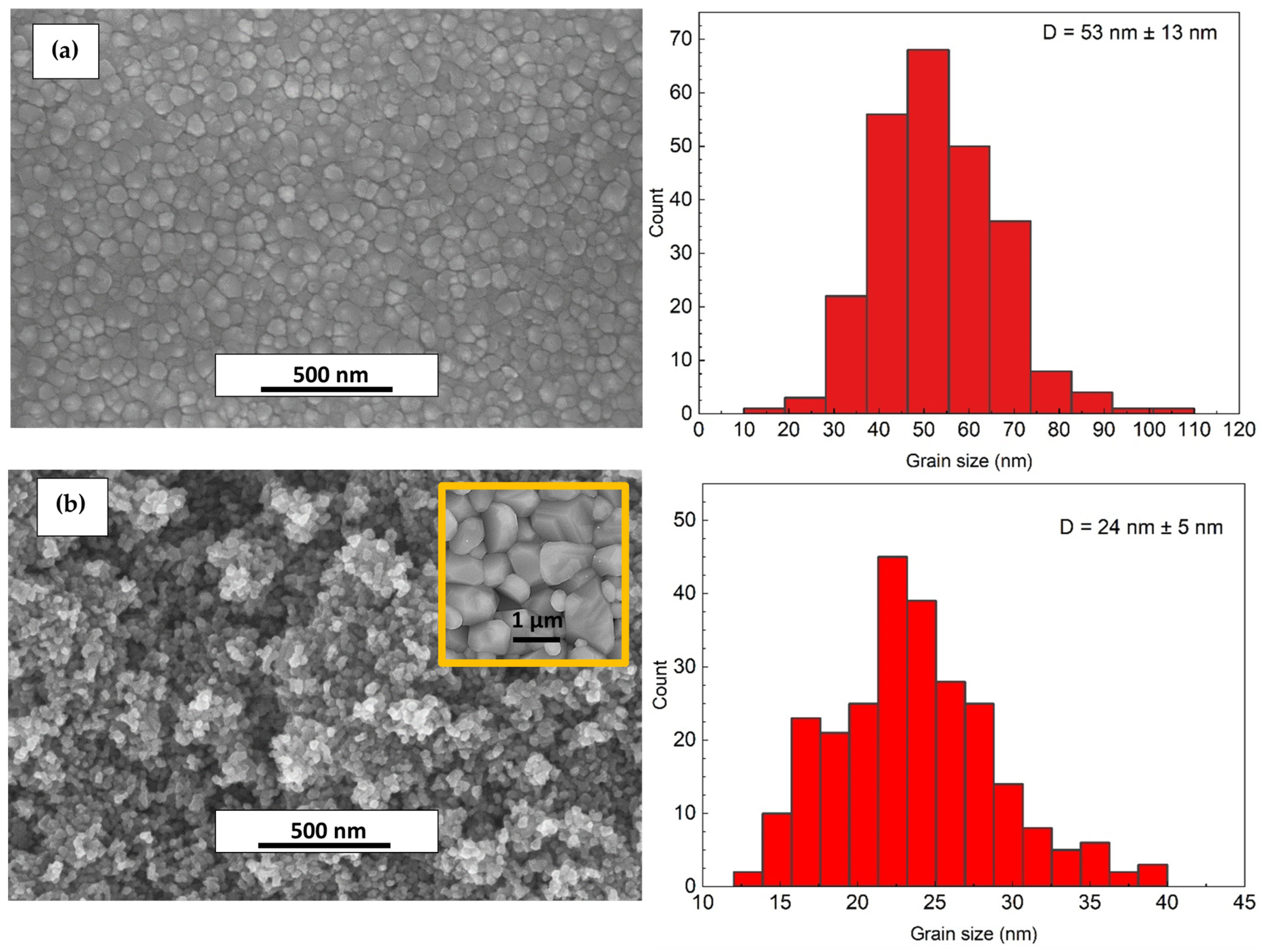
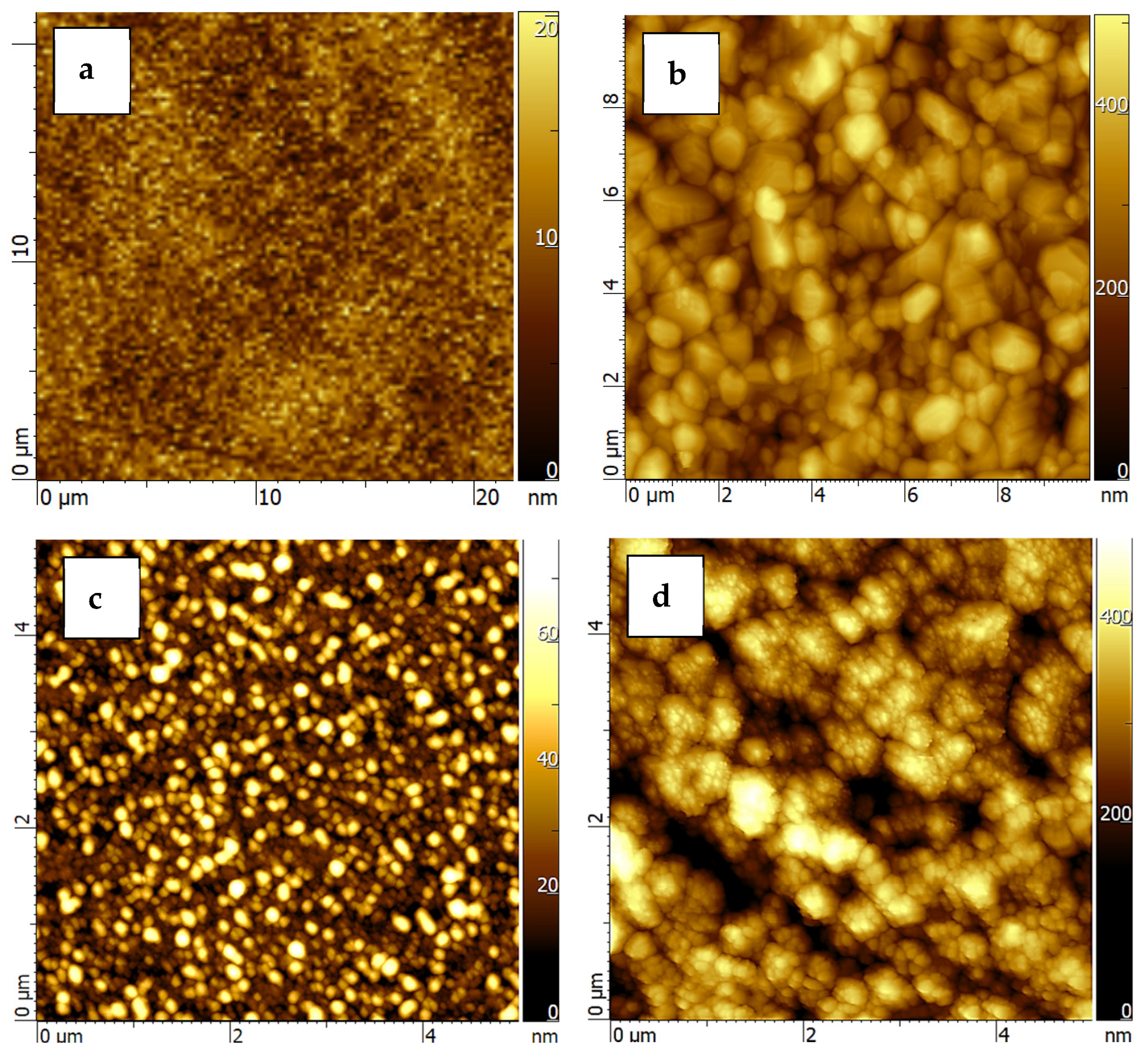
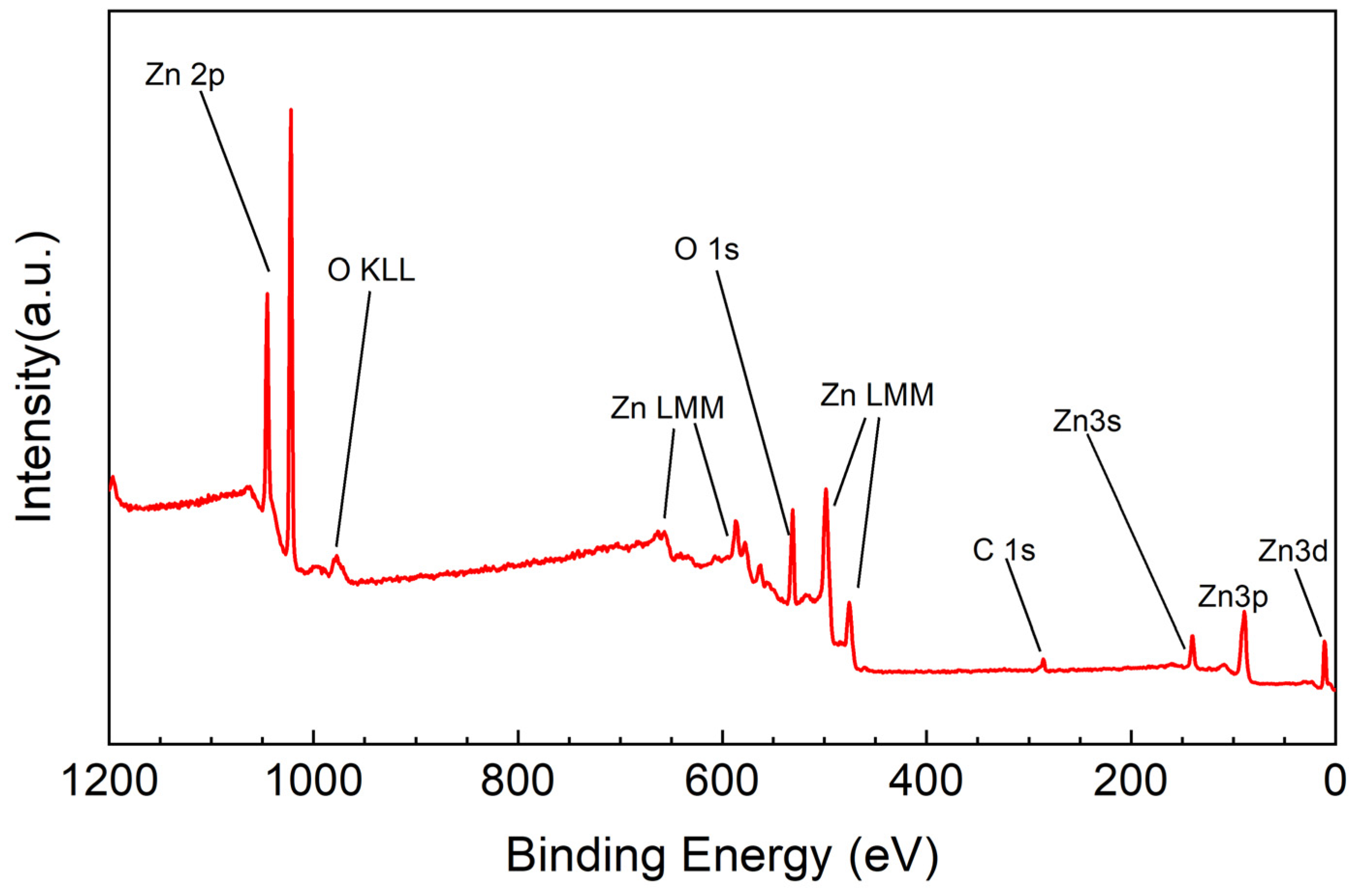
2.2. Structure and Morphology Characterization
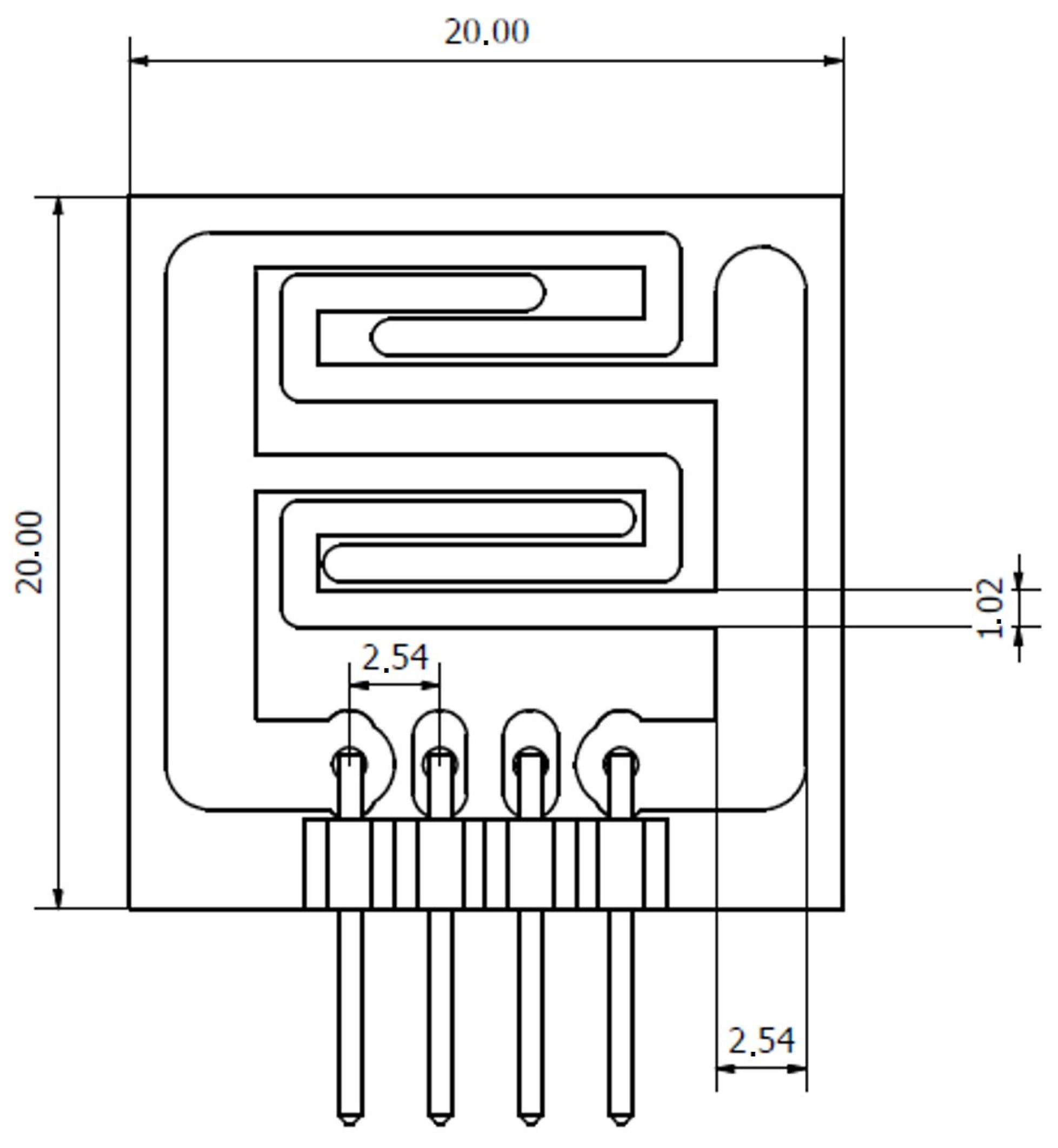
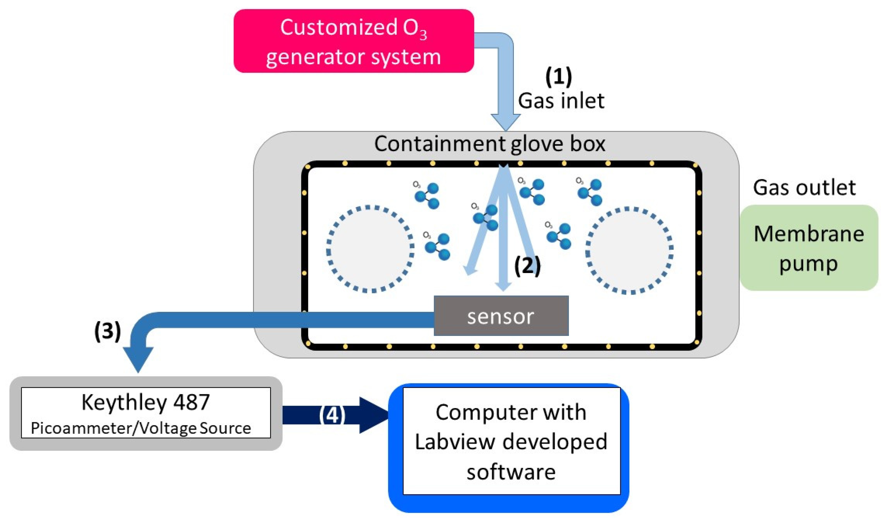
The morphology of the ZnO thin films has been investigated by Field-Emission Gun Scanning Electron Microscopy (FEG-SEM- Zeiss Leo Supra 35, Germany) and by Atomic Force Microscopy (AFM) carried out with use of an OmegaScope platform (HORIBA Ltd., Kyoto, Japan). AFM imaging was performed in tapping mode, setting the operational amplitude at 60 nm, and using a silicon pyramidal tip (MikroMasch HQ:NSC14/Al BS; Wetzlar, Germany) with a characteristic radius of ~8 nm. The resonance frequency was of 137 kHz. The scan rate was fixed at 0.6 Hz. All the AFM data were acquired, filtered, and analyzed using the AIST-NT.v3.5.160 SPM control software. Raman measurements were carried out by using a Horiba Scientific LabRam HR Evolution confocal spectrometer equipped with a 100 mW Oxxius (λexc = 532 nm) and 17 mW He-Ne (λexc = 633 nm) laser sources and a computerized XY-table, an electron-multiplier CCD detector, an Olympus U5RE2 microscope with a 100× objective (laser spot on the sample surface 0.7 μm) with a numerical aperture (NA) of 0.9, and a grating with 1800 grooves/mm. All Raman spectra were recorded in backscattering geometry focusing 10% of the laser sources power at the sample, and twenty spectra with an accumulation time of 10 s were averaged. Samples were measured before and after the gas exposure. XPS enabled the investigation of the composition of the ZnO films, and it was carried out by using a spectrometer ESCALAB 250 Xi (Thermo Fisher Scientific Ltd., East Grinstead, East Grinstead, UK), equipped with a monochromatic Al Kαsource (hν = 1486.6 eV) and a hemispherical analyzer with six-channeltron as the detection system. The XPS characterizations were performed in an ultra-high vacuum chamber at a base pressure of about 1 × 10⁻⁹ mbar. The binding energy (BE) scale was calibrated by positioning the C 1s adventitious carbon peak at BE = 285.0 eV with an accuracy of ±0.1 eV.

2.3. Gas Sensing

The ozone sensitivity tests were conducted only on the device comprising a thin film of ZnO (the receptor part of the sensor) deposited on an alumina (thickness: 1 mm) printed-circuit board (PCB) produced by CERcuits BV (Geel, Belgium) based on the specific design shown in Figure 1. This substrate was chosen for its suitability in microelectronics applications due to its good thermal conductivity, mechanical resistance, low dielectric constant, and dielectric loss.
To transduce the surface phenomena of film–ozone interaction, the substrates were equipped with two copper (Cu, 35 µm) electrodes. The inter-electrode gap at the minimum point between the two electrodes is 10 µm. A dedicated connector was soldered directly to these contacts, allowing for a convenient push-and-pull connection of the electrical contacts to the signal conditioner.
The gas sensor tests were performed using a commercial glove box (Cole-Parmer Instrument Company, LLC, UK) with a volume of about 0.25 m3, suitable to keep the gas concentration confined. Thanks to a customized ozone generator system (IONVAC Process srl, Pomezia, Italy), it was possible to regulate the flow of O3 in the chamber, which is evacuated by a membrane pump (pressure of ~10−1 mbar) to assure stable conditions and fast removal of ozone. The current measurements were carried out by connecting the sensor to an electrometer (Keithley 487 Picoammeter/Voltage Source), recording the data in an automated way through the management of the signals with the GPIB protocol and a software specifically developed with the LabVIEW (National Instruments, Austin, TX, USA) language. The measurements were carried out by observing the measured electrical current at zero-bias voltage in response to different pollutant concentrations inside the glove box. The experimental setup of the gas-sensing measurements is shown in Figure 2.

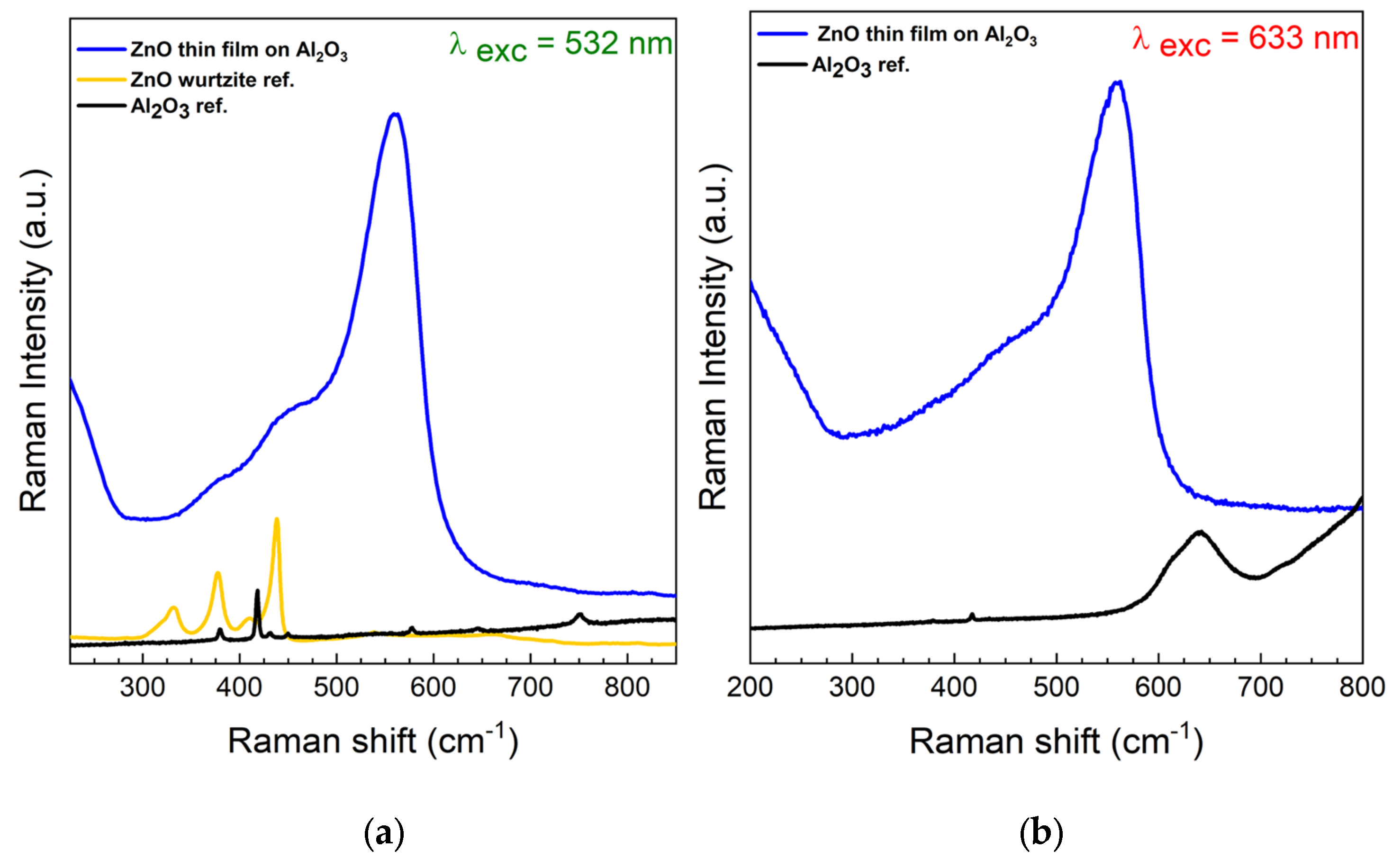
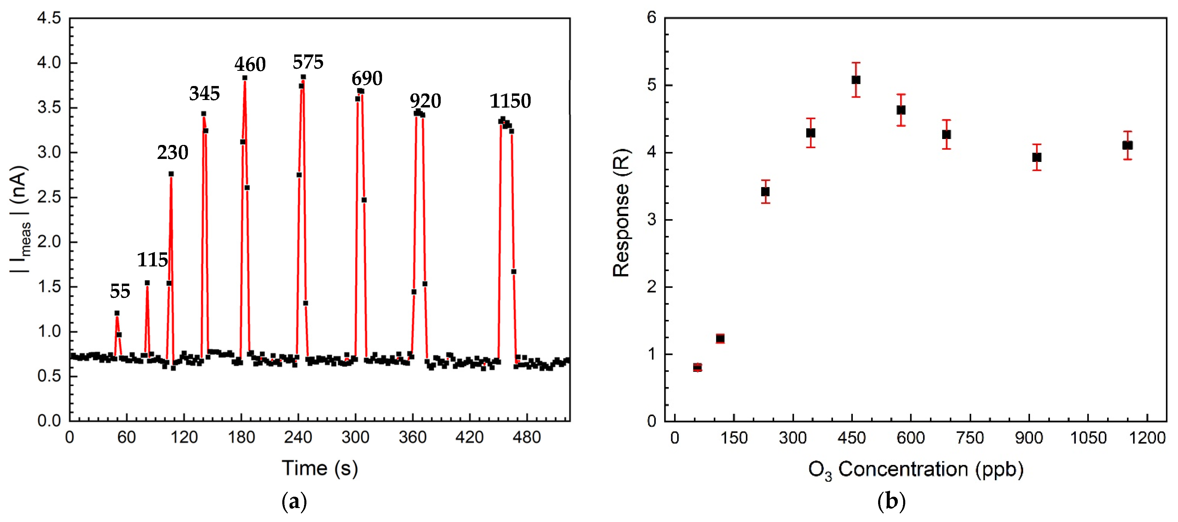
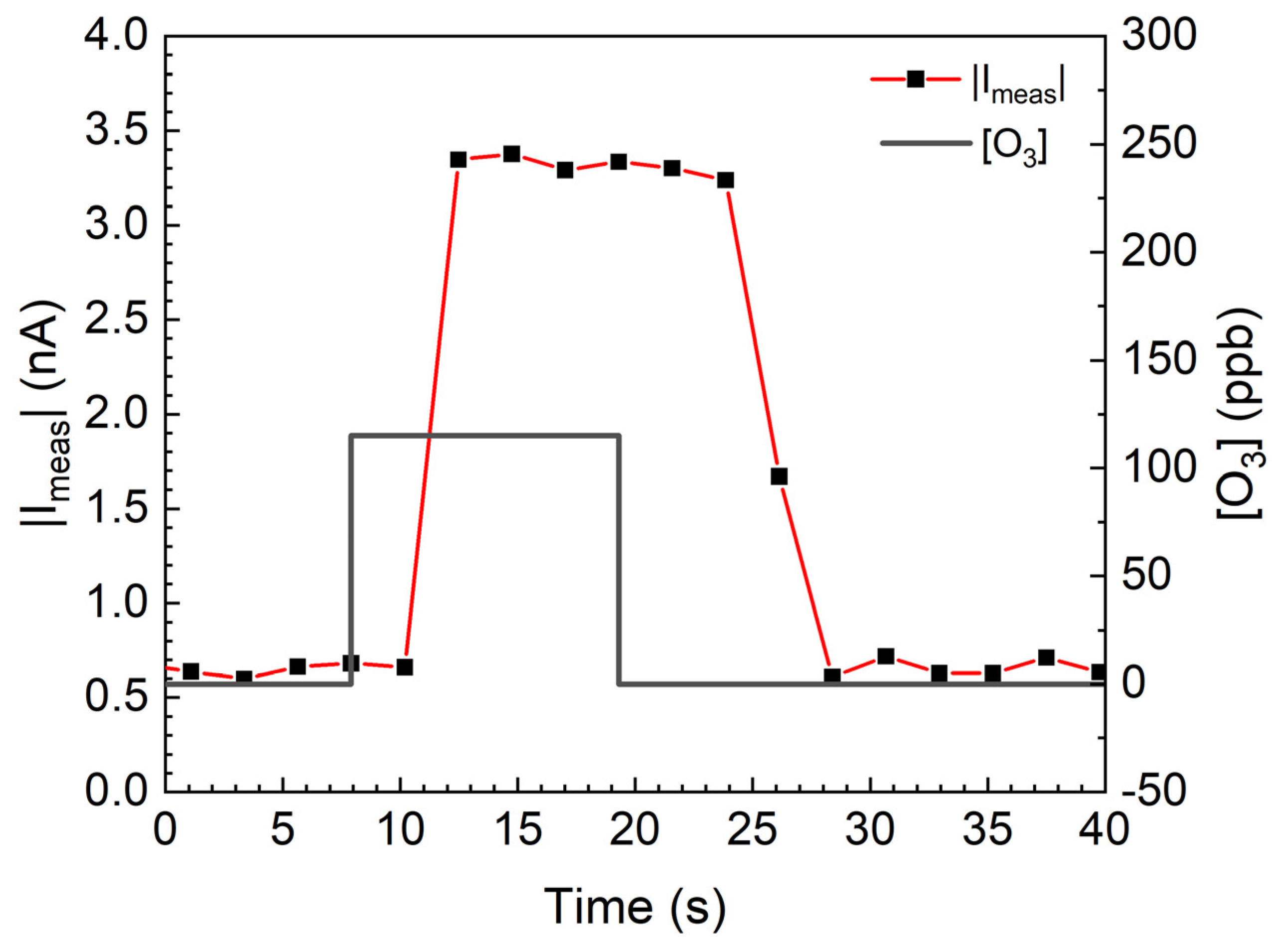
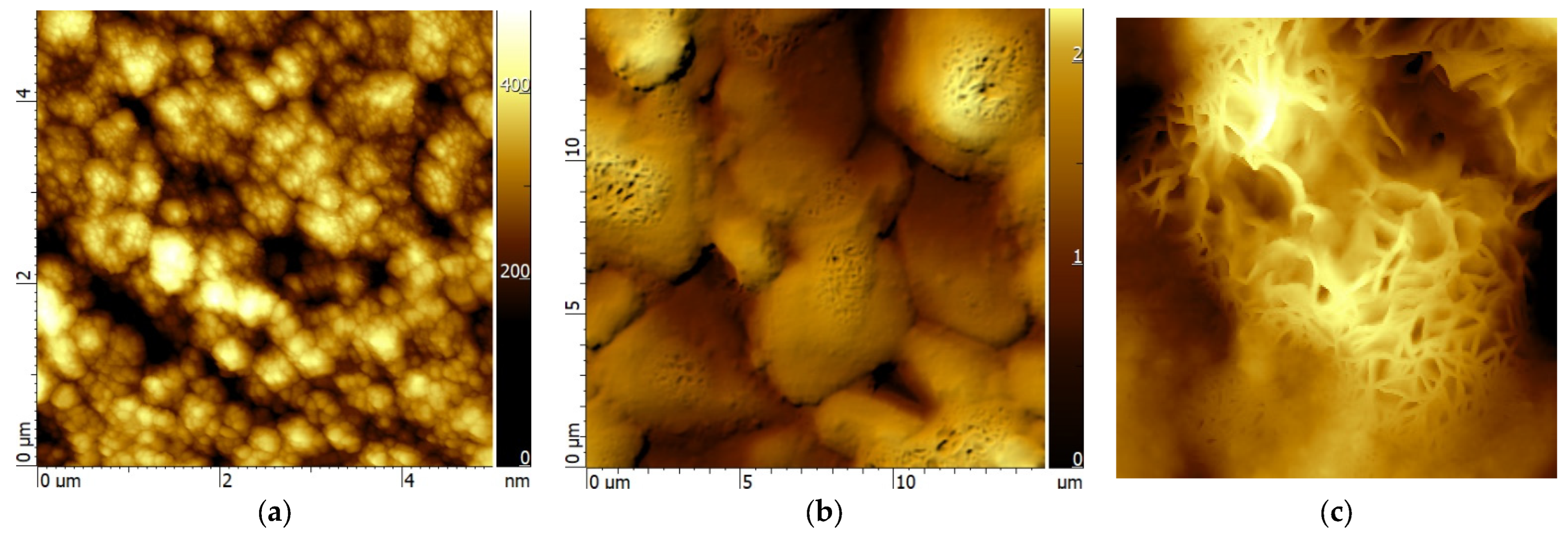
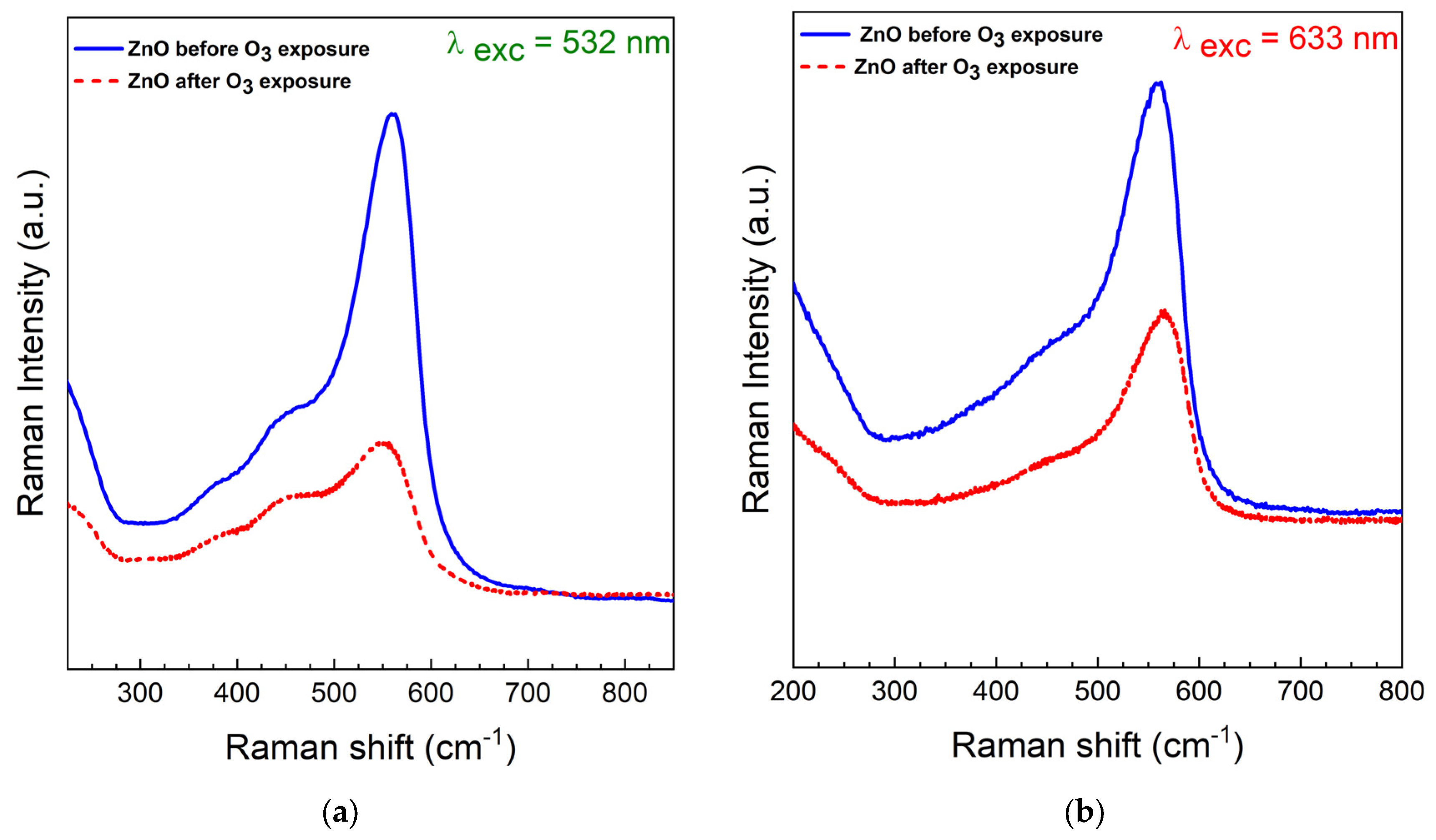
3. Results and Discussion

The ZnO thin films were deposited on the Si and alumina substrates by applying the declared deposition parameters to obtain homogenous and continuous thin films. To achieve this, it was found that the best conditions were able to maintain a deposition rate of 1 nm/s and were able to fix a thickness of 300 nm. Figure 3 illustrates the morphological differences between the films grown on Si (Figure 3a) and on alumina (Figure 3b) under the same conditions. The film deposited on Si appears smoother compared to the film grown on alumina. The average grain size was found to be 53 ± 13 nm for the Si-deposited film and 24 ± 5 nm for the alumina-deposited film.
Furthermore, the atomic force microscopy (AFM) analysis, as shown in Figure 4, confirmed the smoother surface of the film deposited on Si compared to the film grown on alumina (the bare substrates are shown in Figure 4a,b). The roughness parameters Ra and RRMS (i.e., Ra = the arithmetic average of the absolute values of the profile height deviations from the mean line, and RRMS = the root mean square average of the profile height deviations from the mean line) of the films were estimated using Aist.v3.5.160 software, analyzing images of an approximately 25 µm2 area with a lateral resolution of 500 × 500 pixels (Figure 4c,d). The results of the roughness analysis are summarized in Table 1.
It was found that the morphology of the ZnO films strongly depends on the substrate, with a different porosity and grain size that play a significant role in the film properties. Since a higher effective area obtained by the small grain size and high roughness is required to obtain better sensor performance [34,35,40], the morphological analysis led to the selection of alumina as the preferred substrate for growing the films to be used in the gas sensitivity tests.
The XPS measurements were performed to analyze the chemical composition of the most promising ZnO film. The C1s spectrum revealed the presence of contaminants, including adventitious carbon (C1) at a binding energy (BE) of 285.0 eV and carboxyl groups (C2) at a BE of 288.2 eV, due to exposure to air (XPS survey spectrum is shown in Figure 5). A 30 s-duration ion sputtering process with Ar+ at 2 keV effectively removed all contaminants from the film surface, as shown in Table 2. The XPS analysis confirmed the presence of stoichiometric ZnO films, with a slight excess of Zn observed after Ar+ cleaning due to the preferential sputtering effect described in the literature [41,42].
Raman spectroscopy provided additional information compared to XPS revealing the Al2O3 interface. Figure 6a shows the normalized Raman spectrum of the ZnO film deposited on an Al2O3 substrate using the excitation wavelength λexc = 532 nm. The predominant band in the spectrum, centered around 560 cm−1, is attributed to the B1(high) vibration. This vibration, typically silent, can occur in the presence of a cubic structure (zincblende) formed by the growth carried out by e-beam evaporation [43]. The band centered at 430–470 cm−1, related to the E2 phonon due to hexagonal wurtzite ZnO, is not observed. Figure 6b shows the normalized spectrum using the λexc = 633 nm. Again, the predominant band is centered around 560 cm−1 and thus confirms the zincblende structure of the film.
Following the morphological, structural, and elemental composition characterizations, the sensitivity tests were conducted at room temperature and with zero-bias voltage on the ZnO thin films deposited by using electron beam deposition on the alumina PCB sensors described above.
To preliminary understand what could happen under the experimental conditions of this study, it is necessary to consider the ozone sensing mechanism from both a chemical and a physical point of view. The mechanism of interaction between ZnO and ozone at room temperature was discussed in more details in previous studies [20,31,44,45]). In general, the ZnO grains at room temperature exhibit both oxygen and ozone adsorption on the surface in the form of O2 (this specie occurs at temperatures below 147 °C [20]). The main reactions in this regime are the following:
O2 + e → O2
O3 + e → O2 + O
This adsorption induces the creation of a double Schottky barrier at the grain boundaries [45]. In fact, the interaction with the molecules present in a standard ambient condition leads to the formation of a surface layer of oxygen/ozone species that traps the conduction electrons belonging to the ZnO. These trapped electrons are extracted from the conduction band and confined to the surface, leading to the establishment of an electron depletion space charge layer. If only oxygen is present, an equilibrium state of the surface oxygen reaction is achieved. The introduction of ozone into the chamber induces an alteration in chemisorbed oxygen at the ZnO surface that leads to a modification in the conductivity of the ZnO-based sensor. The sensing mechanism, driven by a change in the surface electronic charge, is notably influenced by two main factors: the microstructure and the size of the grains. In general, at room temperature, upon the introduction of ozone into the chamber, two competing events emerge: surface adsorption due to oxygen and that due to ozone. This action can be described by the following relationship:
k1 P(O2) [e] + k2 P(O3) [e] = [O2 ]
where k1 and k2 are the equilibrium constants of oxygen and ozone adsorption, respectively, and [O2 ] is the density of O2 species per unit area, P(O2) is the partial pressure of oxygen, and P(O3) is the partial pressure of ozone [44]. Hence, the variation in the electrical current is due the modification of the surface charge distribution, which changes in the presence of ozone. However, this system cannot be completely explained by this simplified model, which assumes that there are no electron-trapping sites other than O2 on the surface. In this context, an important role could be played by the film/substrate interface. In fact, it has been demonstrated that the alumina substrate itself could interact with the ozone, thus inducing oxygen vacancies [46,47] that could contribute to the overall modification of the surface charge density of the system. Due to the granular nature of the films, which can present high levels of porosity, the film/substrate interface could largely influence the sensing mechanism. Further studies will be conducted in the near future to investigate this aspect in detail.
As described in the Introduction, the focus was on developing a sensor applicable in indoor environments such as schools and offices. For such applications, it is important that the sensor should maintain a low power consumption and minimal maintenance costs (achievable with operations at room temperature and with zero-bias voltage). Additionally, it is crucial for the sensor to retain a high sensitivity to the monitored gas even after prolonged exposure to O3, without the need for frequent replacements. For this reason, a typical test was performed by using the same film through the application of concentrations of O3 from 50 to 1150 ppb successively by increasing the gas concentration. The response R of the sensor was defined according to the following equation:
R = I g a s I a i r I a i r
where Iair and Igas are the electrical currents before and after the O3 exposure derived from the measured electrical current Imeas.
Figure 7 illustrates the response R of the film as a function of the O3 concentration obtained by applying the zero-bias voltage. As it is possible to see from Figure 7a and Figure 8, the ZnO films tested in this work exhibited a very fast response to the gas concentration (<2 s) and a good recovery time (<15 s). The high speed of the response can be related to a very high equilibrium constant k2 in Equation (3), probably induced by the reduced diameter of 24 nm of the ZnO grains of the proposed system. However, a decrease in the sensor sensitivity is detected after the exposure of 450 ppb of O3, after that the signal saturation occurs. This behavior could be attributed to two main factors. Firstly, the operations at room temperature may not allow the sensor to fully recondition itself when quickly exposed to gas in close cycles. Secondly, the absorption/desorption mechanisms of the gas and its degradation effects may contribute to reduce the sensor sensitivity. To verify this, an investigation of the surface morphology was performed, revealing significant changes in the nanostructured surface of the ZnO films after the exposure to the pollutants of interest. The action of the gas led to the formation of larger-sized features (up to a few µm) with degradation effects within the formed structures. The surface topographic imaging with nanoscale resolution shown in Figure 9 demonstrates the degradation effects particularly pronounced after O3 exposure.
In addition, the XPS analysis confirmed the significant effect of the degradation on the film surface. The atomic concentration of Zn in the most superficial layer of the film was reduced by more than 80% (from 42.3% to 6.7%) after a massive exposure to O3 gas.
The Raman results after the O3 gas exposure (see Figure 10), for both laser excitation sources, show a signal similar shape to the unexposed sample (blued solid line), but the main band centered at about 560 cm−1 appears broader, less intense, and shifted by 3 to 10 cm−1 (depending on the observed point).
Comparing the Raman measurements with the morphological changes observed form the AFM characterization (see Figure 9), it is possible to suppose that, initially, the polycrystalline ZnO film is uniformly distributed on the surface of the alumina substrate, in the form of a cubic structure. However, when the film interacts with O3, part of the film is removed, leaving uncovered areas of the substrate, while what remains reassembles in the form of ZnO nanowires [48,49,50,51,52,53]. In other words, it is reasonable to assume that the interaction with the gas modifies the rearrangement of ZnO from small polycrystalline grains to nanowires (and bare areas of alumina) but does not change its chemical nature as a cubic zincblende. What has been deduced from all the analyses is that the impact of the degradation effects on the ozone seems to be irreversible, resulting in the removal of a substantial portion of the film. Despite this, it is notifiable that the ZnO-based sensor still performs well, i.e., the current signal can be clearly discriminated at room temperature and zero-bias, even after exposure to a continuous dose (i.e., the integrated concentration of pollutant during the exposure) of approximately 4500 ppb of ozone. This performance ensures an operational lifespan for the related device exceeding one year (taking into account that the average ozone concentration detected in offices and schools is around 4–6 ppb), making it a favorable compromise for its utilization in such applications. However, further studies to monitor the sensor behavior as a function of time at lower concentrations (<50 ppb) will be conducted to confirm the promising performance observed in the measurement range investigated in this work.

4. Conclusions

Ozone sensors based on the ZnO thin films deposited on rough alumina substrates were developed for use at room temperature and zero-bias applications. The thickness of the film was set to 300 nm film through e-beam evaporation. The XPS measurements and Raman spectroscopy highlight the formation of stoichiometric films with a hexagonal wurtzite structure. From the SEM and AFM analyses, it was possible to quantify the high roughness (61.2 nm) and the small grain sizes (24 nm) of the developed thin films. These morphological features made it possible to obtain promising results in terms of sensitivity in the range 55–1150 ppb, fast response (<2 s), and recovery time (<15 s) for indoor ozone monitoring. However, the exposure to ozone was found to cause the removal of part of the film. Although the surface degradation is irreversible, the sensor application can be used for continued monitoring in extended periods (almost one year), making this prototype a promising candidate for low-maintenance applications in schools and offices.

Author Contributions

Conceptualization, A.F., E.B., A.S. and A.B.; methodology, A.F., E.B. and A.B.; software, M.M.; validation, A.B. and E.B.; investigation, A.F., A.B., M.M., E.B., V.V., A.M. and R.P.; data curation, E.B. and V.V.; writing—original draft preparation, E.B.; writing—review and editing, E.B., A.B. and D.M.T.; visualization, A.F., A.S., A.B., M.M., E.B., V.V. and R.P.; supervision, D.M.T. All authors have read and agreed to the published version of the manuscript.

Funding

This research was conducted as part of the IBIS ECO “IoT-based Building Information System for Energy Efficiency & Comfort” project ((DGR Basilicata n. 15AB.2021.d.014333, CUP G49J19001400004), funded under the ERDF Operational Program 2014–2020—Action 1B.1.2.2. “Public Notice” Complex Research and Development Projects “CORES” Thematic Areas “Energy and Bioeconomy”.

Data Availability Statement

The data supporting the findings of this study are available from the corresponding author upon reasonable request.

Acknowledgments

The authors are grateful to Maria Lucia Pace and Enzo Lucia of CNR-ISM U.O.S. Tito Scalo for their administrative support.

Conflicts of Interest

The authors declare no conflict of interest.

References

  1. Bassous, N.J.; Rodriguez, A.C.; Leal, C.I.L.; Jung, H.Y.; Lee, C.K.; Joo, S.; Kim, S.; Yun, C.; Hahm, M.G.; Ahn, M.-H.; et al. Significance of Various Sensing Mechanisms for Detecting Local and Atmospheric Greenhouse Gases: A Review. Adv. Sens. Res. 2023, 2300094. [Google Scholar] [CrossRef]
  2. Nazaroff, W.W.; Weschler, C.J. Indoor ozone: Concentrations and influencing factors. Indoor Air 2022, 32, e12942. [Google Scholar] [CrossRef]
  3. Salonen, H.; Salthammer, T.; Morawska, L. Human exposure to ozone in school and office indoor environments. Environ. Int. 2018, 119, 503–514. [Google Scholar] [CrossRef] [PubMed]
  4. Burratti, L.; Bolli, E.; Casalboni, M.; De Matteis, F.; Mochi, F.; Francini, R.; Casciardi, S.; Prosposito, P. Synthesis of Fluorescent Ag Nanoclusters for Sensing and Imaging Applications. Mater. Sci. Forum 2018, 941, 2243–2248. [Google Scholar] [CrossRef]
  5. Neri, G. First Fifty Years of Chemoresistive Gas Sensors. Chemosensors 2015, 3, 1–20. [Google Scholar] [CrossRef]
  6. Yoon, J.W.; Grilli, M.L.; Di Bartolomeo, E.; Polini, R.; Traversa, E. The NO2 response of solid electrolyte sensors made using nano-sized LaFeO3 electrodes. Sens. Actuators B Chem. 2001, 76, 483–488. [Google Scholar] [CrossRef]
  7. Ali, F.A.; Mishra, D.K.; Nayak, R.; Nanda, N. Solid-state gas sensors: Sensing mechanisms and materials. Bull. Mater. Sci. 2022, 45, 15. [Google Scholar] [CrossRef]
  8. Yuan, C.; Ma, J.; Zou, Y.; Li, G.; Xu, H.; Sysoev, V.V.; Cheng, X.; Deng, Y. Modeling Interfacial Interaction between Gas Molecules and Semiconductor Metal Oxides: A New View Angle on Gas Sensing. Adv. Sci. 2022, 9, 2203594. [Google Scholar] [CrossRef]
  9. Chopra, K.; Kaur, I. Thin Film Device Applications; Springer: New York, NY, USA, 1983. [Google Scholar]
  10. Bellucci, A.; Mastellone, M.; Girolami, M.; Orlando, S.; Medici, L.; Mezzi, A.; Kaciulis, S.; Polini, R.; Trucchi, D.M. ZnSb-based thin films prepared by ns-PLD for thermoelectric applications. Appl. Surf. Sci. 2017, 418, 589–593. [Google Scholar] [CrossRef]
  11. Mezzi, A.; Bolli, E.; Kaciulis, S.; Bellucci, A.; Paci, B.; Generosi, A.; Mastellone, M.; Serpente, V.; Trucchi, D.M. Multi-Technique Approach for Work Function Exploration of Sc2O3 Thin Films. Nanomaterials 2023, 13, 1430. [Google Scholar] [CrossRef]
  12. Jung, H.T. The present and the future of Gas Sensors. ACS Sens. 2022, 7, 912–913. [Google Scholar] [CrossRef] [PubMed]
  13. Bochenkov, V.E.; Sergeev, G.B. Sensitivity, Selectivity, and Stability of Gas-Sensitive Metal-Oxide Nanostructures. In Metal Oxide Nanostructures and Their Applications; American Scientific Publishers: Valencia, CA, USA, 2010; Volume 3, pp. 31–52. Available online: https://www.chem.msu.ru/rus/books/2011/sergeev/all.pdf (accessed on 10 January 2024).
  14. Serpente, V.; Girolami, M.; Mastellone, M.; Sabbatella, G.; Vitulano, A.; Staccioli, M.P.; Riccucci, C.; Di Carlo, G.; Trucchi, D.M. Selective flexible sensor for monitoring volatile organic compounds in museum display cases. J. Cult. Herit. 2024, 66, 1–9. [Google Scholar] [CrossRef]
  15. Bogue, R. Emerging applications driving innovations in gas sensing. Sens. Rev. 2017, 37, 118–126. [Google Scholar] [CrossRef]
  16. Rose, K.; Eldridge, S.; Chapin, L. The internet of things: An overview. Internet Soc. (ISOC) 2015, 80, 1–50. [Google Scholar]
  17. Yuan, H.; Aljneibi, S.A.A.A.; Yuan, J.; Wang, Y.; Liu, H.; Fang, J.; Tang, C.; Yan, X.; Cai, H.; Gu, Y.; et al. ZnO nanosheets abundant in oxygen vacancies derived from metal-organic frameworks for ppb-level gas sensing. Adv. Mater. 2019, 31, 1807161. [Google Scholar] [CrossRef]
  18. Elger, A.; Hess, C. Elucidating the Mechanism of Working SnO2 Gas Sensors Using Combined Operando UV/Vis, Raman, and IR Spectroscopy. Angew. Chem. Int. Ed. 2019, 58, 15057–15061. [Google Scholar] [CrossRef] [PubMed]
  19. Ma, J.; Ren, Y.; Zhou, X.; Liu, L.; Zhu, Y.; Cheng, X.; Xu, P.; Li, X.; Deng, Y.; Zhao, D. Pt nanoparticles sensitized ordered mesoporous WO3 semiconductor: Gas sensing performance and mechanism study. Adv. Funct. Mater. 2018, 28, 1705268. [Google Scholar] [CrossRef]
  20. Dey, A. Semiconductor metal oxide gas sensors: A review. Mater. Sci. Eng. B. 2018, 229, 206–217. [Google Scholar] [CrossRef]
  21. Goel, N.; Kunal, K.; Kushwaha, A.; Kuma, M. Metal oxide semiconductors for gas sensing. Eng. Rep. 2022, 5, e12604. [Google Scholar] [CrossRef]
  22. Isaac, N.A.; Pikaar, I.; Biskos, G. Metal oxide semiconducting nanomaterials for air quality gas sensors: Operating principles, performance, and synthesis techniques. Mikrochim. Acta 2022, 189, 196. [Google Scholar] [CrossRef] [PubMed]
  23. Rescalli, A.; Marzorati, D.; Gelosa, S.; Cellesi, F.; Cerveri, P. Temperature Modulation of MOS Sensors for Enhanced Detection of Volatile Organic Compounds. Chemosensors 2023, 11, 501. [Google Scholar] [CrossRef]
  24. Xue, S.; Cao, S.; Huang, Z.; Yang, D.; Zhang, G. Improving Gas-Sensing Performance Based on MOS Nanomaterials: A Review. Materials 2021, 14, 4263. [Google Scholar] [CrossRef] [PubMed]
  25. Mitra, P.; Chatterjee, A.P.; Maiti, H.S. ZnO thin film sensor. Mater. Lett. 1998, 35, 33–38. [Google Scholar] [CrossRef]
  26. Gaiardo, A.; Fabbri, B.; Giberti, A.; Guidi, V.; Bellutti, P.; Malagù, C.; Valt, M.; Pepponi, G.; Gherardi, S.; Zonta, G.; et al. ZnO and Au/ZnO thin films: Room-temperature chemoresistive properties for gas sensing applications. Sens. Actuators B Chem. 2016, 237, 1085–1094. [Google Scholar] [CrossRef]
  27. Aydın, H.; Yakuphanoglu, F.; Aydın, C. Al-doped ZnO as a multifunctional nanomaterial: Structural, morphological, optical and low-temperature gas sensing properties. J. Alloys Compd. 2019, 773, 802–811. [Google Scholar] [CrossRef]
  28. Jeong, S.-Y.; Kim, J.-S.; Lee, J.-H. Rational Design of Semiconductor-Based Chemiresistors and their Libraries for Next-Generation Artificial Olfaction. Adv. Mater. 2020, 32, 2002075. [Google Scholar] [CrossRef]
  29. Jeong, S.Y.; Moon, Y.K.; Wang, J.; Lee, J.H. Exclusive detection of volatile aromatic hydrocarbons using bilayer oxide chemiresistors with catalytic overlayers. Nat. Commun. 2023, 14, 233. [Google Scholar] [CrossRef]
  30. Liu, A.; Lv, S.; Jiang, L.; Liu, F.; Zhao, L.; Wang, J.; Hu, X.; Yang, Z.; He, J.; Wang, C.; et al. The gas sensor utilizing polyaniline/MoS2 nanosheets/SnO2 nanotubes for the room temperature detection of ammonia. Sens. Actuators B Chem. 2021, 332, 129444. [Google Scholar] [CrossRef]
  31. Choi, K.J.; Jang, H.W. One-Dimensional Oxide Nanostructures as Gas-Sensing Materials: Review and Issues. Sensors 2010, 10, 4083–4099. [Google Scholar] [CrossRef]
  32. Gao, H.; Yu, Q.; Chen, K.; Sun, P.; Liu, F.; Yan, X.; Liu, F.; Lu, G. Ultrasensitive gas sensor based on hollow tungsten trioxide-nickel oxide (WO3-NiO) nanoflowers for fast and selective xylene detection. J. Colloid Interface Sci. 2019, 535, 458–468. [Google Scholar] [CrossRef]
  33. Wang, Z.; Bu, M.; Hu, N.; Zhao, L. An overview on room-temperature chemiresistor gas sensors based on 2D materials: Research status and challenge. Compos. B Eng. 2023, 248, 110378. [Google Scholar] [CrossRef]
  34. Kumar, R.R.; Raja Sekhar, M.; Raghvendra Laha, R.; Pandey, S.K. Comparative studies of ZnO thin films grown by electron beam evaporation, pulsed laser and RF sputtering technique for optoelectronics applications. Appl. Phys. A 2020, 126, 859. [Google Scholar] [CrossRef]
  35. Ihokura, K.; Watson, J. The Stannic Oxide Gas Sensor Principles and Applications, 1st ed.; CRC Press: Boca Raton, FL, USA, 1994. [Google Scholar] [CrossRef]
  36. Zhu, L.; Zeng, W. Room-temperature gas sensing of ZnO-based gas sensor: A review. Sens. Actuator A Phys. 2017, 267, 242–261. [Google Scholar] [CrossRef]
  37. dos Santos Silva, W.A.; de Lima, B.S.; Bernardi, M.I.B.; Mastelaro, V.R. Enhancement of the ozone-sensing properties of ZnO through chemical-etched surface texturing. J. Nanopart. Res. 2022, 24, 96. [Google Scholar] [CrossRef]
  38. Nagarjuna, Y.; Hsiao, Y.J.; Wang, S.C.; Shao, C.Y.; Huang, Y.C. Nanoporous ZnO structure prepared by HiPIMS sputtering for enhanced ozone gas detection. Mater. Today Commun. 2023, 35, 106024. [Google Scholar] [CrossRef]
  39. Laribi, T.; Souissi, R.; Bernardini, S.; Bendahan, M.; Bouguila, N.; Alaya, S. Highly responsive and selective ozone sensor based on Ga doped ZnS-ZnO composite sprayed films. RSC Adv. 2024, 14, 413–423. [Google Scholar] [CrossRef]
  40. Birkefeld, L.D.; Azad, A.M.; Akbar, S.A. Carbon Monoxide and Hydrogen Detection by Anatase Modification of Titanium Dioxide. J. Am. Ceram. Soc. 1992, 75, 2964–2968. [Google Scholar] [CrossRef]
  41. Meng, L.J.; de Sá, C.P.M.; Dos Santos, M.P. Study of the structural properties of ZnO thin films by X-ray photoelectron spectroscopy. Appl. Surf. Sci. 1994, 78, 57–61. [Google Scholar] [CrossRef]
  42. Bobkov, A.; Varezhnikov, A.; Plugin, I.; Fedorov, F.S.; Trouillet, V.; Geckle, U.; Sommer, M.; Goffman, V.; Moshnikov, V.; Sysoev, V. The Multisensor Array Based on Grown-on-Chip Zinc Oxide Nanorod Network for Selective Discrimination of Alcohol Vapors at Sub-ppm Range. Sensors 2019, 19, 4265. [Google Scholar] [CrossRef]
  43. Manjón, F.J.; Marí, B.; Serrano, J.; Romero, A.H. Silent Raman modes in zinc oxide and related nitrides. J. Appl. Phys. 2005, 97, 053516. [Google Scholar] [CrossRef]
  44. Wang, Z.; Qiu, X.; Shi, J.; Yu, H. Room Temperature Ozone Detection using ZnO based Film Bulk Acoustic Resonator (FBAR). Electrochem. Soc. 2011, 159, J13. [Google Scholar] [CrossRef]
  45. Yamazoe, N.; Shimanoe, K. Theory of power laws for semiconductor gas sensors. Sens. Actuators B Chem. 2008, 128, 566–573. [Google Scholar] [CrossRef]
  46. Roscoe, J.M.; Abbatt, J.P.D. Diffuse Reflectance FTIR Study of the Interaction of Alumina Surfaces with Ozone and Water Vapor. J. Phys. Chem. A 2005, 109, 9028–9034. [Google Scholar] [CrossRef] [PubMed]
  47. Choe, M.; Jo, G.; Maeng, J.; Hong, W.K.; Jo, M.; Wang, G.; Park, W.; Lee, B.H.; Hwang, H.; Lee, T. Electrical properties of ZnO nanowire field effect transistors with varying high-k Al2O3 dielectric thickness. J. Appl. Phys. 2010, 107, 034504. [Google Scholar] [CrossRef]
  48. Takata, M.; Tsubone, D.; Yanagida, H. Dependence of electrical conductivity of ZnO, degree of sensing. J. Am. Ceram. Soc. 1976, 59, 4–8. [Google Scholar] [CrossRef]
  49. Tzolov, M.; Tzenov, N.; Dimova-Malinovska, D.; Kalitzova, M.; Pizzuto, C.; Vitali, G.; Zollo, G.; Ivanov, I. Vibrational properties and structure of undoped and Al-doped ZnO films deposited by RF magnetron sputtering. Thin Solid Films 2000, 379, 28–36. [Google Scholar] [CrossRef]
  50. Venkatesh, P.S.; Ramakrishnan, V.; Jeganathan, K. Raman silent modes in vertically aligned undoped ZnO nanorods. Phys. B Condens. Matter 2016, 481, 204–208. [Google Scholar] [CrossRef]
  51. Venkatesh, P.S.; Jeganathan, K. Investigations on the growth and characterization of vertically aligned zinc oxide nanowires by radio frequency magnetron sputtering. J. Solid State Chem. 2013, 200, 84–89. [Google Scholar] [CrossRef]
  52. Venkatesh, P.S.; Purushothaman, V.; Muthu, S.E.; Arumugam, S.; Ramakrishnan, V.; Jeganathan, K.; Ramamurthi, K. Role of point defects on the enhancement of room temperature ferromagnetism in ZnO nanorods. Cryst. Eng. Comm. 2012, 14, 4713–4718. [Google Scholar] [CrossRef]
  53. Ashrafi, A.; Jagadish, C. Review of zincblende ZnO: Stability of metastable ZnO phases. J. Appl. Phys. 2007, 102, 071101. [Google Scholar] [CrossRef]
Figure 1. Design for the ZnO-based ozone sensors on alumina PCB. The values shown in the sketch are reported in mm.
Crystals 14 00090 g001
Figure 2. Scheme of the gas-sensing measurement setup: (1) the ozone gas flows in the glove box (2) to interact with the sensor, whose electrical signals are collected by the electronic chain (3,4).
Crystals 14 00090 g002
Figure 3. SEM micrographs of ZnO deposited on (a) Si and (b) Al2O3 (the bare Al2O3 is shown in the yellow square) with corresponding size distribution of crystal’s grain diameter D.
Crystals 14 00090 g003
Figure 4. AFM topographies of Si (a) and Al2O3 (b) bare substrates and ZnO films deposited on Si (c) and Al2O3 (d).
Crystals 14 00090 g004
Figure 5. XPS survey spectrum of ZnO film deposited on Al2O3.
Crystals 14 00090 g005
Figure 6. Normalized Raman spectra of a typical ZnO thin film on Al2O3 before the exposure to O3 using λexc = 532 nm (a) and λexc = 633 nm (b) as excitation wavelengths in comparison with ZnO hexagonal wurtzite and Al2O3 references. The B1(high) vibration band at ~560 cm−1 is due to the presence of cubic zincblende structure.
Crystals 14 00090 g006
Figure 7. (a) Real-time current signal |Imeas| recorded without (in air) and with ozone for concentrations of O3 applied progressively from 55 to 1150 ppb (below each peak is indicated the exact ozone concentration in ppb applied). (b) Response (R) of the ZnO-based sensor at zero-bias and room temperature as a function of gas concentration.
Crystals 14 00090 g007
Figure 8. Real-time current |Imeas| of the ZnO-based sensor tested at 115 ppb for 10 s with active pumping system.
Crystals 14 00090 g008
Figure 9. Comparison between AFM images of ZnO deposited on Al2O3 before (a) and after (b,c) O3 exposure.
Crystals 14 00090 g009
Figure 10. Normalized Raman spectra of ZnO thin film on Al2O3 before (solid blue line) and after (dashed red line) exposure to O3 using λexc = 532 nm (a) and λexc = 633 nm (b) as excitation wavelengths in comparison with ZnO hexagonal wurtzite and Al2O3 references. The B1(high) vibration band at ~560 cm−1 is due to the presence of cubic structure (cubic zincblende) and nanowires.
Crystals 14 00090 g010
Table 1. Roughness parameters: comparison between Ra and RRMS for bare substrates of Si and Al2O3 and ZnO thin films deposited on the two different substrates.
SiAl2O3ZnO on SiZnO on Al2O3
Ra (nm)3.762.310.361.2
RRMS (nm)5.478.112.875.5
Table 2. XPS quantification of 300 nm thick ZnO film deposited on Al2O3 before and after 30 s of Ar+ ion sputtering.
NomeBE (eV)at. %
as Grown
at. %
after 30 s of Ar+
Bond
C1s–A285.011.2-C–C
C1s–B288.22.6-C=O
O1s–1530.030.937.8ZnO
O1s–2531.813.05.9Zn(OH)2
Zn2p31021.542.356.3ZnO
Disclaimer/Publisher’s Note: The statements, opinions and data contained in all publications are solely those of the individual author(s) and contributor(s) and not of MDPI and/or the editor(s). MDPI and/or the editor(s) disclaim responsibility for any injury to people or property resulting from any ideas, methods, instructions or products referred to in the content.

