Article

A Stable and Efficient Pt/n-Type Ge Schottky Contact That Uses Low-Cost Carbon Paste Interlayers

1
Photonics Group, Department of Engineering Science and Ocean Engineering, National Taiwan University, Taipei 10660, Taiwan
2
Department of Applied Materials and Optoelectronic Engineering, National Chi Nan University, Nantou 54561, Taiwan
*
Authors to whom correspondence should be addressed.
Crystals 2021, 11(3), 259; https://doi.org/10.3390/cryst11030259
Submission received: 14 February 2021 / Revised: 28 February 2021 / Accepted: 4 March 2021 / Published: 6 March 2021
(This article belongs to the Special Issue Robust Microelectronic Devices)

Abstract

:
Ge-based Schottky diodes find applications in high-speed devices. However, Fermi-level pinning is a major issue for the development of Ge-based diodes. This study fabricates a Pt/carbon paste (CP)/Ge Schottky diode using low-cost CP as an interlayer. The Schottky barrier height (ΦB) is 0.65 eV for Pt/CP/n-Ge, which is a higher value than the value of 0.57 eV for conventional Pt/n-Ge. This demonstrates that the CP interlayer has a significant effect. The relevant junction mechanisms are illustrated using feasible energy level band diagrams. This strategy results in greater stability and enables a device to operate for more than 500 h under ambient conditions. This method realizes a highly stable Schottky contact for n-type Ge, which is an essential element of Ge-based high-speed electronics.

Graphical Abstract

1. Introduction

Complementary metal oxide semiconductor (CMOS) technology is still the most common form of semiconductor device fabrication, which is capable of manufacturing sub-10 nm nodes using a traditional Si metal-oxide-semiconductor-field-effect-transistor (MOSFET) [1,2]. High-mobility channels are an effective booster. Germanium (Ge) is a possible alternative for Si for future high-speed applications because it features a high carrier mobility [3,4,5]. A good Schottky contact is an essential block for electronic circuits and devices. Generally, Ge-based Schottky diodes are affected by strong Fermi-level pinning [6,7]. Many studies try to modulate the Schottky barrier heights of metal/Ge junctions by inserting a thin insulator as an interfacial layer to minimize the effect of Fermi-level pinning [8,9,10]. Similarly, organic semiconductors that are used as the interfacial layer modify interface electronic states so the Schottky barrier height of the metal/Ge junction is decreased [11,12,13]. Recently, polymer poly (3,4-ethylenedioxythiophene)/poly (styrenesulfonate) (PEDOT/PSS) has been used for Schottky diodes as an interlayer, because it features high conductivity, solution processing capability, and is low-cost [14]. A. A. Kumar et al. demonstrated that using PEDOT/PSS as an interlayer for Pt/n-type Ge Schottky junctions increases the Schottky barrier height [13]. However, the semiconductor/PEDOT interface suffers from poor ambient stability because the hygroscopic nature of PSS means that water is absorbed, so it has a relatively weak tolerance to water [15]. Therefore, this obstacle limits its real application as an interlayer for high-speed Schottky diode.
Carbon is a cheap and accessible element on Earth [16]. Commercially available carbon paste (CP) is a low-cost electrical conductive printing ink with high conductivity and stability [16]. It contains conductive carbon particles and thermoplastic resins [17]. The CP films are easily deposited using low temperature printing deposition processes, such as spin-coating, doctor-blading, inkjet-printing, and drop-casting [17,18]. The CP film is not easily oxidized after the sintering process, so it is resistant to high-temperature resistance and corrosion and is not subject to thermal shock [17,18]. Low-cost CP is widely found in applications in industry [17]. However, there are few related studies reporting a Schottky diode with a CP interlayer.
This study reports the fabrication of Pt/CP/n-Ge Schottky diodes. A low-cost CP is used as an interlayer to modify the metal/semiconductor interface. These diodes exhibit remarkable rectified performance, with a Schottky barrier height of 0.61 eV and a rectification ratio of 234 at ±1 V. These diodes also exhibit excellent long-term stability without encapsulation.

2. Materials and Methods
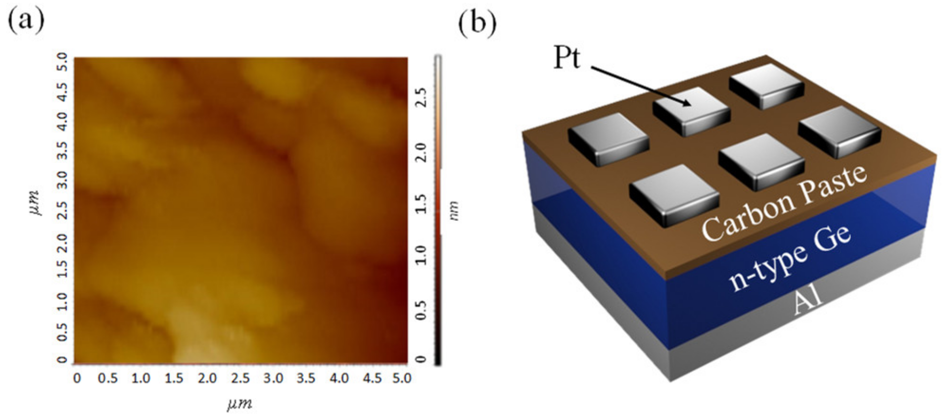
2.1. Materials

This study uses commercial CP from Alfa Aesar Co., Ltd. (Haverhill, MA, USA) (42465, alcohol-based) and n-type Ge (100) substrates, having a carrier concentration of 5.0 × 1015 cm−3. The CP films were then spin-coated at 5000 rpm for 60 s, followed by pre-baking at 60 °C in an ambient atmosphere for 15 min on a hotplate. The sample was then sintered in a furnace in an Ar atmosphere at 300 °C for 30 min.

2.2. Characterization

The thickness of the CP film was ~70 nm, as measured using a profilometer. Atomic force microscopy (AFM) was used to determine the surface morphology of the CP films. The surface morphology of a CP film is quite smooth, as shown in Figure 1a. The root-mean-square (rms) roughness value for a CP film is 0.915 nm. Pt eletrodes (300 × 300 μm2) were produced by means of sputtering through a shadow mask. The structure is shown in Figure 1a. For comparison, a reference device without a CP interlayer was fabricated using the same process conditions. The current–voltage (I–V) curves for the Schottky diodes were measured using a Keithley 2400 sourcemeter. The capacitance–voltage (C–V) plots for the Schottky diodes were recorded using an Agilent E4980A impedance analyzer.

3. Results and Discussion

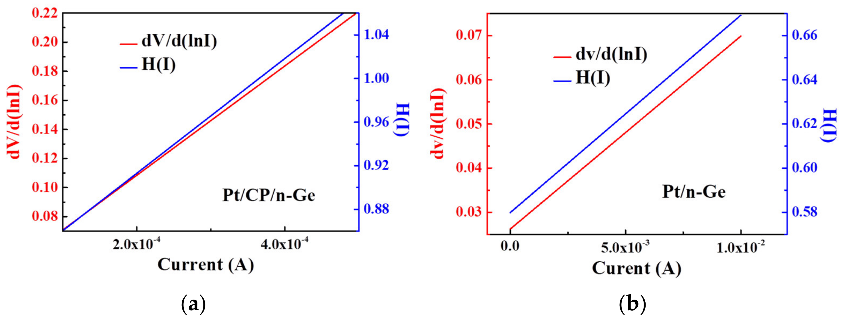
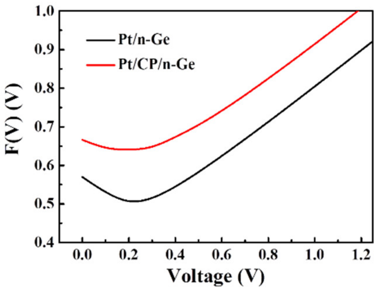
3.1. I–V Characteristics

The effect of an interfacial layer on the electrical characteristics is considered. Figure 2 shows the experimental semi-logarithmic I–V characteristics for Pt/n-type Ge Schottky rectifiers with and without a CP interlayer in the dark. Both diodes exhibit excellent rectification behavior. The characteristic properties of the rectifying contact behavior mean that a reverse bias current has no significant effect on the voltage and there is an exponential increase in the forward bias current. A higher current rectification ratio is achieved for a Pt/CP/n-Ge Schottky junction (234) than for its counterpart (20). Figure 2 shows that the leakage current in reverse bias for Pt/CP/n-Ge Schottky junction is less than that for the counterpart, which demonstrates that the CP interlayer creates an effective barrier between Pt and Ge.
Besides, owing to the existence of bulk resistance of the CP interlayer, there is an obvious decrease at high current for the Pt/CP/n-Ge Schottky junction in the forward bias I–V plot. Standard thermionic emission theory is used to examine the electrical properties for a Schottky diode, which is given as follows [19]:
I = A A * T 2 exp ( q Φ B k T ) exp q ( V I R S ) n k T 1
where A* is the Richardson constant for Ge, which is 140 A cm−2K−2; ΦB,IV is the barrier height; k is the Boltzmann constant; q is the electronic charge; Rs is the series resistance; and n is an ideality factor [12]. The extracted parameters for Schottky diodes are listed in Table 1. For Pt/n-Ge and Pt/CP/n-Ge Schottky junctions, ΦB, IV and n are 0.57 eV and 1.08 and 0.65 eV and 1.95, respectively. The value of ΦB, IV for the studied diode (0.65 eV) is higher than that for the counterpart (0.57 eV). The CP layer produces a higher barrier of 0.08 eV. This result is in agreement with the results of previous reports [11,13]. An organic interlayer prevents direct contact between the metal and Ge surface and significantly changes the interface states, even though the organic/inorganic interface is abrupt and unreactive [20,21,22]. A conventional Ge Schottky contact generally has a strong Fermi-level pinning effect, which leads to poor device performance (i.e., high n and low ΦB). This result is attributed to the metal-induced gap states. Ion bombardment during plasma processing is another possible reason that the surface of the Ge substrate is destroyed, which induces defects and intermixing in the films. The values for n and ΦB for the reference diode for this study (n = 1.08; ΦB = 0.57) are comparable to those reported by previous studies [11,12,13]. Further improvement in the future is possible. For a conventional Schottky diode, the value for n is close to unity. This result shows that the diode current is mainly due to diffusion current and the pure thermionic emission theory fits well. However, the value for n for a Pt/CP/n-Ge Schottky junction is much higher than unity, possibly because of secondary mechanisms, such as CP of uneven thickness, series resistance, and a non-uniform distribution of dipoles due to the presence of an organic interfacial layer [23,24,25,26]. This phenomenon is also noted in previous studies that use an organic interfacial layer for Schottky diodes [11,12,13]. The exact reason for a higher n value is unclear. Generally, an interfacial layer is used to modulate the Schottky barrier height using Fermi level depinning. The value for ΦB increases as the n value increases. The parameters for Pt/CP/n-Ge Schottky diodes could be further optimized.
The plots of Cheung’s function dV/d(InI) versus I and H(I) versus I are used to accurately determine the Schottky parameters, ΦB, H(I), n, and Rs, as shown in Figure 3. Cheung’s function is expressed as follows [12,27]:
d V d ( ln I ) = n k T q + I R S
H ( I ) = V ( n k T q ) ln I A A * T 2
H ( I ) = n Φ B , H ( I ) + I R S
The plot of dV/d(In I) versus I is linear with a gradient of Rs and the y-intercept gives the ideality factor n. The respective values of Rs and n are 4.37 Ω and 1.01 for the Pt/n-Ge Schottky diode, and 376 Ω and 1.28 for the Pt/CP/n-Ge Schottky diode. The H(I) versus I plot is a straight line and the y-axis intercept gives the value for ΦB, H(I). The gradient of this plot can also be used to determine the value of Rs. From the H(I) versus I plot, the Rs and ΦB, H(I) values are 8.93 Ω and 0.57 eV for the Pt/n-Ge Schottky junction and 459 Ω and 0.65 eV for the Pt/CP/n-Ge Schottky junction. The large difference in the values is attributed to a deviation from the ideal model due to the insertion of the CP layer, so the value of Rs is higher [28]. The higher Rs limits the forward current, as shown in Figure 2. An additional decrease in voltage across the CP interlayer produces forward current conduction at a high voltage.
The values of ΦB, Norde and Rs for Schottky junctions are also derived using the modified Norde function, which is expressed as follows [29]:
F ( V ) = V γ k T q ln ( I ( V ) A A * T 2 )
where I(V) is the current obtained from the I-V curves and γ is an integer (dimensionless) that is greater than the value of n. Figure 4 presents the Norde plot as function of applied bias for Pt/n-Ge and Pt/CP/n-Ge Schottky junctions. The minimum point is used to obtain the corresponding voltage that is applied across the device. The value of ΦB, Norde is derived using the following equation [29,30]:
Φ B , N o r d e = F ( V 0 ) + V 0 γ k T q
where F(V0) is the minimum point of F(V) and V0 is the corresponding voltage. The value of Rs is determined using the following relation:
R S = k T ( γ n ) q I 0
where I0 is the minimum point of F(V0). The values for Rs and ΦB, Norde are calculated as 12.14 Ω and 0.58 eV for the Pt/n-Ge Schottky junction and 2735 Ω and 0.72 eV for the Pt/CP/n-Ge Schottky junction, respectively. The Rs and ΦB, Norde values that are derived using Norde’s function are higher than those derived using Cheung’s method because different fitting intervals are used for the I-V curve. Cheung’s function focuses on the nonlinear region and the Norde plot considers the whole range of the I–V curve in forward bias [28,30]. Even if there is a difference in the values for different fitting techniques, Schottky contacts show reasonably good agreement in terms of the value of ΦB.

3.2. C–V Characteristics

The C–V characteristics of the Schottky diodes are shown in Figure 5. The capacitance of the depletion layer is described using a standard Mott–Schottky relationship [31]:
1 C 2 = 2 ( V b i V ) A 2 q ε S ε 0 N
where A is the surface area, εs is the permittivity, ε0 is the dielectric constant, Vbi is the built-in potential, and N is the carrier concentration. The x-intercept is Vbi. The gradient is N. The value of ΦB, CV can be calculated as follows [31]:
Φ B , C V = Φ b i + k T q ln N C N
where Nc is the conduction band density states of 1.0 × 10⁻¹⁹ cm−3 [12]. A list of electronic parameters for the Schottky diodes is given in Table 1. The C–V characteristics give a barrier height of 0.90 eV for a Ge Schottky diode with a CP interlayer and 0.82 eV for a Pt/n-type Ge Schottky diode with no CP interlayer. The increase of ΦB, CV is consistent with the results of I–V measurements when there is a CP interlayer. There is a relatively large discrepancy between the value for ΦB, IV and ΦB, CV because the conduction mechanism in these diodes does not exactly obey the thermionic emission theory. The values of ΦB, IV derived from the I–V curve are sensitive to image force due to the current flow across the barrier [32]. The values of ΦB, CV derived from the C–V curve are insensitive to potential fluctuations because the scale is much shorter than the space charge region [33]. The C–V measurement gives an average barrier height for the entire diode, but the current flows preferentially through the barrier minima during I–V measurement [33]. The difference between C–V and I–V measurement techniques results in different results for Schottky barrier height [34].

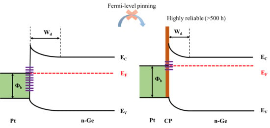
3.3. Energy Band Diagrams

The role of the CP interlayer for Pt/CP/n-Ge Schottky diodes is demonstrated using an energy diagram, as shown in Figure 6. At the metal/semiconductor interface, there are many dangling bonds, so there is a strong Fermi level pinning effect, as shown in Figure 6a. CP is an interlayer that conducts charged carriers with tiny resistance. The CP interlayer play a role of a dangling bond terminator at the Ge surface (Figure 6b).

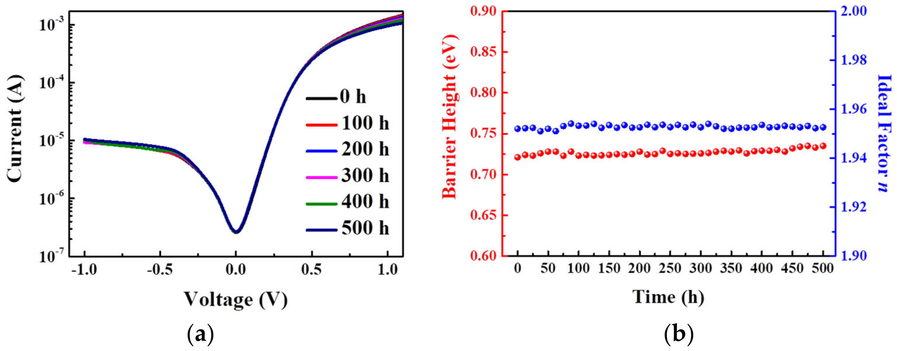
3.4. Long-Term Reliability

Long-term reliability is a key factor for a diode for real applications [35,36,37]. To the best of the author’s knowledge, there is no standard specification involving stability tests for Schottky diodes. To determine the long-term reliability of the CP interlayer, a Schottky diode with CP was driven under 0.1 A under ambient conditions, with no encapsulation or humidity control, over a period of 500 h. The fluctuation in ΦB and n is negligible over the time of the test, as shown in Figure 7a,b. The organic layer is the only source for device degradation because the crystalline Ge and metals are relatively stable in air. Compared with the emerging organic layer for a Pt/n-Ge Schottky diode, such as PEDOT/PSS, the ambient stability for the device is poor because a PEDOT/PSS film contains water soluble ionic PSS [13]. The sheet resistance for pristine PEDOT/PSS film increases by more than 20% after storage in air for 1 week [38]. In addition, the carbon-containing diode exhibits long-term stability under a DC bias, which is attributed to the excellent thermal stability of CP. When current flows cross a contact, spot heat is generated in the constriction resistance [39], which decreases the performance of an organic semiconductor. CP is primarily composed of graphite powder and graphite is resistant to high temperatures [18]. Therefore, commercially available CP is eminently suited to the fabrication of highly stable and efficient Schottky diodes.

4. Conclusions

An organic–inorganic structure is formed using a CP thin film as an interlayer for a Pt/n-Ge Schottky diode. To determine the electrical characteristics of the Pt/CP/n-Ge Schottky diodes, the I–V and C–V characteristics are measured at room temperature. This structure exhibits better rectifying behavior and results in a higher barrier height than a conventional Pt/n-Ge diode because the effective barrier height is increased when there is a CP interlayer. This study shows that CP is a reliable interlayer for an inorganic–organic hybrid Schottky diode.

Author Contributions

Conceptualization, P.-T.L.; methodology, J.-W.C., S.-R.C. and Z.-K.L.; formal analysis, W.-Z.C., J.-H.H. and Y.-Z.J.; writing—original draft preparation, P.-T.L.; writing—review and editing, P.-T.L.; supervision, W.-J.H. and C.-Y.H. All authors have read and agreed to the published version of the manuscript.

Funding

This research was funded by Ministry of Science and Technology of Taiwan under Contract No. MOST 106-2218-E-260-001-MY3.

Data Availability Statement

The data presented in this study are contained in this article.

Acknowledgments

This work is supported by the Ministry of Science and Technology of Taiwan under grant No. MOST 106-2218-E-260-001-MY3.

Conflicts of Interest

The authors declare no conflict of interest.

References

  1. Chawanda, A.; Coelho, S.M.M.; Auret, F.D.; Mtangi, W.; Nyamhere, C.; Nel, J.M.; Diale, M. Effect of thermal treatment on the characteristics of iridium Schottky barrier diodes on n-Ge (100). J. Alloy. Compd. 2012, 513, 44–49. [Google Scholar] [CrossRef] [Green Version]
  2. Ruan, D.-B.; Chang-Liao, K.-S.; Hong, Z.-Q.; Huang, J.; Yi, S.-H.; Liu, G.-T.; Chiu, P.-C.; Li, Y.-L. Radiation effects and reliability characteristics of Ge pMOSFETs. Microelectron. Eng. 2019, 216. [Google Scholar] [CrossRef]
  3. Pfeiffer, U.R.; Mishra, C.; Rassel, R.M.; Pinkett, S.; Reynolds, S.K. Schottky Barrier Diode Circuits in Silicon for Future Millimeter-Wave and Terahertz Applications. IEEE Trans. Microw. Theory Tech. 2008, 56, 364–371. [Google Scholar] [CrossRef]
  4. Lou, X.; Zhang, W.; Xie, Z.; Yang, L.; Yu, X.; Liu, Y.; Chang, H. Solution-processed high-k dielectrics for improving the performance of flexible intrinsic Ge nanowire transistors: Dielectrics screening, interface engineering and electrical properties. J. Phys. D Appl. Phys. 2019, 52. [Google Scholar] [CrossRef]
  5. Khurelbaatar, Z.; Kil, Y.-H.; Shim, K.-H.; Cho, H.; Kim, M.-J.; Kim, Y.-T.; Choi, C.-J. Temperature Dependent Current Transport Mechanism in Graphene/Germanium Schottky Barrier Diode. JSTS J. Semicond. Technol. Sci. 2015, 15, 7–15. [Google Scholar] [CrossRef] [Green Version]
  6. Chawanda, A.; Nyamhere, C.; Auret, F.D.; Mtangi, W.; Diale, M.; Nel, J.M. Thermal annealing behaviour of platinum, nickel and titanium Schottky barrier diodes on n-Ge (100). J. Alloy. Compd. 2010, 492, 649–655. [Google Scholar] [CrossRef]
  7. Chen, Z.; Yuan, S.; Li, J.; Zhang, R. Thermal Stability Enhancement of NiGe Metal Source/Drain and Ge pMOSFETs by Dopant Segregation. IEEE Trans. Electron Devices 2019, 66, 5284–5288. [Google Scholar] [CrossRef]
  8. Lee, H.-K.; Jyothi, I.; Janardhanam, V.; Shim, K.-H.; Yun, H.-J.; Lee, S.-N.; Hong, H.; Jeong, J.-C.; Choi, C.-J. Effects of Ta-oxide interlayer on the Schottky barrier parameters of Ni/n-type Ge Schottky barrier diode. Microelectron. Eng. 2016, 163, 26–31. [Google Scholar] [CrossRef]
  9. Zhou, Y.; Ogawa, M.; Han, X.; Wang, K.L. Alleviation of Fermi-level pinning effect on metal/germanium interface by insertion of an ultrathin aluminum oxide. Appl. Phys. Lett. 2008, 93. [Google Scholar] [CrossRef]
  10. Zhou, Y.; Han, W.; Wang, Y.; Xiu, F.; Zou, J.; Kawakami, R.K.; Wang, K.L. Investigating the origin of Fermi level pinning in Ge Schottky junctions using epitaxially grown ultrathin MgO films. Appl. Phys. Lett. 2010, 96. [Google Scholar] [CrossRef] [Green Version]
  11. Kumar, A.A.; Reddy, V.R.; Janardhanam, V.; Seo, M.-W.; Hong, H.; Shin, K.-S.; Choi, C.-J. Electrical Properties of Pt/n-Ge Schottky Contact Modified Using Copper Phthalocyanine (CuPc) Interlayer. J. Electrochem. Soc. 2011, 159, H33–H37. [Google Scholar] [CrossRef]
  12. Jyothi, I.; Janardhanam, V.; Rajagopal Reddy, V.; Choi, C.-J. Modified electrical characteristics of Pt/n-type Ge Schottky diode with a pyronine-B interlayer. Superlattices Microstruct. 2014, 75, 806–817. [Google Scholar] [CrossRef]
  13. Ashok Kumar, A.; Rajagopal Reddy, V.; Janardhanam, V.; Yang, H.-D.; Yun, H.-J.; Choi, C.-J. Electrical properties of Pt/n-type Ge Schottky contact with PEDOT:PSS interlayer. J. Alloy. Compd. 2013, 549, 18–21. [Google Scholar] [CrossRef]
  14. Enver Aydin, M.; Yakuphanoglu, F. Electrical characterization of inorganic-on-organic diode based InP and poly(3,4-ethylenedioxithiophene)/poly(styrenesulfonate) (PEDOT:PSS). Microelectron. Reliab. 2012, 52, 1350–1354. [Google Scholar] [CrossRef]
  15. Huang, C.-Y.; Lin, P.-T.; Cheng, H.-C.; Lo, F.-C.; Lee, P.-S.; Huang, Y.-W.; Huang, Q.-Y.; Kuo, Y.-C.; Lin, S.-W.; Liu, Y.-R. Rectified Schottky diodes that use low-cost carbon paste/InGaZnO junctions. Org. Electron. 2019, 68, 212–217. [Google Scholar] [CrossRef]
  16. Huang, C.-Y.; Lin, G.-Y.; Lin, P.-T.; Chen, J.-W.; Chen, C.-H.; Chien, F.S.-S. Influences of sintering temperature on low-cost carbon paste based counter electrodes for dye-sensitized solar cells. Jpn. J. Appl. Phys. 2017, 56. [Google Scholar] [CrossRef]
  17. Gao, Y.; Chu, L.; Wu, M.; Wang, L.; Guo, W.; Ma, T. Improvement of adhesion of Pt-free counter electrodes for low-cost dye-sensitized solar cells. J. Photochem. Photobiol. A Chem. 2012, 245, 66–71. [Google Scholar] [CrossRef]
  18. Mishraa, A.; Ahmadb, Z.; Zimmermannc, I.; Martineaud, D.; Shakoorb, R.A.; Touatia, F.; Riaze, K.; Al-Muhtasebf, S.A.; Nazeeruddinc, M.K. Effect of annealing temperature on the performance of printable carbon electrodes for perovskite solar cells. Org. Electron. 2019, 65, 375–380. [Google Scholar] [CrossRef]
  19. Chasin, A.; Steudel, S.; Myny, K.; Nag, M.; Ke, T.-H.; Schols, S.; Genoe, J.; Gielen, G.; Heremans, P. High-performance a-In-Ga-Zn-O Schottky diode with oxygen-treated metal contacts. Appl. Phys. Lett. 2012, 101. [Google Scholar] [CrossRef]
  20. Sreenu, K.; Venkata Prasad, C.; Rajagopal Reddy, V. Barrier Parameters and Current Transport Characteristics of Ti/p-InP Schottky Junction Modified Using Orange G (OG) Organic Interlayer. J. Electron. Mater. 2017, 46, 5746–5754. [Google Scholar] [CrossRef]
  21. Tan, S.O.; Tecimer, H.; Cicek, O. Comparative Investigation on the Effects of Organic and Inorganic Interlayers in Au/n-GaAs Schottky Diodes. IEEE Trans. Electron Devices 2017, 64, 984–990. [Google Scholar] [CrossRef]
  22. Tan, S.O. Comparison of Graphene and Zinc Dopant Materials for Organic Polymer Interfacial Layer Between Metal Semiconductor Structure. IEEE Trans. Electron Devices 2017, 64, 5121–5127. [Google Scholar] [CrossRef]
  23. Winfried, M. Barrier heights of real Schottky contacts explained by metal-induced gap states and lateral inhomogeneities. J. Vac. Sci. Technol. B 1999, 17. [Google Scholar] [CrossRef]
  24. Lonergan, M.C.; Jones, F.E. Calculation of transmission coefficients at nonideal semiconductor interfaces characterized by a spatial distribution of barrier heights. J. Chem. Phys. 2001, 115, 433. [Google Scholar] [CrossRef]
  25. Gullu, O.; Cankaya, M.; Baris, O.; Biber, M.; Ozdemir, H.; Gulluce, M.; Turut, A. DNA-based organic-on-inorganic semiconductor Schottky structures. Appl. Surf. Sci. 2008, 254, 5175–5180. [Google Scholar] [CrossRef]
  26. Gullu, O.; Aydogan, S.; Turut, A. High barrier Schottky diode with organic interlayer. Solid State Commun. 2012, 152, 381–385. [Google Scholar] [CrossRef]
  27. Cheung, S.K.; Cheung, N.W. Extraction of Schottky diode parameters from forward current-voltage characteristics. Appl. Phys. Lett. 1986, 49, 85–87. [Google Scholar] [CrossRef]
  28. Aubry, V.; Meyer, F. Schottky diodes with high series resistance: Limitations of forwardI-Vmethods. J. Appl. Phys. 1994, 76, 7973–7984. [Google Scholar] [CrossRef]
  29. Norde, H. A modified forward I-V plot for Schottky diodes with high series resistance. J. Appl. Phys. 1979, 50, 5052–5053. [Google Scholar] [CrossRef]
  30. Ocak, Y.S.; Guven, R.G.; Tombak, A.; Kilicoglu, T.; Guven, K.; Dogru, M. Barrier height enhancement of metal/semiconductor contact by an enzyme biofilm interlayer. Philos. Mag. 2013, 93, 2172–2181. [Google Scholar] [CrossRef]
  31. Du, L.; Li, H.; Yan, L.; Zhang, J.; Xin, Q.; Wang, Q.; Song, A. Effects of substrate and anode metal annealing on InGaZnO Schottky diodes. Appl. Phys. Lett. 2017, 110. [Google Scholar] [CrossRef] [Green Version]
  32. Xin, Q.; Yan, L.; Luo, Y.; Song, A. Study of breakdown voltage of indium-gallium-zinc-oxide-based Schottky diode. Appl. Phys. Lett. 2015, 106. [Google Scholar] [CrossRef]
  33. Zhang, J.; Wang, H.; Wilson, J.; Ma, X.; Jin, J.; Song, A. Room Temperature Processed Ultrahigh-Frequency Indium-Gallium–Zinc-Oxide Schottky Diode. IEEE Electron Device Lett. 2016, 37, 389–392. [Google Scholar] [CrossRef]
  34. Xin, Q.; Yan, L.; Du, L.; Zhang, J.; Luo, Y.; Wang, Q.; Song, A. Influence of sputtering conditions on room-temperature fabricated InGaZnO-based Schottky diodes. Thin Solid Film. 2016, 616, 569–572. [Google Scholar] [CrossRef]
  35. Zou, C.; Huang, C.Y.; Sanehira, E.M.; Luther, J.M.; Lin, L.Y. Highly stable cesium lead iodide perovskite quantum dot light-emitting diodes. Nanotechnology 2017, 28, 455201. [Google Scholar] [CrossRef] [PubMed]
  36. Huang, C.-Y.; Zou, C.; Mao, C.; Corp, K.L.; Yao, Y.-C.; Lee, Y.-J.; Schlenker, C.W.; Jen, A.K.Y.; Lin, L.Y. CsPbBr3 Perovskite Quantum Dot Vertical Cavity Lasers with Low Threshold and High Stability. ACS Photonics 2017, 4, 2281–2289. [Google Scholar] [CrossRef]
  37. Qian, H.; Wu, C.; Lu, H.; Xu, W.; Zhou, D.; Ren, F.; Chen, D.; Zhang, R.; Zheng, Y. Bias stress instability involving subgap state transitions in a-IGZO Schottky barrier diodes. J. Phys. D Appl. Phys. 2016, 49. [Google Scholar] [CrossRef]
  38. Kim, S.; Sanyoto, B.; Park, W.-T.; Kim, S.; Mandal, S.; Lim, J.-C.; Noh, Y.-Y.; Kim, J.-H. Purification of PEDOT:PSS by Ultrafiltration for Highly Conductive Transparent Electrode of All-Printed Organic Devices. Adv. Mater. 2016, 46. [Google Scholar] [CrossRef]
  39. Williamson, J.B.P.; Allen, N. Thermal stability in graphite contacts. Wear 1982, 78, 38–49. [Google Scholar] [CrossRef]
Figure 1. (a) Atomic force microscopy (AFM) image of a carbon paste (CP) film and (b) device structure of a Pt/CP/n-Ge Schottky diode.
Crystals 11 00259 g001
Figure 2. Experimental I–V curves for Pt/n-Ge Schottky diodes with and without a CP interlayer.
Crystals 11 00259 g002
Figure 3. Plots of dV/d(InI) versus I and H(I) versus I using diode Equation (1) for Pt/n-Ge Schottky diodes (a) with and (b) without a CP interlayer.
Crystals 11 00259 g003
Figure 4. Norde plot for Pt/n-Ge Schottky diodes with and without a CP interlayer, using the diode Equation (1).
Crystals 11 00259 g004
Figure 5. A2/C2–V characteristics for Pt/n-Ge Schottky diodes with and without a CP interlayer.
Crystals 11 00259 g005
Figure 6. Energy band diagrams for Pt/n-Ge Schottky diodes (a) with and (b) without a CP interlayer.
Crystals 11 00259 g006
Figure 7. (a) I–V characteristics for a Pt/CP/n-Ge Schottky diode for different DC stress (0.1 A) times and (b) ΦB and n as a function of stress time, as obtained from the diode equation (1): the measurements were performed at room temperature in ambient conditions.
Crystals 11 00259 g007
Table 1. Schottky diode parameters derived using various methods. CP, carbon paste.
I–VdV/d(lnI) vs. IH(I) vs. INordeC–V
ΦB (eV) nRS(Ω)nRS(Ω)ΦB (eV) RS(Ω)ΦB (eV) ΦB (eV)
w/o CP0.571.084.371.018.930.5712.140.580.82
w/i CP0.651.953761.284590.6527350.720.9
Publisher’s Note: MDPI stays neutral with regard to jurisdictional claims in published maps and institutional affiliations.

