Article

Polyethylenimine-Ethoxylated Interfacial Layer for Efficient Electron Collection in SnO2-Based Inverted Organic Solar Cells

1
Optics & Photonics Center, MAScIR, Rabat BP 10100, Morocco
2
Faculty of Sciences, Mohammed V University, Rabat BP 1014, Morocco
3
Institut de Physique et Chimie des Matériaux de Strasbourg, CNRS UMR 7504, Université de Strasbourg, BP 43, F-67034 Strasbourg CEDEX 2, France
4
Laboratoire des Sciences de l’Ingénieur, de l’Informatique et de l’Imagerie, CNRS UMR 7357, Université de Strasbourg, BP 20, F-67037 Strasbourg CEDEX 2, France
*
Authors to whom correspondence should be addressed.
Crystals 2020, 10(9), 731; https://doi.org/10.3390/cryst10090731
Submission received: 20 June 2020 / Revised: 11 July 2020 / Accepted: 14 July 2020 / Published: 20 August 2020
(This article belongs to the Special Issue Organic Photovoltaic)

Abstract

:
In this work, we studied inverted organic solar cells based on bulk heterojunction using poly(3-hexylthiophene-2,5-diyl):[6,6]-phenyl-C71-butyric acid methyl ester (P3HT:PCBM) as an active layer and a novel cathode buffer bilayer consisting of tin dioxide (SnO2) combined with polyethylenimine-ethoxylated (PEIE) to overcome the limitations of the single cathode buffer layer. The combination of SnO2 with PEIE is a promising approach that improves the charge carrier collection and reduces the recombination. The efficient device, which is prepared with a cathode buffer bilayer of 20 nm SnO2 combined with 10 nm PEIE, achieved Jsc = 7.86 mA/cm2, Voc = 574 mV and PCE = 2.84%. The obtained results exceed the performances of reference solar cell using only a single cathode layer of either SnO2 or PEIE.

Graphical Abstract

1. Introduction

Third-generation photovoltaic technology based on conjugated polymers has drawn much attention over the past decade due to advantages such as simple preparation, light weight, low cost, solution-based fabrication on large-area and low-temperature solution process ability that allows for fabrication on flexible substrates via roll-to-roll manufacturing for solar energy conversion [1,2,3,4]. Recently, efforts have been made to enhance power conversion efficiency (PCE) of organic solar cells (OSCs), reaching a power conversion efficiency above 15–17% [5,6]. To do so, the research was focused on the development of device architecture [7,8,9], design semiconductor polymers and development of non-fullerene acceptors (e.g.,2,2′-[[6,6,12,12-Tetrakis(4-hexylphenyl)-6,12- dihydrodithieno[2,3-d:2′,3′-d′]-s-indaceno[1,2-b:5,6-b′]dithiophene-2,8-diyl]bis[methylidyne (3-oxo-1H-indene-2,1(3H)-diylidene)]]bis[propanedinitrile] family (ITIC))[10,11,12], controlmorphology [13,14] and interfacial engineering between layer materials and the active layer that provides a powerful strategy to enhance both stability and efficiency of organic photovoltaic devices. Generally, the structure of OSCs could be classified into two categories, namely conventional and inverted structures; the conventional architecture is based on a bulk heterojunction active layer sandwiched between a transparent conducting electrode, such as indium tin oxide (ITO), and a low work function metal electrode (Ca/Al, LiF/Al or Al) [15]. On one hand, one of the major problems for the conventional structure is the long-term stability when exposed to air due to the use of a cathode that is sensitive to air and moisture, which leads to its rapid oxidation. On the other hand, poly(3,4 ethylenedioxythiophene):polystyrene sulfonic acid (PEDOT:PSS) has an acidic and hydrophilic nature [16,17], which is detrimental to the active layer and can etch the ITO via the increase of the interfacial resistance through indium diffusion into the active layer; this leads to the deterioration of the device performance [18,19,20]. To overcome these issues, the inverted configuration is the appropriate solution to make PEDOT:PSS-free device, where the polarity of charge collection is opposite to that in the conventional one. Inverted organic solar cell (iOSC) configuration allows the use of high work function metal contact that is less air-sensitive, and a low work function metal oxide as electron transporting layer to modify the ITO surface.
Current researchers have used several methods to improve iOSC performance, including using a metal oxide layer as an electron transporting layer (ETL) between the active layer and the ITO cathode, which is indispensable so that ohmic contact for the decrease or elimination of the electron-extraction barrier can be formed. N-type metal oxides such as titanium oxide (TiOx), zinc oxide (ZnO) and tin oxide (SnO2) can be introduced as a cathode buffer layer (CBL) to modify ITO as an effective electron-collecting electrode in inverted OSCs [21,22,23].
In particular, tin dioxide (SnO2) has recently received more attention as an interfacial material for organic photovoltaic (OPV) devices because of its beneficial properties, namely good optical transparency, high resistivity, high electron mobility, high transmittance in visible region and high chemical and thermal stabilities compared to other transparent conductive oxides [24,25]. Several works have studied the effect of SnO2 on the inverted organic solar cell performance [26,27]. An efficiency of 4.05% was achieved by a Korean group using P3HT:PCBM absorber materials and aqueous solution processed SnO2 combined with ionic liquid (IL) as a buffer layer. Besides this work, Shuai Huang et al. [28] deposited SnO2 by a sol–gel process in a P3HT:PC71BM-based inverted solar cell, and they obtained an efficiency of 4.25%.
Nowadays, polyethylenimine-ethoxylated (PEIE) is used as an interlayer to reduce the electrode material’s work function (WF). PEIE contains simple aliphatic amine groups that can produce surface dipoles; as a consequence, the WF of the ITO electrode decreases [29,30,31]. The created interfacial dipole induces a vacuum level shift, which effectively causes a reduction of the WF of the underlying electrode [32,33,34,35]. Recently, Courtright et al. [36] studied separately PEIE and PEI as the ETL for PBDTT-FTTE:PC70BM-based iOPVs on top of zinc oxide. They found that the incorporation of PEIE as a cathode buffer layer gave an enhancement of the cell performance with 7.37%. Using PEI, an efficiency of 8.22% was reached.
In the present study, the work is devoted to an inverted organic solar cell based on bulk heterojunction using poly (3-hexylthiophene-2,5-diyl):[6,6]-phenyl-C71-butryric acid methyl ester (P3HT:PCBM) as an absorber. The originality of our study is to overcome the limitations of the use of a single cathode buffer layer, using the cathode buffer bilayer tin dioxide (SnO2) with PEIE. The SnO2 layer was deposited by magnetron reactive sputtering with different thicknesses, and then PEIE thin film was deposited via an aqueous solution-process. It has been found that with the combination of SnO2 and PEIE as a cathode buffer bilayer, the short circuit current density (Jsc) was obviously improved, resulting in better device performance with an efficiency reaching 2.84%, compared to reference devices with pure SnO2 and PEIE as a cathode buffer layer.

2. Characterization Set-Up

Structural, morphological and optical properties of the prepared films as well as the inverted devices were analyzed with different techniques. The films were analyzed by X-ray diffraction (XRD) and grazing incident X-ray diffraction (GIXRD) in the 20°–80° 2θ range by means of a Rigaku Smartlab® diffractometer (9 kW) equipped with a CuKα1 incident source (λ = 1.54056 Å) and a Ge (220) × 2-bounce front monochromator. Morphological analysis was carried out by scanning electron microscopy (SEM) on a Zeiss GEMINI 500 scanning electron microscope. A UV–Visible–NIR spectrophotometer (Perkin-Elmer Lambda 950) with an integrating sphere of 150 mm was used to obtain the transmission/absorption spectra of the films in the wavelength range of 200–1000 nm. Atomic force microscopy (AFM) images were obtained in tapping mode with a Nanoscope Dimension 3100 from Veeco Instruments. Scanning electron microscopy (SEM) images were recorded by JEOL 6700F microscope. The resistivity, carrier concentration and Hall mobility of the SnO2 films were determined by a Hall effect measurement system at room temperature using ECOPIA equipment (HMS-5500 Van der Pauw). The electrical characterizations of the inverted devices were done inside a glovebox under a nitrogen atmosphere; the current density–voltage (J–V) characteristics were measured with an HP Agilent source measurement unit, in dark and under illumination using a solar simulator with AM1.5G conditions (Oriel Xenon 150 W, model 96000), after calibration using a standard silicon solar cell with 100 mW/cm2. The external quantum efficiency (EQE) was also measured inside the glovebox for the elaborated devices.

3. Experimental Section

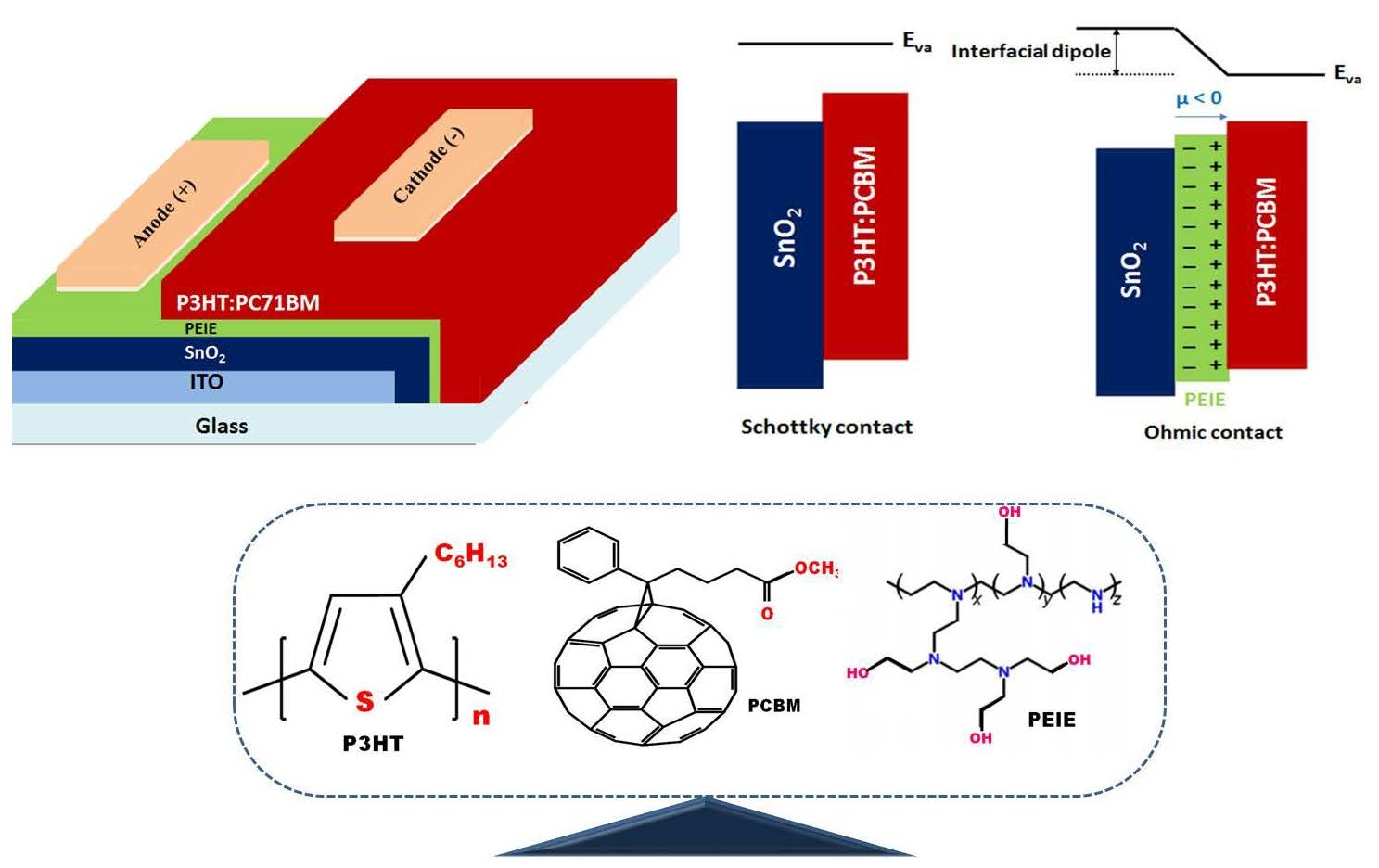
3.1. Thin Film Preparation

3.1.1. SnO2 Thin Film Deposition

The cleaning process of the pre-patterned ITO (sheet resistance 5–15 Ω, Lumtec) glass substrates was done in an ultrasonic bath successively in detergent, deionized water, acetone, 2-isopropanol and de-ionized water, then dried with nitrogen gas flow followed by UV-ozone treatment for 15 min. SnO2 layers were deposited onto clean ITO at 200 °C by radio frequency (RF) reactive magnetron sputtering in a commercial sputtering system (Orion 3 device from AJA International Co.) using pure target of Sn (99.99%). The SnO2 sputtering was done in an argon–oxygen gas mixture, with 8 sccm argon and 4 sccm oxygen. The sputtering parameters used in this work were optimized in a previous work [37,38], and the deposition time was varied to deposit different thicknesses of the SnO2 layer: 10, 20, 30, 40 and 60 nm.

3.1.2. PEIE Interlayer Fabrication

PEIE (Mw = 70,000 g/mol, Sigma-Aldrich), an 80% ethoxylated-based solution, was prepared by diluting 0.2% by mass in 2-methoxyethanol (99.8%, Sigma-Aldrich), which was deposited onto ITO/SnO2 substrates by a spin-coater at 1500 rpm for 60s. Afterward, a part of the PEIE was wiped away from the borders with ethanol. Then, the prepared structures were placed inside the nitrogen-filled glove box for further treatment and depositions to complete the device structure; the samples were annealed at 100 °C for 15 min before depositing the active layer.

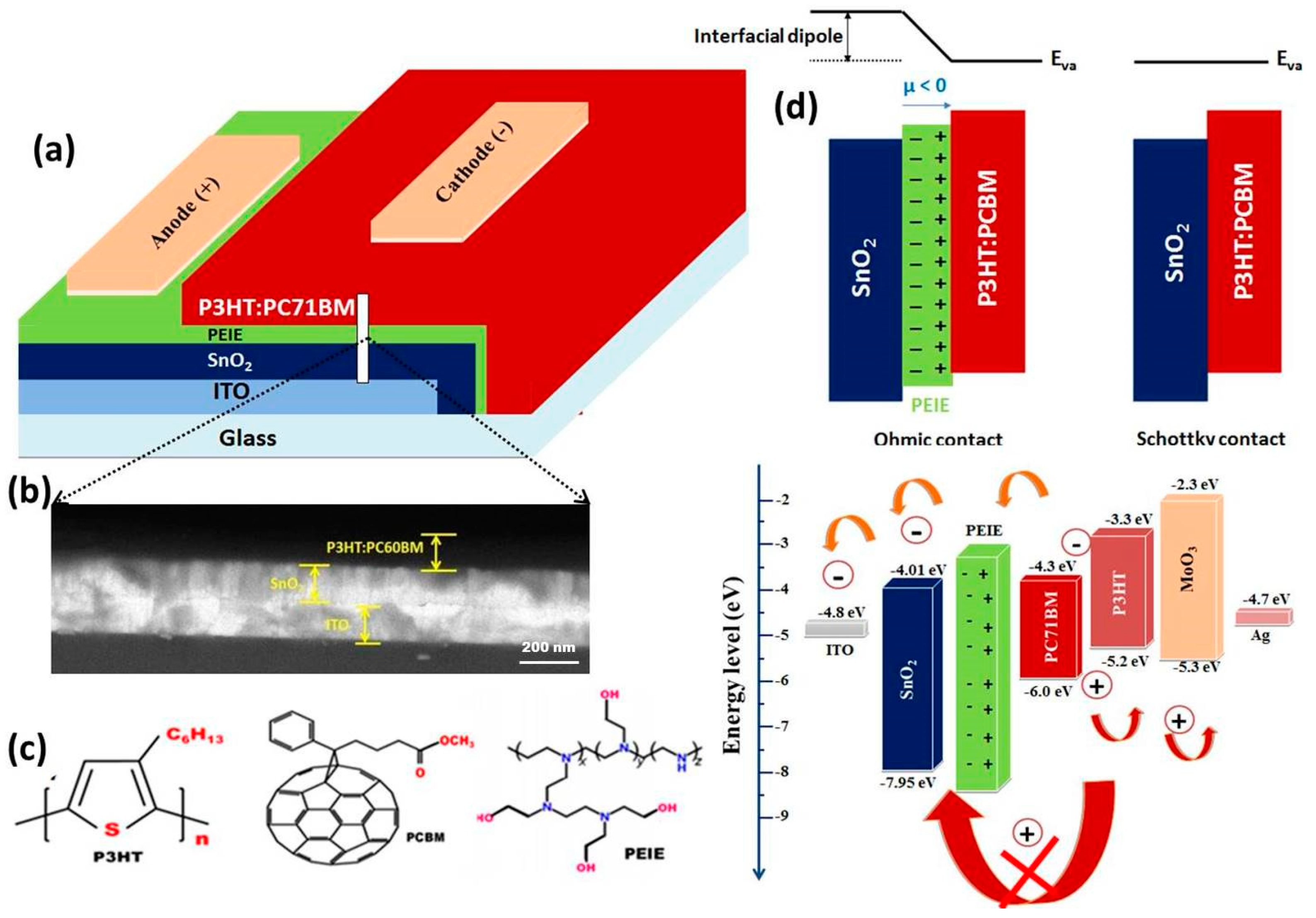
3.1.3. Inverted Device Elaboration

iOSCs were fabricated using P3HT (98.5% regioregular, Sigma-Aldrich) as an electron donor and PC71BM (99.5%, Solenne B.V.) as an electron acceptor. The photo-active layer was prepared based on P3HT:PC71BM solution with a ratio of 1:0.7 dispersed in 1 mL o-dichlorobenzene (99%, anhydrous, Sigma-Aldrich). The absorber layer was deposited onto the previous prepared films using a spin-coater with 1200 rpm for 60s and then annealed at 150 °C for 15 min. Next, MoO3 (7 nm) and Ag (120 nm) were thermally evaporated in a vacuum of 1.10–6 Torr, acting as inverted device electrodes. We fabricated a series of inverted PSC devices with various SnO2 thicknesses of PEIE with the following structure: glass/ITO/SnO2/P3HT:PCBM/MoO3/Ag; another kind of device was also fabricated by incorporating an ultrathin PEIE layer with structure glass/ITO/SnO2/PEIE/P3HT:PCBM/MoO3/Ag. The final architecture of the inverted device (ITO/SnO2/PEIE/P3HT:PCBM/MoO3/Ag) is illustrated in Figure 1a; the device working area was about 0.12 cm2.
The device configuration, chemical structure and energy level diagram of each component are given in Figure 1a,b. Tin dioxide has conduction band and valence band energies around −7.95 eV and −4.01 eV [39], respectively, which suggests that electrons from the active layer can be transported into SnO2, while holes from the active layer can be blocked. At the same time PEIE contains simple aliphatic amine groups that can produce surface dipoles between the cathode and the active layer. Consequently, the work-function of the ETL is significantly reduced beyond the lowest unoccupied molecular orbital (LUMO) value of PCBM. The PEIE layer acts as a stepping stone, which decreases the energy barrier at the interface of the ITO/SnO2 layer and P3HT:PCBM. The electrical contact between the active layer and the ETL shift from a Schottky contact to an ohmic contact. The alignments of the energy levels facilitate electron transport and reduce the energy loss in the process of charge separation, contributing to the enhancement of the short-circuit density (Jsc) and the open-circuit voltage (Voc). Therefore, SnO2 has a relatively wider band gap and lower valence band position, which blocks holes and thus avoids undesirable carrier recombination during the electron transport from the photoactive layers to the ITO cathode.

4. Results and Discussion

4.1. Single Layer

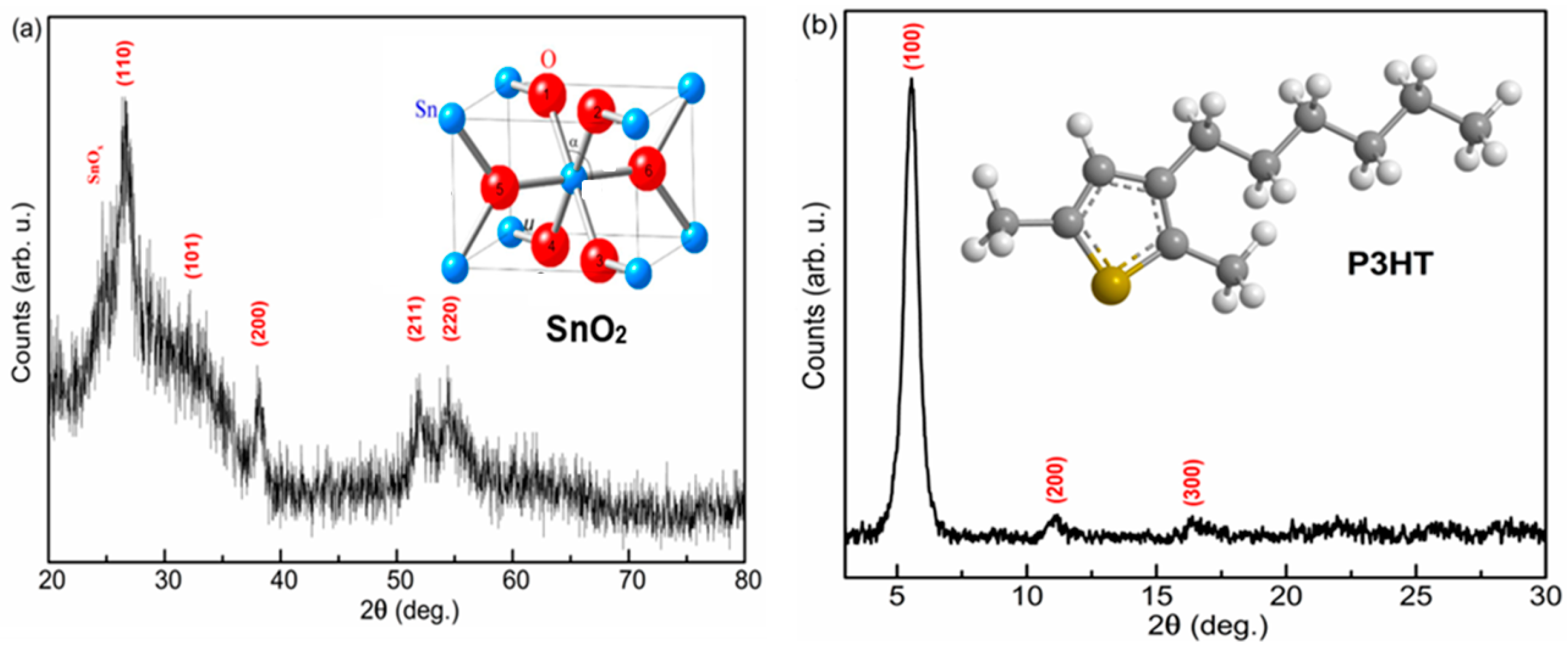
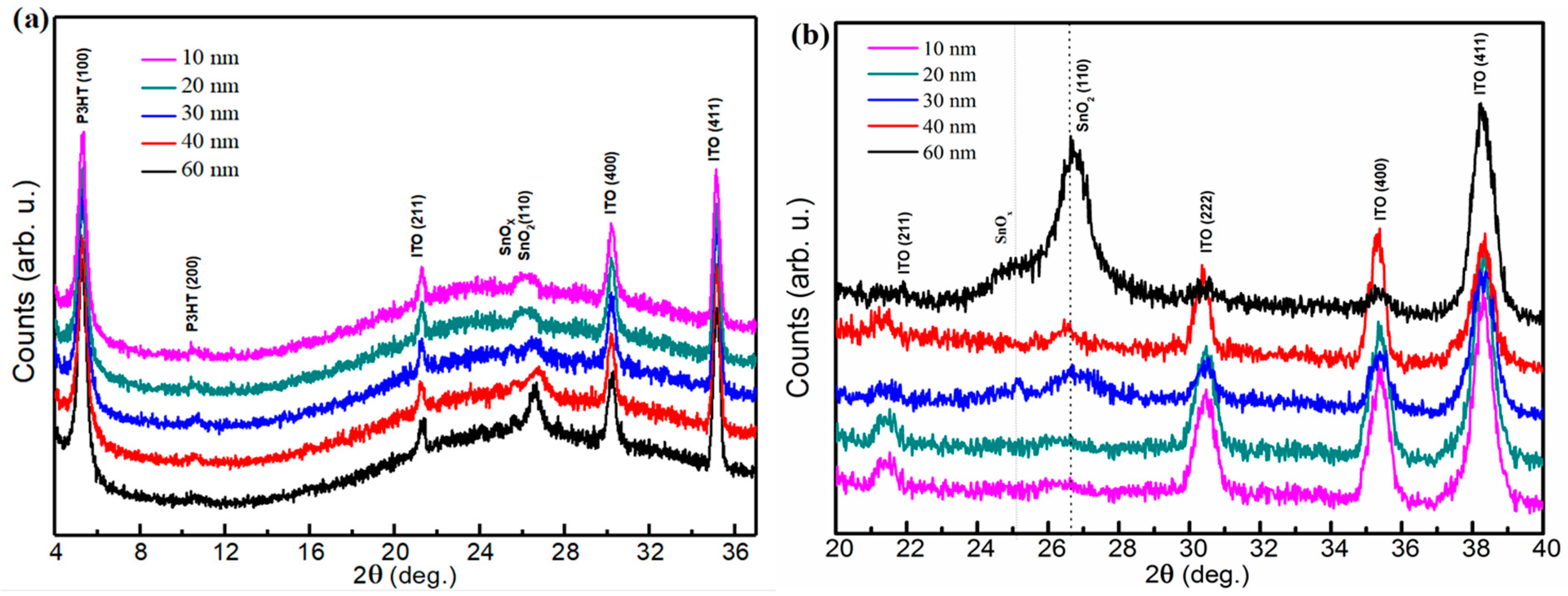
4.1.1. X-ray Diffraction Study

The structural properties of SnO2 and P3HT thin films are depicted in Figure 2. The XRD pattern of SnO2 with 100 nm revealed peaks at 26.66°, 33.89°, 37.94°, 51.77° and 54.75° assigned respectively to planes (110), (101), (200), (211) and (220) of crystalline tin-dioxide tetragonal rutile structure with space group P42/mnm, which matched well with JCPDS card (Joint Committee on Powder Diffraction Standards) no 00-041-1445 and exhibited (101) plane as the preferred orientation. The XRD pattern of P3HT demonstrated a high crystalline structure, with peaks located at low angles 5.3°, 10.7° and 15.90°, which were attributed respectively to planes (100), (200) and (300), with a preferential orientation toward the (100) plane; these peaks were related to lamellar ordering of the phase separated structure by alkyl side chains [40,41].

4.1.2. UV-Visible Study

To investigate the transmittance of SnO2 layers as well as photoactive layer absorption, a UV-visible study was conducted on our samples.
Figure 3a presents the absorption spectra of P3HT, PCBM and the P3HT:PCBM mixture. The conjugated polymer P3HT had a wide and strong absorption band in the range of 400–650 nm and revealed a maximum at ~550 nm. Nevertheless, PCBM presented a broad absorption in ultraviolet in the range of 300–575 nm with a maximum absorption at ~375 nm. One can see that the optical absorption spectra of P3HT:PCBM (1:0.7)-based thin film exhibited a first absorption shoulder at 300–350 nm attributed to PCBM and a second dominant peak located at higher wavelengths corresponding to P3HT absorption. The peak at 450 nm (2.75 eV) corresponded to band-to-band transitions inferred from π–π* transitions from the highest occupied molecular orbital (HOMO) to the lowest unoccupied molecular orbital (LUMO) [42], and this peak was located at a lower photon energy of 2.25 eV for pure pristine P3HT films. The absorption shoulders located at ~600 nm (2.07 eV), ~550 nm (2.25 eV) and ~515 nm (2.41 eV) revealed the three absorption features (S0, S1, S2) of P3HT excitonic absorption with Frenkel excitons absorption; these bands were the so-called vibronic absorption shoulders [43,44]. The excitonic absorption S0 at 600 nm indicated singlet exciton generation; the absorption S1 at 558 nm implied one exciton and one phonon generation. The peak S2 at 509 nm revealed the beginning of one exciton and two phonons.
The optical transmittance spectra of SnO2 thin films with different thicknesses were measured in the wavelength range of 200–1000 nm and are depicted in Figure 3b. One can noticed that, in the visible range 380–780 nm, the transmittance of the SnO2 buffer layer was found to decrease gradually from 87 to 75.1% with increasing SnO2 thickness from 10 to 60 nm. The average transmittance value of ~82% in the visible range was recorded for the prepared SnO2 samples.

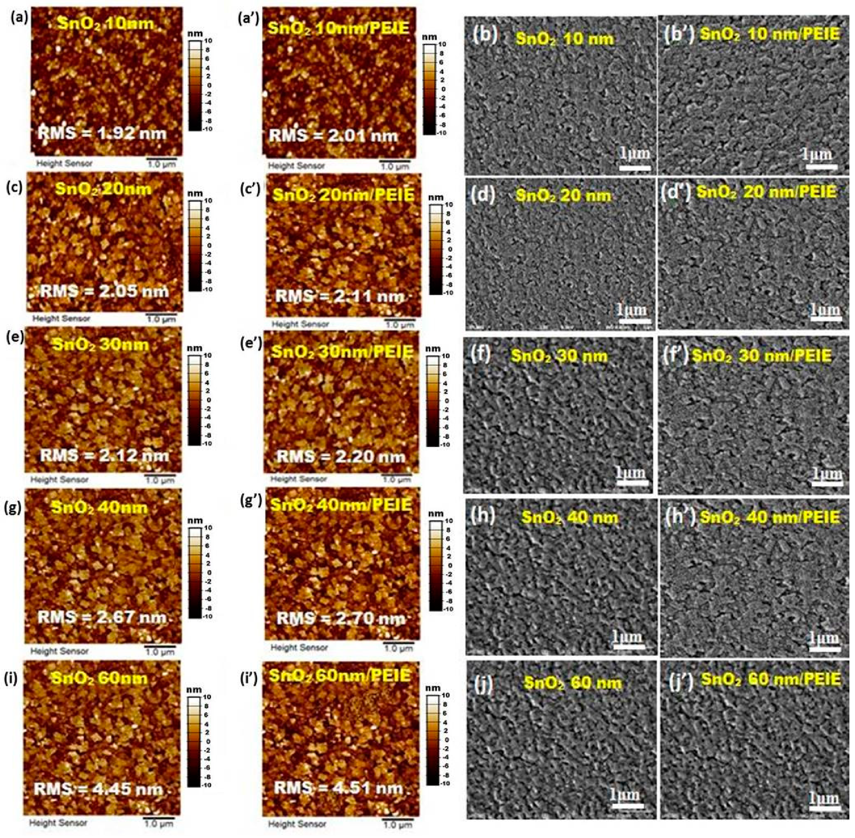
4.1.3. SEM and AFM Micrographs

In order to study the thickness effect on SnO2 surface morphology and topography as well as the film’s roughness, AFM and SEM images were recorded for different film thicknesses with and without PEIE on the ITO substrate, as illustrated in Figure 4.
One can see that the SnO2 film surface changed with thickness, and the surface morphology was rather homogeneous with surface RMS roughness (root mean square roughness) of 1.92, 2.05, 2.12, 2.67 and 4.45 nm, with an approximate error of 1%, for SnO2 films with thicknesses of 10, 20, 30, 40 and 60 nm, respectively without an ultrathin layer of PEIE. As can be seen from the AFM and SEM micrographs images, continuous films were formed on ITO substrates, and the nucleation process was completed and nucleus growth had already preceded. After PEIE deposition onto SnO2, AFM and SEM micrographs showed no agglomeration of PEIE on the surface and no significant changes compared to samples without PEIE.

4.1.4. Hall Effect Study

Hall effect measurement was performed to investigate electrical properties of SnO2 films with different thicknesses. The obtained parameters of bulk concentration (n), resistivity (ρ) and mobility (μ) are listed in Table 1. The electrical properties confirmed the n-type character of SnO2; moreover, the resistivity increased with SnO2 thickness, and the charge carrier concentration varied with the thickness and presented a maximum value at 20 nm.

4.2. Solar Cell Device Characterizations

4.2.1. XRD and GIXRD Study

The effect of PEIE at the SnO2/P3HT:PCBM interface was investigated through various structural, optical and electrical analyses in order to understand the buffer bilayer effect on inverted solar cell performance. XRD and GIXRD patterns of the prepared solar cells were based on the following structure: glass/ITO/SnO2/PEIE/P3HT:PCBM, as depicted in Figure 5a,b. Figure 5a reports the XRD patterns of the prepared solar cells with different SnO2 thicknesses (10, 20, 30, 40, and 60 nm). One can notice that the patterns demonstrated diffraction peaks corresponding to ITO, SnO2 and P3HT, suggesting a well-defined crystal structure of these materials. Diffraction peaks identifying polycrystalline structure of ITO were attributed to (211), (400) and (411) planes. Comparing the P3HT:PCBM blend diffractograms with that of pure P3HT (Figure 2), it was evidenced that the blend was characterized by (100), (200) and (300), which were attributed to the P3HT crystalline structure; the diffraction peak (100) at 2θ = 5.3° corresponded to the interchain spacing of 16.32 Å associated with inter-digitated alkyl [44]. The SnO2 diffraction pattern was dominated by the (110) peak positioned at 2θ~26.52° regardless of the SnO2 thickness. This peak, for all prepared devices with different SnO2 thicknesses, was an indication of the well-textured growth of SnO2 by sputtering [45].
The elaborated devices were characterized by XRD and GIRXD using an incident angle of 0.5° (Figure 5b) to localize all the peaks attributed to SnO2; the main peak of the latter was positioned at 2θ~26.52° and was attributed to the (110) plane; these patterns exhibited another weak peak at 2θ~25° that belonged to the SnOx orthorhombic phase (in accordance with JCPDS card no. 00-013-0111). Moreover, the GIXRD patterns revealed an increase in the peak intensity corresponding to the SnO2 tetragonal phase by increasing SnO2 thickness from 10 to 60 nm, which became sharper with a slight shift with respect to the JCPDS card; therefore, the crystallinity improved as well. This indicates that SnO2 surface morphology depends on SnO2 thickness, which was also proven by SEM and AFM images.

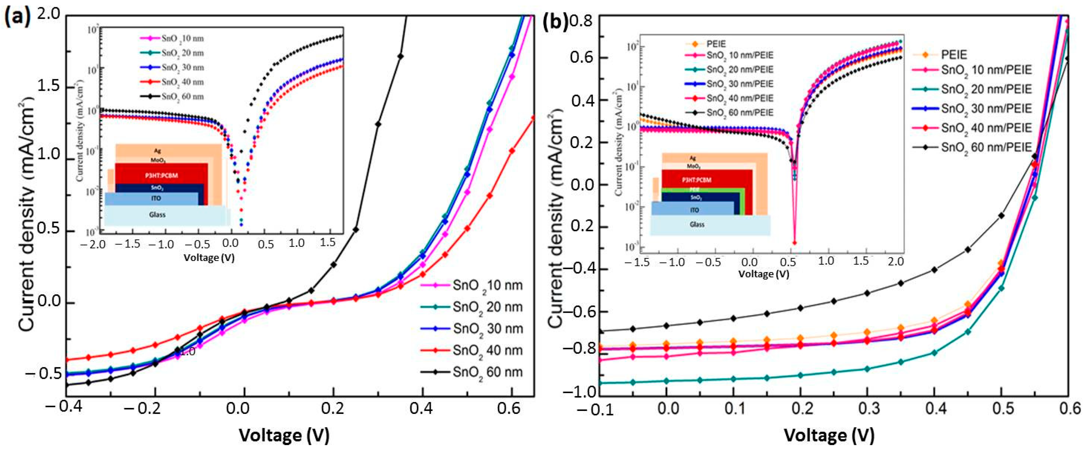
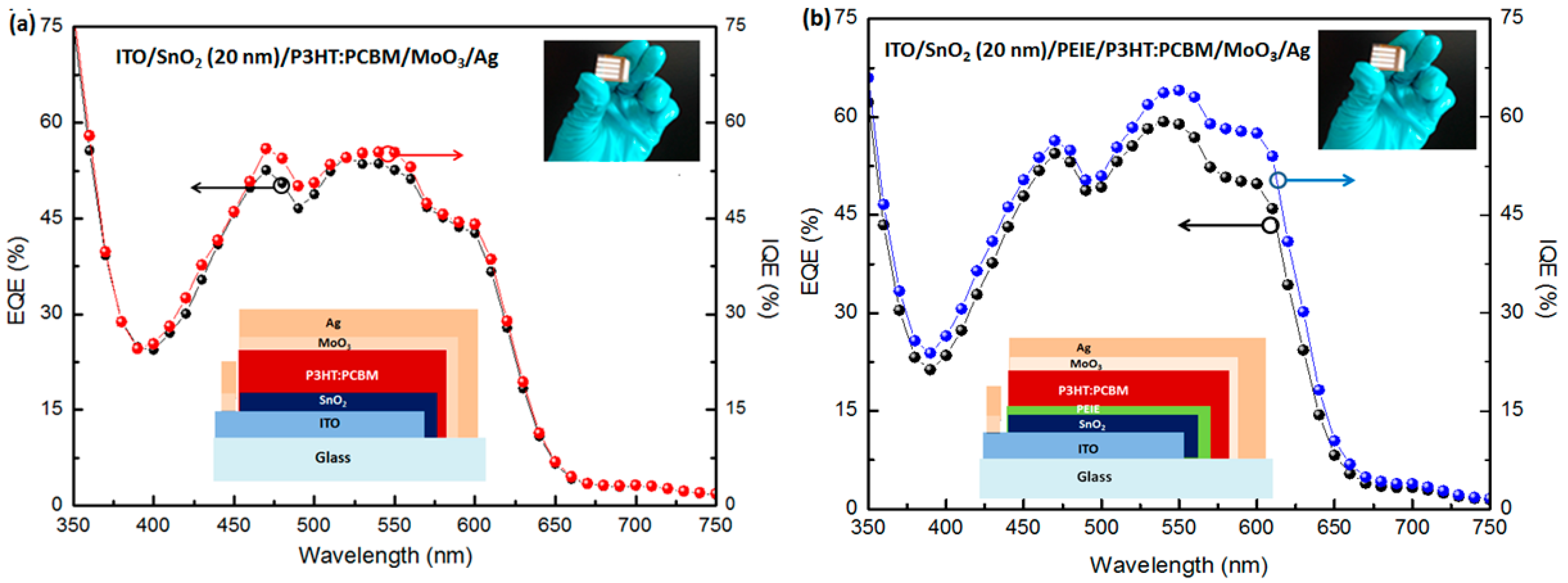
4.2.2. J–V Characterization and EQE Measurements

The metrics parameters of the elaborated inverted organic solar cells with and without PEIE were extracted from the current density–voltage (J–V) characteristics under illumination using AM1.5G with an irradiance of 100 mW/cm2. The determined parameters are summarized in Table 2, displaying short-circuit current density (JSC), open-circuit voltage (VOC), fill factor (FF) and power conversion efficiency (PCE).
The J–V characteristics of glass/ITO/SnO2/P3HT:PCBM/MoO3/Ag inverted solar cells based on SnO2 exhibited lower efficiencies (see Figure 6a). These low efficiencies were due to the high work function (WF) of SnO2 that prevented charge carrier mobility, which interrupted charge transfer from the active layer to SnO2 and/or charge trapping by interfacial ITO/SnO2 and SnO2/P3HT:PCBM. In order to enhance the performance of these devices, the surface modifier PEIE was introduced on top of SnO2 to elaborate a cathode bilayer device with the configuration ITO/SnO2/PEIE/P3HT:PCBM/MoO3/Ag while maintaining a constant thickness of PEIE (≈ 10 nm) and changing SnO2 thickness (10, 20, 30, 40 and 60 nm).
The J–V characteristics for the elaborated devices with and without PEIE are depicted in Figure 6. The inverted organic solar cells with an SnO2/PEIE cathode bilayer demonstrated better performance compared to those without PEIE; the device with 20 nm thickness of SnO2 showed the highest performance with a short-circuit current density JSC = 7.86 mA.cm−2, an open-circuit voltage Voc = 570 mV, a fill factor FF = 63.5% and a power conversion efficiency PCE = 2.84%. The use of SnO2/PEIE as a cathode bilayer increased the device parameters compared to those obtained for devices with a single PEIE or SnO2 cathode layer only; the extracted photovoltaic parameters of the elaborated cells are presented in Table 2.
The incorporation of the PEIE layer improved the interface quality as well as enhanced charge collection ability, which revealed an improvement of the photovoltaic performance [46,47].
The difference in device performance, with different electron transport layers, was mostly due to the increase or decrease in the short circuit current densities, which were consistent with external quantum efficiency (EQE) measurements. The EQE is defined as number of charges (Ne) extracted at the electrodes divided by the number of photons (Nph) of a certain incident wavelength on the solar cell.
E Q E ( λ ) = N e N p h ( λ )
The external quantum efficiency and internal quantum efficiency spectra of the best 20 nm device of SnO2 with/without the PEIE layer are depicted in Figure 7a,b. These spectra exhibited broad and high spectral responses ranging from 400 to 600 nm. The best device with SnO2 (20 nm)/PEIE exhibited a maximum of 60% and 64% for EQE and IQE, respectively, around 550 nm. The device with only SnO2 showed maxima of 55% and 53% for EQE and IQE, respectively, around 550 nm. The best performing device with combined layers of SnO2 (20 nm) and PEIE was attributed to the well-aligned dipoles of PEIE on top of the SnO2 layer.

5. Conclusions

In this work, we demonstrated an efficiency enhancement of inverted organic solar cells based on heterojunction by combining aqueous solution processed PEIE and sputtered SnO2 as a cathode buffer bilayer by overcoming the limitations using a single cathode buffer layer and tuning the work function of ITO. The PEIE surface modifier within the sputtered SnO2 layer is a promising alternative buffer bilayer to maximize the percolation of electron charge carriers by the formation of a thin interfacial dipole between the electron-transporting layer ITO/SnO2 and the LUMO of PCBM. This facilitates electron transport to the electrode by lowering the energy barrier between the active layer and the ITO/SnO2 interface, and by suppressing trap-assisted recombination, as well as improving the wettability between these layers, which leads to increases in the short-circuit current density and the fill factor. The optimization of SnO2 deposition parameters led to a highly efficient device using the following structure: ITO/SnO2 (20nm)/PEIE/P3HT:PCBM/MoO3/Ag. An increase from 0.08% for a single buffer layer up to 2.84% using the SnO2 (20 nm)/PEIE cathode buffer bilayer was obtained.

Author Contributions

I.A. performed the experiments and the fabrication and characterization of the devices, as well as the discussion of the results and wrote the manuscript. S.A. supervised the work and helped in the discussion and interpretation of the results besides, she contributed in the writing of the paper and revised the manuscript, with contributions from all authors. G.S. supervised the experiment and performed the electrical measurement of the devices and contributed to the structural characterization of the solar cells, besides, G.S. contributed in the writing of the paper and revised the manuscript. S.R. helped with data analysis of the results and discussion. N.Z. contributed to the solar cell elaboration and electrical characterization of the devices. T.H. supervised the experimental work, conceived the work plan and revised the manuscript; G.F. optimized and prepares the SnO2 layers. A.S. and M.A.-L. contributed to the supervision of the work and revised the manuscript. A.D. and Z.S. conceived the idea, participated in the discussion of the results and supervised the work. All authors have read and agreed to the published version of the manuscript.

Funding

This research was funded by the MEFCRS PPR project Development of Organic Solar Cells, and the Erasmus+ MEDSOL program.

Acknowledgments

The authors are thankful to J. Bartringer and C. Leuvrey for providing technical assistance.

Conflicts of Interest

The authors declare no conflict of interest.

References

  1. Adhikari, N.; Khatiwada, D.; Dubey, A.; Qiao, Q. Device and morphological engineering of organic solar cells for enhanced charge transport and photovoltaic performance. J. Photonics Energy 2015, 5, 057207. [Google Scholar] [CrossRef] [Green Version]
  2. Ghosh, S.; Serrano, L.; Ebenhoch, B.; Rotello, V.; Cooke, G.; Samuel, I.D.W. Organic solar cells based on acceptor-functionalized diketopyrrolopyrrole derivatives. J. Photonics Energy 2015, 5, 057215. [Google Scholar] [CrossRef]
  3. Kim, H.; Shin, M.; Kim, Y. Distinct Annealing Temperature in Polymer:Fullerene:Polymer Ternary Blend Solar Cells. J. Phys. Chem. C 2009, 113, 1620–1623. [Google Scholar] [CrossRef]
  4. Song, M.; You, D.S.; Lim, K.; Park, S.; Jung, S.; Kim, C.S.; Kim, N.-H.; Kim, D.-G.; Kim, J.-K.; Park, J.; et al. Highly efficient and bendable organic solar cells with solution-processed silver nanowire electrodes. Adv. Funct. Mater. 2013, 23, 4177–4184. [Google Scholar] [CrossRef]
  5. Zhou, Z.; Liu, W.; Zhou, G.; Zhang, M.; Qian, D.; Zhang, J.; Chen, S.; Xu, S.; Yang, C.; Gao, F.; et al. Subtle molecular tailoring induces significant morphology optimization enabling over 16% efficiency organic solar cells with efficient charge generation. Adv. Mater. 2019, 32, 1906324. [Google Scholar] [CrossRef] [PubMed]
  6. Liu, L.; Kan, Y.; Gao, K.; Wang, J.; Zhao, M.; Chen, H.; Zhao, C.; Jiu, T.; Jen, A.-K.-Y.; Li, Y. Graphdiyne derivative as multifunctional solid additive in binary organic solar cells with 17.3% efficiency and high reproductivity. Adv. Mater. 2020, 32, e1907604. [Google Scholar] [CrossRef]
  7. Xiao, J.; Chen, Z.; Zhang, G.; Li, Q.-Y.; Yin, Q.; Huang, F.; Xu, Y.-X.; Yip, H.; Cao, Y.; Jiang, X. Efficient device engineering for inverted non-fullerene organic solar cells with low energy loss. J. Mater. Chem. C 2018, 6, 4457–4463. [Google Scholar] [CrossRef]
  8. Huang, J.; Li, C.-Z.; Chueh, C.-C.; Liu, S.-Q.; Yu, J.; Jen, A.K.-Y. 10.4% power conversion efficiency of ITO-free organic photovoltaics through enhanced light trapping configuration. Adv. Energy Mater. 2015, 5, 1500406. [Google Scholar] [CrossRef]
  9. Song, M.; Kang, J.W.; Kim, D.-H.; Kwon, J.-D.; Park, S.-G.; Nam, S.; Jo, S.; Ryu, S.Y.; Kim, C.S. Self-assembled monolayer as an interfacial modification material for highly efficient and air-stable inverted organic solar cells. Appl. Phys. Lett. 2013, 102, 143303. [Google Scholar] [CrossRef]
  10. Chochos, C.L.; Singh, R.; Gregoriou, V.G.; Kim, M.; Katsouras, A.; Serpetzoglou, E.; Konidakis, I.; Stratakis, E.; Cho, K.; Avgeropoulos, A. Enhancement of the power-conversion efficiency of organic solar cells via unveiling an appropriate rational design strategy in indacenodithiophene-alt-quinoxaline π-conjugated polymers. ACS Appl. Mater. Interfaces 2018, 10, 10236–10245. [Google Scholar] [CrossRef]
  11. Huang, C.; Liao, X.; Gao, K.; Zuo, L.; Lin, F.; Shi, X.; Li, C.-Z.; Liu, H.; Li, X.; Liu, F.; et al. highly efficient organic solar cells based on S,N-heteroacene non-fullerene acceptors. Chem. Mater. 2018, 30, 5429–5434. [Google Scholar] [CrossRef]
  12. Yan, C.; Barlow, S.; Wang, Z.; Yan, H.; Jen, A.K.-Y.; Marder, S.R.; Zhan, X. Non-fullerene acceptors for organic solar cells. Nat. Rev. Mater. 2018, 3, 18003. [Google Scholar] [CrossRef]
  13. Xie, Y.; Yang, F.; Li, Y.; Uddin, M.A.; Bi, P.; Fan, B.; Cai, Y.; Hao, X.-T.; Woo, H.Y.; Li, W.; et al. Morphology control enables efficient ternary organic solar cells. Adv. Mater. 2018, 30, 1803045. [Google Scholar] [CrossRef] [PubMed]
  14. Song, X.; Gasparini, N.; Ye, L.; Yao, H.; Hou, J.; Ade, H.; Baran, D. Controlling blend morphology for ultrahigh current density in nonfullerene acceptor-based organic solar cells. ACS Energy Lett. 2018, 3, 669–676. [Google Scholar] [CrossRef]
  15. Kaur, N.; Singh, M.; Pathak, D.; Wagner, T.; Nunzi, J.-M. Organic materials for photovoltaic applications: Review and mechanism. Synth. Met. 2014, 190, 20–26. [Google Scholar] [CrossRef]
  16. Choi, H.; Mai, C.-K.; Kim, H.-B.; Jeong, J.; Song, S.; Bazan, G.C.; Kim, J.Y.; Heeger, A.J. Conjugated polyelectrolyte hole transport layer for inverted-type perovskite solar cells. Nat. Commun. 2015, 6, 7348. [Google Scholar] [CrossRef] [Green Version]
  17. Lim, T.; Kim, C.; Song, M.; Ryu, S.Y.; Ju, S. Organic solar cells with surface-treated graphene thin film as interfacial layer. Synth. Met. 2015, 205, 1–5. [Google Scholar] [CrossRef]
  18. Yin, Z.; Wei, J.; Zheng, Q. Interfacial Materials for Organic Solar Cells: Recent Advances and Perspectives. Adv. Sci. 2016, 3, 1500362. [Google Scholar] [CrossRef] [Green Version]
  19. Liao, W.-P.; Wu, J.-J. Efficient electron collection in hybrid polymer solar cells: In-situ-generated ZnO/Poly(3-hexylthiophene) scaffolded by a TIO2 nanorod array. J. Phys. Chem. Lett. 2013, 4, 1983–1988. [Google Scholar] [CrossRef]
  20. Jouane, Y.; Schmerber, G.; Heiser, T.; Chapuis, Y.-A.; Colis, S.; Kern, P.; Dinia, A. Room temperature ZnO growth by rf magnetron sputtering on top of photoactive P3HT: PCBM for organic solar cells. J. Mater. Chem. 2011, 21, 1953–1958. [Google Scholar] [CrossRef]
  21. Yang, H.; Zhu, S.; Pan, N. Studying the mechanisms of titanium dioxide as ultraviolet-blocking additive for films and fabrics by an improved scheme. J. Appl. Polym. Sci. 2004, 92, 3201–3210. [Google Scholar] [CrossRef]
  22. Wang, J.-C.; Weng, W.-T.; Tsai, M.-Y.; Lee, M.-K.; Horng, S.-F.; Perng, T.-P.; Kei, C.-C.; Yu, C.-C.; Meng, H.-F. Highly efficient flexible inverted organic solar cells using atomic layer deposited ZnO as electron selective layer. J. Mater. Chem. 2010, 20, 862–866. [Google Scholar] [CrossRef] [Green Version]
  23. Tran, V.-H.; Eom, S.H.; Yoon, S.C.; Kim, S.-K.; Lee, S.-H. Enhancing device performance of inverted organic solar cells with SnO2/Cs2CO3 as dual electron transport layers. Org. Electron. 2019, 68, 85–95. [Google Scholar] [CrossRef]
  24. Hu, Z.; Zhang, J.; Hao, Z.; Hao, Q.; Geng, X.; Zhao, Y. Highly efficient organic photovoltaic devices using F-doped SnO2 anodes. Appl. Phys. Lett. 2011, 98, 123302. [Google Scholar] [CrossRef]
  25. Yang, F.; Forrest, S.R. Organic Solar Cells Using Transparent SnO2–F Anodes. Adv. Mater. 2006, 18, 2018–2022. [Google Scholar] [CrossRef]
  26. Huang, S.; Tang, Y.; Dang, Y.; Xu, X.; Dong, Q.; Kang, B.; Silva, S. Low-temperature solution-processed mg:sno2 nanoparticles as an effective cathode interfacial layer for inverted polymer solar cell. ACS Sustain. Chem. Eng. 2018, 6, 6702–6710. [Google Scholar] [CrossRef]
  27. Tran, V.-H.; Khan, R.; Lee, I.-H.; Lee, S.-H. Low-temperature solution-processed ionic liquid modified SnO2 as an excellent electron transport layer for inverted organic solar cells. Sol. Energy Mater. Sol. Cells 2018, 179, 260–269. [Google Scholar] [CrossRef]
  28. Huang, S.; Tang, Y.; Yu, A.; Wang, Y.; Shen, S.; Kang, B.; Silva, S.; Lu, G. Solution-processed SnO2 nanoparticle interfacial layers for efficient electron transport in ZnO-based polymer solar cells. Org. Electron. 2018, 62, 373–381. [Google Scholar] [CrossRef]
  29. Jin, W.-Y.; Ginting, R.T.; Jin, S.-H.; Kang, J.-W. Highly stable and efficient inverted organic solar cells based on low-temperature solution-processed PEIE and ZnO bilayers. J. Mater. Chem. A 2016, 4, 3784–3791. [Google Scholar] [CrossRef]
  30. Zhou, Y.; Fuentes-Hernandez, C.; Shim, J.W.; Khan, T.M.; Kippelen, B. High performance polymeric charge recombination layer for organic tandem solar cells. Energy Environ. Sci. 2012, 5, 9827–9832. [Google Scholar] [CrossRef]
  31. Udum, Y.; Denk, P.; Adam, G.; Apaydin, D.H.; Nevosad, A.; Teichert, C.; White, M.; Sariciftci, N.S.; Scharber, M.C. Inverted bulk-heterojunction solar cell with cross-linked hole-blocking layer. Org. Electron. 2014, 15, 997–1001. [Google Scholar] [CrossRef] [PubMed] [Green Version]
  32. Lee, W.; Jung, J.W. High performance polymer solar cells employing a low-temperature solution-processed organic–inorganic hybrid electron transport layer. J. Mater. Chem. A 2016, 4, 16612–16618. [Google Scholar] [CrossRef]
  33. Lim, K.-G.; Ahn, S.; Lee, T.-W. Energy level alignment of dipolar interface layer in organic and hybrid perovskite solar cells. J. Mater. Chem. C 2018, 6, 2915–2924. [Google Scholar] [CrossRef]
  34. Venkatesan, S.; Ngo, E.; Khatiwada, D.; Zhang, C.; Qiao, Q. Enhanced Lifetime of Polymer Solar Cells by Surface Passivation of Metal Oxide Buffer Layers. ACS Appl. Mater. Interfaces 2015, 7, 16093–16100. [Google Scholar] [CrossRef] [PubMed]
  35. Zhou, Y.; Fuentes-Hernandez, C.; Shim, J.; Meyer, J.; Giordano, A.J.; Li, H.; Winget, P.; Papadopoulos, T.A.; Cheun, H.; Kim, J.; et al. A universal method to produce low-work function electrodes for organic electronics. Science 2012, 336, 327–332. [Google Scholar] [CrossRef]
  36. Courtright, B.A.E.; Jenekhe, S.A. Polyethylenimine Interfacial Layers in Inverted Organic Photovoltaic Devices: Effects of Ethoxylation and Molecular Weight on Efficiency and Temporal Stability. ACS Appl. Mater. Interfaces 2015, 7, 26167–26175. [Google Scholar] [CrossRef]
  37. Bouras, K.; Schmerber, G.; Rinnert, H.; Aureau, D.; Park, H.; Ferblantier, G.; Colis, S.; Fix, T.; Park, C.; Kim, W.K.; et al. Structural, optical and electrical properties of Nd-doped SnO2 thin films fabricated by reactive magnetron sputtering for solar cell devices. Sol. Energy Mater. Sol. Cells 2016, 145, 134–141. [Google Scholar] [CrossRef]
  38. Bouras, K.; Schmerber, G.; Aureau, D.; Rinnert, H.; Ferblantier, G.; Fix, T.; Colis, S.; Bazylewski, P.; Leedahl, B.; Etcheberry, A.; et al. Insight into photon conversion of Nd 3+ doped low temperature grown p and n type tin oxide thin films. RSC Adv. 2016, 6, 67157–67165. [Google Scholar] [CrossRef]
  39. Tran, V.-H.; Ambade, R.B.; Ambade, S.; Lee, S.-H.; Lee, I.H. Low-temperature solution-processed SnO2 nanoparticles as a cathode buffer layer for inverted organic solar cells. ACS Appl. Mater. Interfaces 2017, 9, 1645–1653. [Google Scholar] [CrossRef]
  40. Chu, C.-W.; Yang, H.; Hou, W.-J.; Huang, J.; Li, G.; Yang, Y. Control of the nanoscale crystallinity and phase separation in polymer solar cells. Appl. Phys. Lett. 2008, 92, 103306. [Google Scholar] [CrossRef] [Green Version]
  41. Seidler, N.; Lazzerini, G.M.; Destri, G.L.; Marletta, G.; Cacialli, F. Enhanced crystallinity and film retention of P3HT thin-films for efficient organic solar cells by use of preformed nanofibers in solution. J. Mater. Chem. C 2013, 1, 7748. [Google Scholar] [CrossRef] [Green Version]
  42. Müllerová, J.; Kaiser, M.; Nadazdy, V.; Siffalovic, P.; Majkova, E. Optical absorption study of P3HT:PCBM blend photo-oxidation for bulk heterojunction solar cells. Sol. Energy 2016, 134, 294–301. [Google Scholar] [CrossRef]
  43. Li, L.; Lu, G.; Yang, X. Improving performance of polymer photovoltaic devices using an annealing-free approach via construction of ordered aggregates in solution. J. Mater. Chem. 2008, 18, 1984. [Google Scholar] [CrossRef]
  44. Kanai, K.; Miyazaki, T.; Suzuki, H.; Inaba, M.; Ouchi, Y.; Seki, K. Effect of annealing on the electronic structure of poly(3-hexylthiophene) thin film. Phys. Chem. Chem. Phys. 2010, 12, 273–282. [Google Scholar] [CrossRef] [PubMed]
  45. Yu, S.; Yang, W.; Li, L.; Zhang, W. Improved chemical stability of ITO transparent anodes with a SnO2 buffer layer for organic solar cells. Sol. Energy Mater. Sol. Cells 2016, 144, 652–656. [Google Scholar] [CrossRef]
  46. Goo, J.S.; Shin, S.-C.; You, Y.-J.; Shim, J.W. Polymer surface modification to optimize inverted organic photovoltaic devices under indoor light conditions. Sol. Energy Mater. Sol. Cells 2018, 184, 31–37. [Google Scholar] [CrossRef]
  47. Ha, J.; Kim, H.; Lee, H.; Lim, K.-G.; Lee, T.-W.; Yoo, S. Device architecture for efficient, low-hysteresis flexible perovskite solar cells: Replacing TiO2 with C60 assisted by polyethylenimine ethoxylated interfacial layers. Sol. Energy Mater. Sol. Cells 2017, 161, 338–346. [Google Scholar] [CrossRef]
Figure 1. (a) Schematic structure of the inverted hybrid solar cell. (b) Cross-sectional SEM figure of device used in this study. (c) Chemical structure of P3HT, PCBM and PEIE. (d) Energy level diagram of the inverted hybrid solar cells investigated in this work.
Crystals 10 00731 g001
Figure 2. X-ray diffraction patterns of (a) sputtered SnO2 deposited on quartz substrate and (b) P3HT spin-coated on glass substrate.
Crystals 10 00731 g002
Figure 3. (a) Absorption spectra of P3HT:PCBM deposited on glass substrate and (b) transmittance spectra of SnO2 with different thicknesses deposited on quartz substrate.
Crystals 10 00731 g003
Figure 4. The 2D-AFM and SEM micrographs of sputtered SnO2 without PEIE for 10 nm (a,b), 20 nm (c,d), 30 nm (e,f), 40 nm (g,h), 60 nm (i,j) and with PEIE coated on SnO2 10 nm (a’,b’), 20 nm (c’,d’), 30 nm (e’,f’), 40 nm (g’,h’) and 60 nm (i’,j’).
Crystals 10 00731 g004
Figure 5. XRD (a) and GIXRD (b) patterns of all device glass/ITO/SnO2/PEIE/P3HT:PCBM/MoO3/Ag structures with different thicknesses of SnO2 (10, 20, 30, 40, 60 nm).
Crystals 10 00731 g005
Figure 6. J–V characteristics of glass/ITO/SnO2/P3HT:PCBM/MoO3/Ag (a) and glass/ITO/SnO2/PEIE/P3HT:PCBM/MoO3/Ag; (b) devices with different thicknesses of SnO2 (10, 20, 30, 40, 60 nm).
Crystals 10 00731 g006
Figure 7. EQE and IQE curve of (a) the device with only-SnO2 (20 nm) and (b) best cell based on glass/ITO/SnO2 20 nm)/PEIE ETL.
Crystals 10 00731 g007
Table 1. Hall effect measurements of sputtered SnO2 deposited on quartz.
Samplesn (1020cm−3)ρ (10−3Ω·cm)μ (cm2/V·s)
10 nm−1.83 ± 0.031.87 ± 0.024.72 ± 0.02
20 nm−2.62 ± 0.021.78 ± 0.0311.12 ± 0.02
30 nm−2.13 ± 0.045.54 ± 0.024.70 ± 0.03
40 nm−2.15 ± 0.036.24 ± 0.044.30 ± 0.02
60 nm−1.78 ± 0.028.33 ± 0.024.20 ± 0.03
Table 2. Characteristics of P3HT:PCBM-based bulk heterojunction devices with different electron transporting layer.
ETLsThickness of SnO2 (nm)JSC * (mA/cm2)VOC * (V)FF * (%)PCE * (%)
SnO2201.25 ± 0.100.22 ± 0.0530.0 ± 0.90.08 ± 0.10
PEIE-6.25 ± 0.090.55 ± 0.0155.8 ± 0.41.91 ± 0.07
SnO2/PEIE107.08 ± 0.020.56 ± 0.0163.1 ± 0.82.50 ± 0.07
207.86 ± 0.050.57 ± 0.0263.5 ± 0.52.84 ± 0.04
306.55 ± 0.010.56 ± 0.0166.6 ± 0.62.44 ± 0.04
406.54 ± 0.020.56 ± 0.0166.3 ± 0.62.42 ± 0.06
605.60 ± 0.010.55 ± 0.0342.8 ± 0.71.31 ± 0.02
* The averaged values were calculated from 8 solar cells.

