1. Introduction
The progressive availability of an expanding range of semiconductor heterojunctions over the second part of the last century has paved the way to many of the present key devices for electronics and opto-electronics. Today, all light-emitting diodes (LEDs) and laser diodes, together with the highest-performance microwave transistors and photodetectors, include at least one such heterojunction and there is a strong motivation in further extending the range of functional heterojunctions available for the design and manufacturing of new higher-performance devices.
Still, all the heterojunctions used today within the active parts of successful devices are isogenic heterojunctions, meaning that both semiconductor materials belong to the same chemical family, such as Group IV, III-V or II-VI. Attempts have been made to use exogenic quasi-matched heterojunctions such as GaP/Si [
1], GaAs/Ge [
2] or ZnSe/GaAs [
3], or highly mismatched ones such as GaN/SiC [
4], but with no real technological breakthrough.
One possible reason is that for such exogenic heterojunctions every single chemical element of each semiconductor material can behave as a doping element within the other material. Therefore, any diffusion of chemical elements from one material into the other can dramatically change the doping profile and subsequently the electric field profile within the heterostructure.
The usual methods to synthesize high quality functional heterojunctions involves epitaxy processes such as Molecular Beam Epitaxy (MBE) or Chemical Vapor Deposition (CVD), with a substrate surface at a high temperature in order to get high enough atomic surface mobility. This high temperature may favor diffusion in exogenic heterojunctions. However, it has already been demonstrated that atomic layer deposition/epitaxy (ALD/ALE) does not require such high temperatures to provide epitaxial ordering at the hetero-interface. Therefore, the use of a ALE process is of interest to synthesize such exogenic heterostructures.
ZnO is a wide-bandgap semiconductor with a hexagonal würtzite crystal structure (2H) similar to that of GaN and close to the hexagonal structure of 4H-SiC. Today, it is used mainly for its piezoelectric properties in electro-acoustic transducers, and, also, polycrystalline ZnO is the active material of widely used protection devices such as varistors. Still, despite some results reported on isogenic MgZnO/ZnO heterostructures [
5], no successful heterojunction device based on ZnO has yet reached the industrial stage.
This paper reports on a preliminary work which can be considered as a first step towards a future demonstration of new functional exogenic heterojunctions between two wide-bandgap compound semiconductors: on one side ZnO, which belongs to the II-VI family, and, on the other side, either the III-V GaN or the group IV 4H-SiC. In particular, GaN and 4H-SiC have been chosen because they are presently the most mature wide-bandgap semiconductor materials and the first that have already reached the industrial stage for the mass production of devices for opto-electronics and power electronics.
2. Materials and Methods
2.1. GaN and SiC Samples
Starting GaN samples are pieces of Metal-Organic Chemical Vapor Deposition (MOCVD) hetero-epitaxial structures of GaN on sapphire substrates with on-axis c-orientation. The top surface of the GaN has [0001] orientation with Ga polarity. Before the ZnO deposition, the GaN is cleaned using diluted HCl.
Starting 4H-SiC samples are pieces of commercial n-type doped substrates with 4° off (0001) orientation and Si polarity. Before ALD deposition of ZnO, the samples are deoxidized in diluted HF.
2.2. ALD Reactor
The depositions took place in a home-made continuous flow cold-wall horizontal quartz reactor. A non-conventional infrared heating system was used, allowing fast heating and cooling. Metal precursor and water were introduced alternatively sequentially by pneumatic ALD valves from their respective reservoirs. The sample holder is made of graphite and was heated through the quartz wall by an infrared lamp. A thermocouple placed in the middle top of the holder ensured temperature control of the substrates.
2.3. Precursors
Di-Ethyl-Zinc (DEZn) was used as zinc precursor due to its adequate chemical reactivity and vapor pressure range. DEZn is the most popular Zn source, for both MOCVD [
6] and ALD [
7]. It is conditioned in a stainless steel container kept at 25 °C. High-purity Milli-Q deionized water, also conditioned in a stainless steel container kept at room temperature, was employed as oxygen source.
2.4. ALD Process
Purified argon was used as carrier and purge during the process. Each deposition started with a purge stage, before the ALD cycles. The Zn precursor was first introduced, followed by a pulse of H2O. Both precursors were kept separate to each other by purge steps, ensuring self-limited surface reaction. The four elementary steps were repeated until reaching the desired film thickness. The deposition took place in a temperature range of 180–250 °C in continuous flow. An opening time of 0.3 s followed by a purge of 15 s were set for both precursors. For the deposition, pure argon was used as a carrier and purge gas at a constant flow rate of 200 sccm with a total pressure inside the reactor of 1 mbar. As a function of the deposition temperature, the growth per cycle ranges from 0.13 to 0.25 nm. Adjusting the number of cycles performed, layers with thicknesses from 20 to 100 nm were investigated.
2.5. Characterizations
The thickness of the deposited ZnO was measured using ellipsometry (Sopra, Paris, France). A modified Cauchy model was employed to fit the obtained curves. This measurement technique was first benchmarked on a few samples using both X-ray reflectivity and atomic force microscopy (AFM) (Scientec, Les Ullis, France) on steps obtained by masking or lithography.
Scanning electron microscopy (SEM) was performed at 20 kV on top of the samples using a Quanta 250 FEG FEI microscope (FEI, Hillsboro, OR, USA). Transmission electron microscopy (TEM) images were recorded at 200 kV from cross-sections on copper TEM grids using a Jeol 2100F microscope (Jeol, Tokyo, Japan). Thin cross-sections have been realized by mechanical abrasion using diamond lapping disk down to a thickness of approximately 50 µm. They were then further thinned using an ion beam at grazing angle (6° to 8°) using a GATAN Precision Ion Polishing System (PIPSTM) model 691 (Gatan, Pleasanton, CA, USA).
Crystallinity was investigated by X-ray diffraction (XRD) using PAN Analytical and Rigaku Smartlab diffractometers (PAN Analytical, Almelo, the Netherlands; Rigaku, Tokyo, Japan). X-ray pole figures were performed at 2θ = 36.17° and 37°, corresponding to the (101) reflection of GaN and ZnO, respectively.
3. Results
3.1. ALD Growth of ZnO on Amorphous Silicon Oxide Surface
As a first step, ALD growth of ZnO was performed at temperatures ranging from 180–250 °C on an amorphous native silicon oxide surface of a silicon reference substrate. Subsequently, ALD growth was studied on single-crystal seeding surfaces.
It can be noted that no significant and reproducible ALD growth of ZnO obtained on the deoxidized silicon substrate using a diluted HF etch, regardless of the (100) or (111) orientation of the surface. This is fully coherent with all previous reports on ALD growth of ZnO using similar surfaces and growth conditions [
8], as anchors are required to initiate the growth.
All the deposited ZnO layers on native SiO
2 exhibit preferential orientation trends towards one or two crystallographic directions, as identified by X-ray diffraction (
Figure 1a). In all cases, (0001) is the dominant growth direction. Depending on the substrate temperature, (10-10) and (10-11) peaks can also be clearly identified. A higher substrate temperature favors ZnO texturing along (0001), as previously reported [
7].
The bright field TEM image, presented in
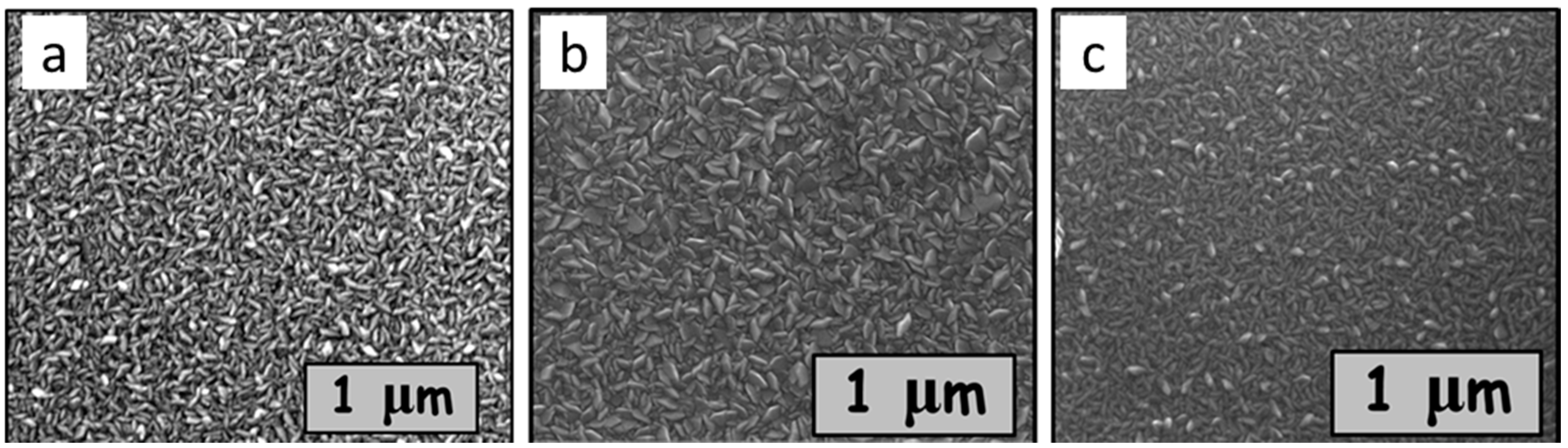
Figure 1b, shows the columnar structure of the ZnO layer. Dark field images (not presented here) confirm the high mosaicity of the in-plane orientation of the ZnO columns, which is also evidenced in the SEM images presented in
Figure 2a.
3.2. ALD Growth of ZnO on Surfaces of Highly Mismatched Single-Crystal GaAs and InP
GaAs and InP have both a sphalerite crystal structure with on-axis (111) surface topology similar to that of the on-axis (0001) ZnO surfaces of the same polarity.
ZnO layers grown at 250 °C onto GaAs (111B) and InP on-axis (111A) surfaces exhibit similar morphology as layers grown onto amorphous silicon oxide, as can be seen in
Figure 2b,c. Numerous trials of different cleaning procedures before ALD growth, using either alcohols and/or several inorganic acids or bases, did not bring any significant improvement of the final surface morphology. The deposition temperature was set at 250 °C in order to favor growth along the
c axis. No higher temperature was studied, to avoid damaging the substrates.
3.3. ALD Growth of ZnO onto GaN (0001-Ga) Surfaces
ALD growth on GaN (0001-Ga) surfaces yields ZnO layers with a very different structure and morphology compared to the previous substrates.
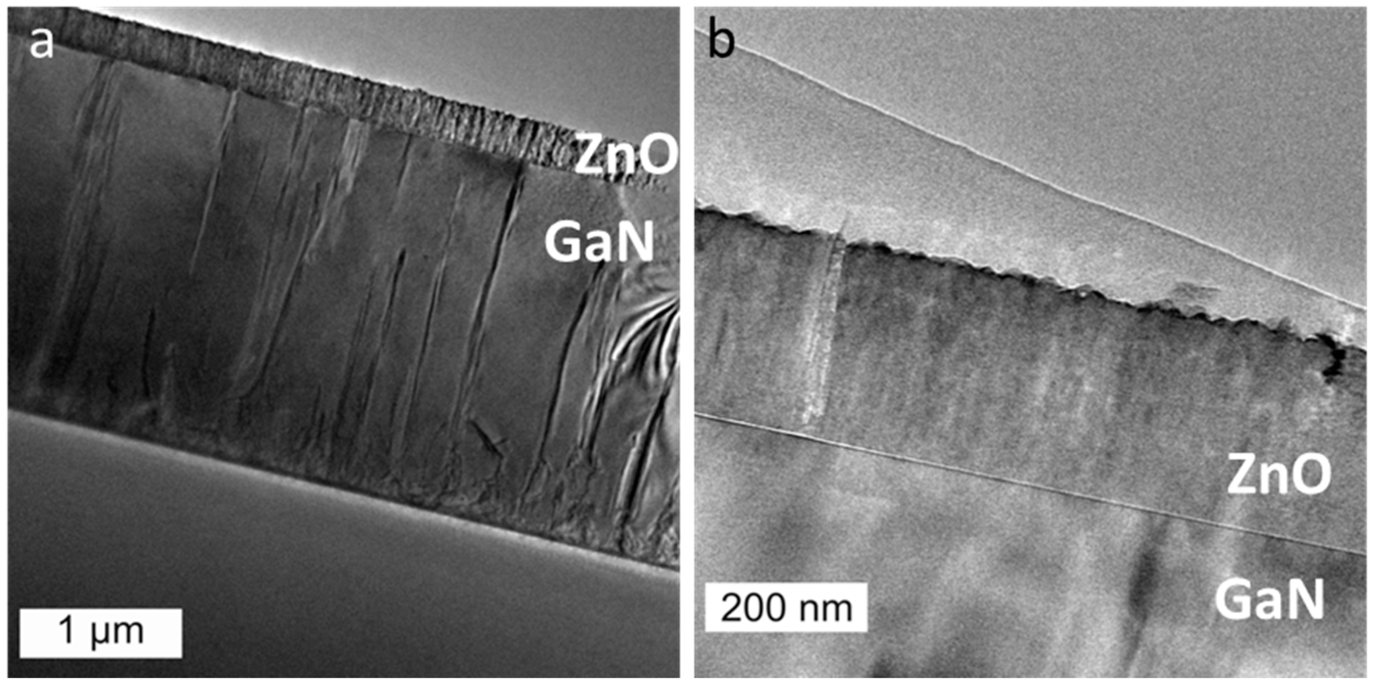
TEM images and selected area electron diffraction, as shown in
Figure 3 and
Figure 4, demonstrate an epitaxial ordering of ZnO onto the GaN seed at microscopic scale even at a deposition temperature as low as 180 °C.
The low-magnification image (
Figure 3a) reveals typical defects of the hetero-epitaxial GaN seeding layer as well as the columnar sub-structure of the ZnO layer.
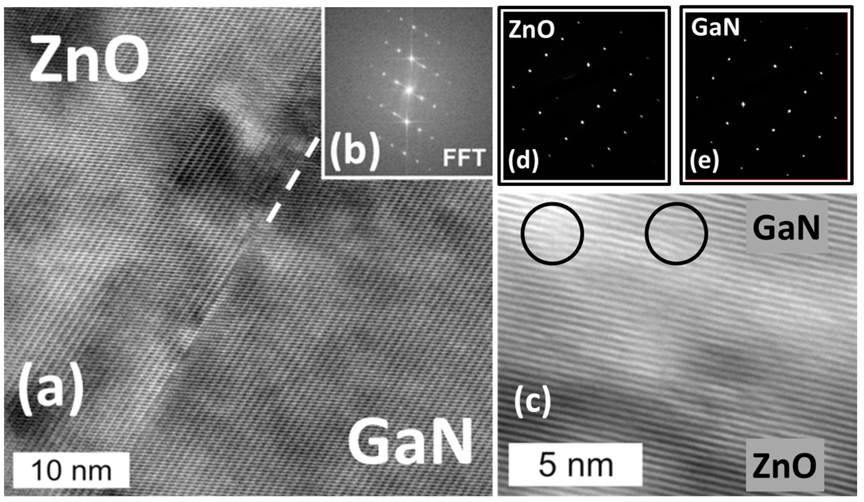
The high-magnification images (
Figure 4a,c) do not reveal evidence of the intermediate phase present between the GaN and ZnO, nor any doping-induced contrast close to the interface between the ZnO and GaN layers.
The regular stacking observed at high magnification in
Figure 4a,c confirms the epitaxial growth of ZnO onto GaN, and similar electron diffraction patterns, shown in
Figure 4d,e, confirm similar crystal systems and lattice parameters.
Figure 4c exhibits possible evidence for basal dislocations located close to the hetero-interface.
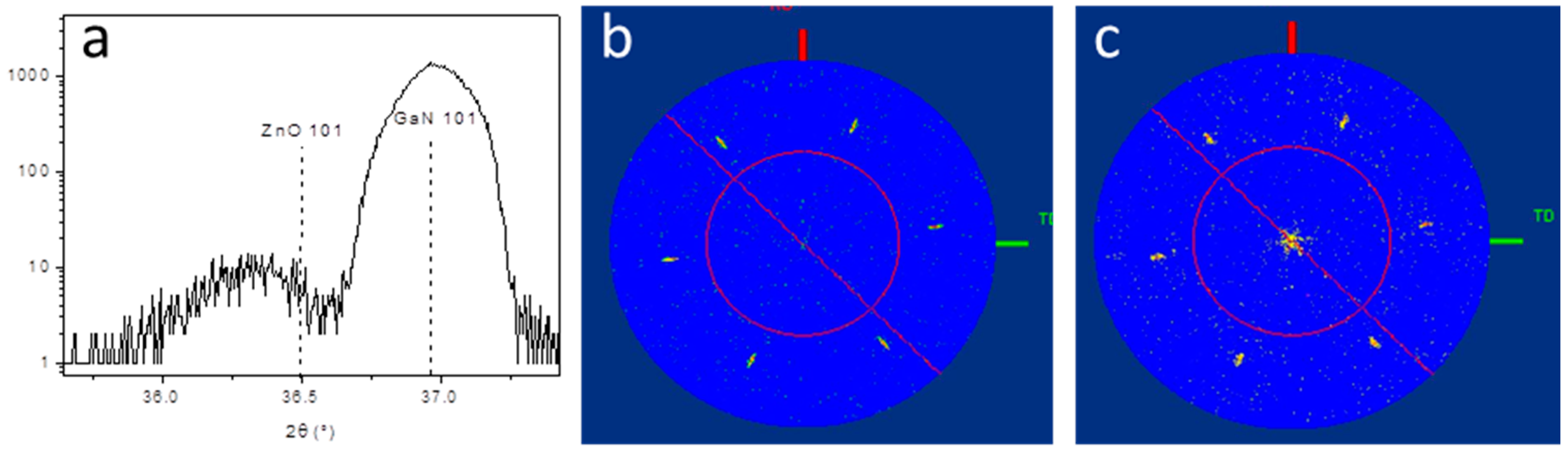
The (0002) X-ray diffraction does not allow clear separation of the GaN- and ZnO-related peaks, due to their close proximity. The high-resolution diffraction rocking curve, centered around the (101) peaks, (which are the same as the (10-11) ones as designated in 4-indexes notation), shown in
Figure 5b, exhibits well-separated ZnO and GaN peaks. The ZnO peak is clearly shifted towards lower angles, corresponding to a larger
c parameter, indicating a compressive a-plane stress compatible with pseudomorphic growth onto a relaxed GaN surface. Comparative pole figures were recorded from the GaN and ZnO (101) planes (
Figure 5a,c). A similar in-plane orientation and small mosaicity was demonstrated at the macroscopic scale for both the GaN seeding layer and the ALD-grown ZnO layer.
At this stage, all the experimental evidence is coherent with compressive pseudomorphic epitaxial growth of the ZnO onto the GaN seed, which is in line with the expectations.
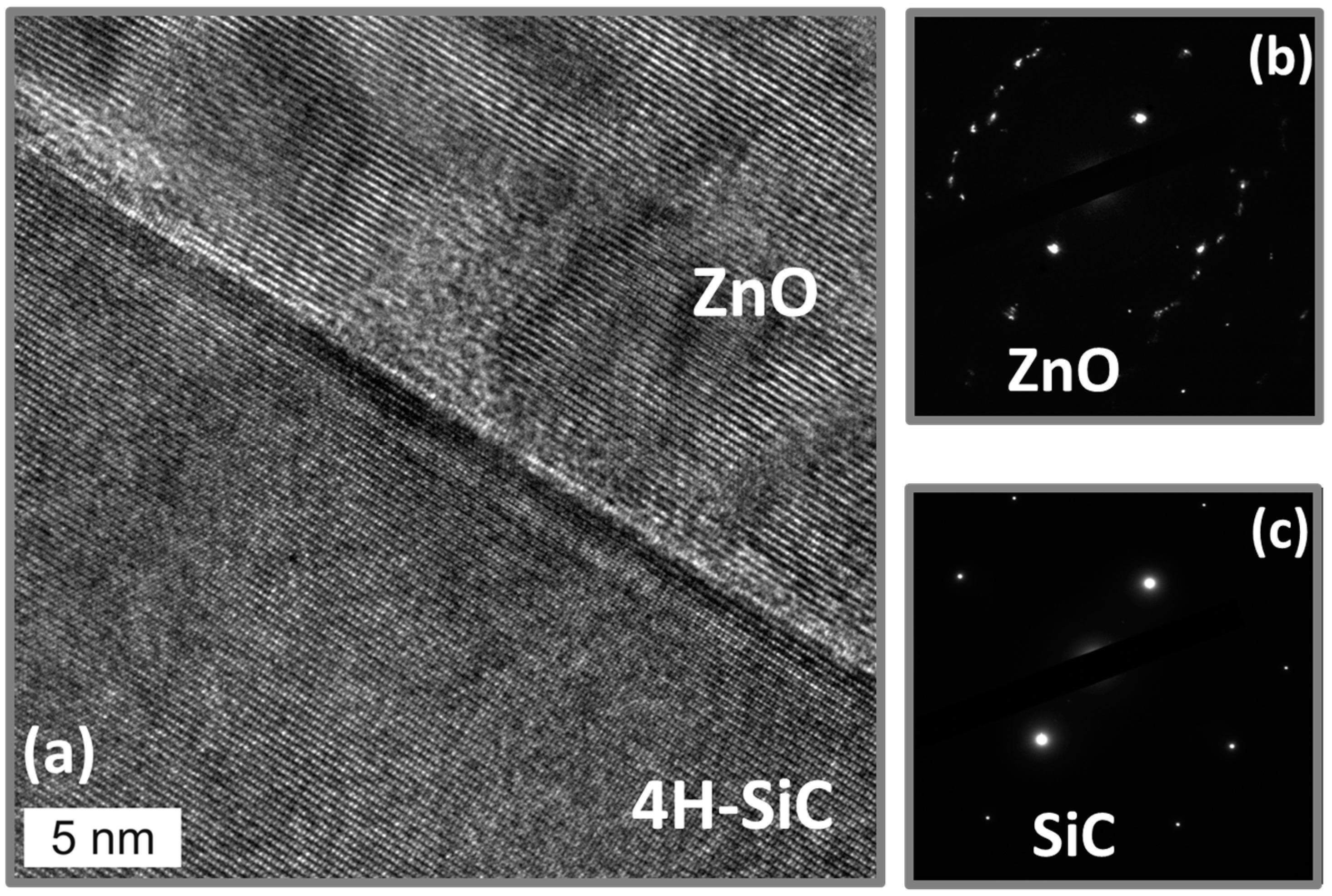
3.4. ALD Growth of ZnO onto SiC (0001-Si) Surfaces
ALD growth on SiC leads to ZnO layers with coherent atomic ordering close to the hetero-interface as evidenced in the high-resolution TEM image presented in
Figure 6a. A very thin interface, extending over very few atomic layers, is observed between ZnO and SiC, a sign of a lower interface quality as compared to the ZnO/GaN junction, for which a sharp interface is visible.
Furthermore, electron diffraction patterns, shown in
Figure 6b,c, suggest the presence of significant disordering on a larger scale, possibly related to the enhanced mosaicity.
4. Discussion
Our results from experiments of ALD growth of ZnO onto an amorphous silicon oxide surface reproduce those obtained previously by several teams [
9,
10]. The layer structure is columnar, with strong texturation of the
c-planes inside the columns parallel to the substrate surface, and strong in-plane mosaicity.
Despite the similar topology of GaAs and InP (111) surfaces and the (0001) surfaces of ZnO, it is likely that the very strong extensive lattice mismatch (>20%) between ZnO and GaAs or InP (reported in
Table 1) does not allow the induction of any significant atomic ordering between the seeding surface and the grown layer. The morphology of the layers appears to be polycrystalline, as it is for ZnO grown on an amorphous substrate surface, despite extensive studies dedicated to the cleaning and preparation of the surface of GaAs and InP before the ALD growth sequence.
On the contrary, on the GaN (0001-Ga) seeding surface, the ALD growth proceeds as a smooth pseudomorphic epitaxial process at the macroscopic scale, with coherent single-crystal stacking of ZnO onto the GaN seed and a sharp hetero-interface. This epitaxial stacking confirms and extends the results previously reported in the literature [
11,
12,
13,
14,
15] on the ALD epitaxial growth of ZnO on GaN. However, it can be noted that the epitaxial relationship is obtained with a deposition at 180 °C which is lower than the temperature used in previous works [
11,
12].
This epitaxial stacking and atomic ordering of the ZnO along the crystal structure of the seeding layer can be attributed to the similar crystal structure, together with the limited and compressive lattice mismatch factor, between ZnO and GaN.
Finally, on the 4H-SiC (0001-Si) surface, despite a much higher lattice mismatch (>5%) than ZnO/GaN (
Table 1), a remarkable atomic ordering can be obtained close to the hetero-interface, although electron diffraction shows evidence of disordering at a longer range, possibly related to the mosaicity within the ZnO layer. The hetero-interface seems somewhat less sharp than for ZnO/GaN, extending over a few atomic layers. This result is, however, encouraging and can possibly be further optimized in the future.
5. Conclusions
This paper presents preliminary results for the fabrication of electronic devices based on a ZnO heterojunction. In particular, the influence of the substrate surface structure on the morphology and crystallinity of the ALD-grown layer was studied. In addition, the deposition temperature was the main parameter that was varied in order to favor the epitaxial relationship, even though it should be mentioned that purge and pulse lengths also influence the final crystalline structure. Amorphous as well as largely mismatched starting surfaces lead to the growth of a polycrystalline (0001)-oriented ZnO layer. On the other hand, the ZnO/GaN hetero-interface appears sharp and structurally ordered, with no evidence of systematic generation of new defects at the atomic scale. The ZnO/4H-SiC hetero-interface, even if it appears less perfectly ordered, exhibits local atomic ordering. The next logical step will be to evaluate the functional properties of these hetero-interfaces by characterizing the electrical properties of test heterojunction devices.
Part of this work has been presented at the International Conference on Atomically Controlled Surfaces, Interfaces and Nanostructures (ACSIN2016) held in Frascati, Rome, Italy, on 9–15 October 2016.
Acknowledgments
This work has been supported by the French Space Agency (CNES) through a Research and Technology (R&T) project and by the European Space Agency (ESA) through a Ph.D. Grant project. It is also supported by French Defense Agency (DGA) through the DGA/ANR ASTRID project “CATHEON”. The authors acknowledge the 3-5 lab for supplying MOCVD GaN samples and Benoît Saint-Girons at INL for X-ray diffraction studies including pole figures.
Author Contributions
In this work, Jonathan Faugier-Tovar performed part of the ALD growth runs and part of the routine characterization on the ZnO layers; Florica Lazar optimized the cleaning process for GaAs and InP surfaces and characterized the ZnO layers grown on these substrates; Catherine Marichy supervised the ALD growth program; Sébastien Linas prepared the cross-section and performed the TEM studies; Christian Brylinski contributed to the implementation, organization and funding of the ALD activities at LMI lab, and he also wrote this paper. All authors have read and approved the final manuscript.
Conflicts of Interest
The authors declare no conflict of interest.
References
- Katoda, T.; Kishi, M. Heteroepitaxial growth of gallium phosphide on silicon. J. Electron. Mater. 1980, 4, 783–796. [Google Scholar] [CrossRef]
- Mitin, V.F.; Lazrarov, V.K.; Lari, L.; Lytvyn, P.M.; Kholevchuk, V.V.; Matveeva, L.A.; Mitin, V.V.; Venger, E.F. Effect of film growth rate and thickness on properties of Ge/GaAs(100) thin films. Thin Solid Films 2014, 550, 715–722. [Google Scholar] [CrossRef]
- Bratina, G.; Nicolini, R.; Sorba, L.; Vanzetti, L.; Mula, G.; Yu, X.; Franciosi, A. ZnSe-GaAs heterojunction parameters. J. Cryst. Growth 1993, 127, 387–391. [Google Scholar] [CrossRef]
- Liu, L.; Edgar, J.H. Substrates for gallium nitride epitaxy. Mater. Sci. Eng. R Rep. 2002, 37, 61–127. [Google Scholar] [CrossRef]
- Miikkulainen, V.; Leskelä, M.; Ritala, M.; Puurunen, R.L. Crystallinity of inorganic films grown by atomic layer deposition: Overview and general trends. J. Appl. Phys. 2013, 113, 021301. [Google Scholar] [CrossRef]
- Tsukazaki, A.; Akasaka, S.; Nakahara, K.; Ohno, Y.; Ohno, H.; Maryenko, D.; Ohtomo, A.; Kawasaki, M. Observation of the fractional quantum Hall effect in an oxide. Nat. Mater. 2010, 9, 889–893. [Google Scholar] [CrossRef] [PubMed]
- Sbrockey, N.M.; Ganesan, S. ZnO thin films by MOCVD. 2004, 17, 23–25. [Google Scholar] [CrossRef]
- Tynell, T.; Karppinen, M. Atomic layer deposition of ZnO: A review. Semicond. Sci. Technol. 2014, 29, 043001. [Google Scholar] [CrossRef]
- Chai, Z.; Lu, X.; He, D. Atomic layer deposition of zinc oxide films: Effects of nanocrystalline characteristics on tribological performance. Surf. Coat. Technol. 2012, 207, 361–366. [Google Scholar] [CrossRef]
- Tapily, K.; Gu, D.; Baumgart, H.; Namkoong, G.; Stegall, D.; Elmustafa, A. Mechanical and structural characterization of atomic layer deposition-based ZnO film. Semicond. Sci. Technol. 2011, 26, 115005. [Google Scholar] [CrossRef]
- Särkijärvi, S.; Sintonen, S.; Tuomisto, F.; Bosund, M.; Suihkonen, S.; Lipsanen, H. Effect of growth temperature on the epitaxial growth of ZnO on GaN by ALD. J. Cryst. Growth 2014, 398, 18–22. [Google Scholar] [CrossRef]
- Baji, Z.; Lábadi, Z.; Molnár, G.; Pécz, B.; Vad, K.; Horváth, Z.E.; Szabó, P.J.; Nagata, T.; Volk, J. Highly conductive epitaxial ZnO layers deposited by atomiclayer deposition. Thin Solid Films 2014, 562, 485–489. [Google Scholar] [CrossRef] [Green Version]
- Chiang, T.-Y.; Dai, C.-L.; Lian, D.-M. Influence of growth temperature on the optical and structural properties of ultrathin ZnO films. J. Alloy. Compd. 2011, 509, 5623–5626. [Google Scholar] [CrossRef]
- Min, Y.-S.; An, C.J.; Kim, S.K.; Song, J.; Hwang, C.S. Growth and Characterization of Conducting ZnO Thin Films by Atomic Layer Deposition. Bull. Korean Chem. Soc. 2010, 31, 2503–2508. [Google Scholar] [CrossRef]
- Lin, C.-W.; Ke, D.-J.; Chao, Y.-C.; Chang, L.; Liang, M.-H.; Ho, Y.-T. Atomic layer deposition of epitaxial ZnO on GaN and YSZ. J. Cryst. Growth 2007, 298, 472–476. [Google Scholar] [CrossRef]
© 2017 by the authors; licensee MDPI, Basel, Switzerland. This article is an open access article distributed under the terms and conditions of the Creative Commons Attribution (CC-BY) license ( http://creativecommons.org/licenses/by/4.0/).


