The Electrical and Structural Properties of Nitrogen Ge1Sb2Te4 Thin Film

Department of Physics, Faculty of Sciences, University of Craiova, A.I. Cuza No. 1, Craiova 200585, Romania
Coatings 2018, 8(4), 117; https://doi.org/10.3390/coatings8040117
Submission received: 24 January 2018
/
Revised: 20 March 2018
/
Accepted: 21 March 2018
/
Published: 23 March 2018
Abstract
:The present work describes the process of obtaining thin films of Ge1Sb2Te4 by means of the short-pulse High Power Impulse Magnetron Sputtering (HiPIMS) technique. The Ge1Sb2Te4 (GST-124) and nitrogen Ge1Sb2Te4 (nitrogen GST-124) films were obtained in HiPIMS plasma ignited in Ar/GST-124 and Ar/N2/GST-124, respectively. In particular, the possibility of tailoring the electrical properties of films for applications in the phase change memory (PCM) cells was investigated. The I–V measurements performed in a voltage sweeping mode on GST-124 and nitrogen GST-124 show that the threshold switching voltage varies as a function of nitrogen level in HiPIMS plasma. Amorphous-to-crystalline trigonal phase transition of the films was induced by thermal annealing, and structural changes were identified using X-ray diffraction and Raman scattering spectroscopy. The most intense bands appeared for the annealed layers in the range of 138–165 cm−1, for GST-124, and 138–150 cm−1 for nitrogen GST-124, respectively.
1. Introduction
Over the last few years, phase change memory (PCM) based on the GeSbTe (GST) chalcogenide has attracted attention in the field of microelectronics technology. Advantages, such as its high speed, high density, and low power consumption [1,2] suggest that it will play a prominent role among the next generation of materials which will supersede existing, nonvolatile memories.
The principle of a phase change memory has been demonstrated since the 1960s [3] for nonvolatile electronic memories. For phase change memories, switching is performed by means of Joule heating that can effectively switch the material between amorphous and crystalline phases, which have very different optical and electrical properties [4].
The characteristics of PCM change significantly when the atomic structure of material is transformed by applying heat, electrical and optical pulses. The energy required to switch between the two phases (amorphous to crystalline) depends on the material properties, and also on the structural design of the device fabrication. Among these systems, interfacial phase change memory (iPCM) materials composed of GeTe and Sb2Te3 super-lattices (SLs) have attracted technological and scientific interest due to their improved switching characteristics, including lower energy consumption. The hexagonal Sb2Te3 and cubic GeTe layer in super-lattice structure generates a material allowing Ge atoms switch between octahedral sites and lower-coordination sites at the interface of the super-lattice layers. It has been shown that the GeTe/Sb2Te3 interfacial phase-change memories data storage device with reduced switching energy could improve both the write/erase cycle lifetime and the speed of switching [5,6].
The local atomic arrangements of layered Ge–Sb–Te compounds are fundamentally important for data storage applications. Recently, the local atomic arrangements and the lattice distortion in the Ge–Sb–Te thin film were studied by using a combination of atomic-resolution aberration-corrected (Cs-corrected) high-angle annular dark-filed scanning transmission electron microscopy (HAADF-STEM). The reported results showed that thin films are formed by the stacking of individual building blocks of GST-225, with GST-124 crystal structures intercalated inside randomly oriented grains [7]. The fast change from the amorphous to the metastable phase of GST films done by laser irradiation was studied by aberration-corrected scanning transmission electron microscopy (Cs-corrected STEM). The rapid transition between the amorphous and metastable GST phases was explained by the similarity in the local atomic arrangements between these phases and by small distortions of the GST lattice [8].
Therefore, GeSbTe became a possible candidate as an active material for phase change random access memory (PRAM) devices due to its rapid switching speed and is well modified for use in semiconductors fabrications. However, large reset current and short device retention time associated with GeSbTe are significant problems. To overcome these, doping with various elements changes the properties of the materials based on chalcogenide, and improves the device’s characteristics. A large variety of dopants have been considered, including N [9,10,11], O [10,12,13], Si [14,15], Sn [16,17], Ta2O5 [18], Ag [19], but a complete understanding of their effects has still not been obtained. At present, many studies have been developed to solve these issues by either experimental methods or theoretical calculations.
The addition of dopants into GST leads to larger resistance in the crystalline phase, with a beneficial reduction of write current, and a significantly improved retention time of the amorphous phase due to the increased crystallization temperature.
Nitrogen-doped Ge2Sb2Te5 has also been studied to improve the performance of PRAM. When nitrogen is introduced into a GST film, it forms nitrides, which inhibit crystalline grain growth. The inhibition of crystalline growth reduces reamorphization current and improves the endurance of PRAM devices [12,20]. The efficacy of the Ge2Sb2Te5 based PCM cell, and multiple phase-transition phenomena, were evidenced by the current–voltage (I–V) measurements during current sweeping mode [21].
Based on the data reported in ref. [20], the phase change of GST-124 doped with nitrogen (15% and 30% nitrogen in GST-124, respectively) was investigated by sheet resistance as a function of annealing temperature, where three temperatures in a range of 160–190 °C appeared. The sharp drop at about 160 °C was attributed to amorphous-to-face centered cubic (fcc) transition; the small drop at about 180–190 °C was attributed to fcc-to-trigonal transition. In addition, the drop in sheet resistance at 165 °C was explained by phase segregation, since the alloy with a lower excess of Te shows two transitions at low annealing temperature (caused by Te crystallite segregation). Moreover, a significant dependence on nitrogen content in GST-124 was not observed.
This study is focused on the phase change phenomena which occurs in current-voltage measurements for the GST-124 and nitrogen GST-124, respectively. The phase change from amorphous to fcc, and further to trigonal crystalline states, was observed. The electrodes were deposited onto the substrate by thermionic vacuum arc [22,23]. The GST-124 and nitrogen Ge1Sb2Te4 thin films were deposited on the silicon substrate by the reactive High Power Impulse Magnetron Sputtering (HiPIMS) technique [24]. It is well known that, due to the very high electron density in HiPIMS, both sputtered metal flux and reactive gas flux are highly ionized, leading to an increased reactivity on the film surface and a better and easier control of the elemental and phase composition of the compound films [25,26,27].
2. Experimetal
The GST-124 and nitrogen GeSbTe-124 thin films were deposited by HiPIMS with a 3” torus magnetron [24]. A 3” diameter × 0.2” thick GST-124 ceramic target (provided by Kurt J. Lesker, Jefferson Hills, PA, USA) was used and silicon pieces axially placed in the deposition system were used as substrates. The target-to-substrate distance was about 8 cm and the sputtering time was 30 min at a power of 30 W. The target peak-power of 10–15 kW was reached during the HiPIMS operation (for −950 V applied voltage, pulse width of 20 μs and pulse frequency ranged between 100 and 200 Hz).
A mixture of high purity Ar and N2 was used as sputtering gas at a constant pressure of 0.66 Pa; flow rates were Ar 6 sccm and N2 (0–10) sccm. For a low N2 flow (less than 10 sccm), the Ge1Sb2Te4 film grows in the crystalline phase due to the generation of secondary electrons in the HiPIMS plasma, which could heat the substrate.
The thickness of the deposited films, measured using a Quartz Crystal Microbalance (Inficon Q-pod, Bad Lagaz, Switzerland), was of about 200 nm. The silver electrodes were deposited by thermionic vacuum arc and had a thickness of 500 nm. In order to correlate the modifications induced by the voltage sweeping mode process on the phase changes, some of samples were annealed at different temperatures in a vacuum, with heating and cooling rates of 5 °C/min, respectively. The samples were kept for 1 min at the desired temperature. The crystalline evolution of the GST-124 layers was checked by X-ray diffraction measurements (XRD-6000, Szimadzu, Kyoto, Japan) in the thin film configuration, while the vibration modes were determined by confocal a Raman microscope Renishaw (Renishaw plc, Gloucestershire, UK), equipped with a laser at 532 nm. The surface topography of films was investigated by atomic force microscopy (AFM) Park system (NC-AFM, Park Systems, Suwon, Korea). The I–V measurements were done with 2400 Keithley source meter (Keithley, Cleveland, OH, USA).
3. Results and Discussions
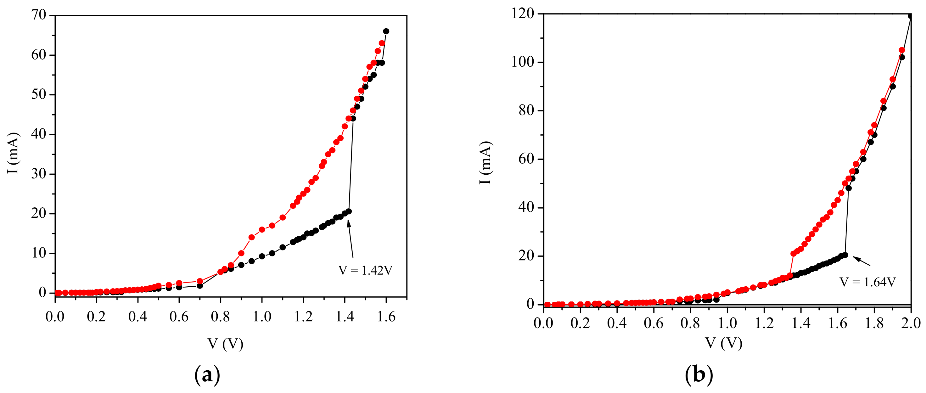
The I–V measurements of thin film were performed in the voltage sweep mode to confirm the switching properties for GST-124 and nitrogen GST-124, respectively. During the first sweep, the amorphous GST-124 layer became crystallized (the Joule effect) at a threshold switching voltage of 1.42 V; the then current abruptly increases, and as a consequence, the layer changes from insulator to semiconductor (Figure 1a).
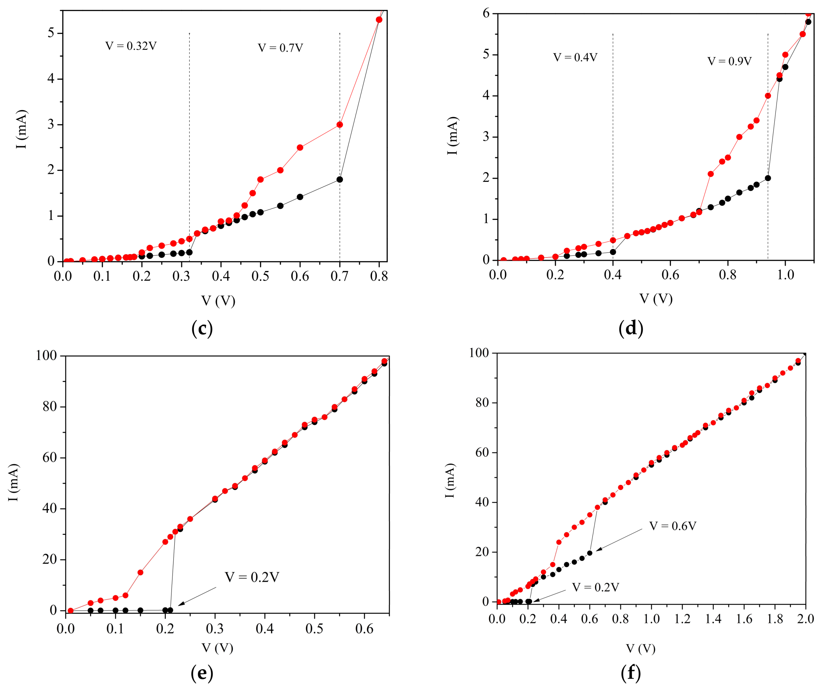
For the nitrogen GST-124, an increase of the threshold switching voltage at 1.62 V, as seen in Figure 1b, was observed. In both cases presented in Figure 1c,d, during the first voltage sweep, a low threshold voltage between 0.3 and 0.9 V was observed in the I–V measurements.
A rapid rise of the current was observed in the electrical behavior for the GST-124 thin film annealed at 400 °C, as seen in Figure 1e. During the first sweep, a low threshold voltage of 0.2 V corresponds to a mixture of fcc and trigonal phases in the layer.
For the nitrogen GST-124 sample annealed at 400 °C, in the first sweep two threshold voltage values at 0.2 and 0.6 V are observed, as seen in Figure 1f. The first threshold voltage (0.2 V) is associated with the change between the amorphous-to-fcc phases. The second threshold voltage (0.6 V) is related to the mixing of fcc and trigonal phases. These low threshold values in the first sweep for annealed and non-annealed samples are related to the various resistances of the GST-124 layers.
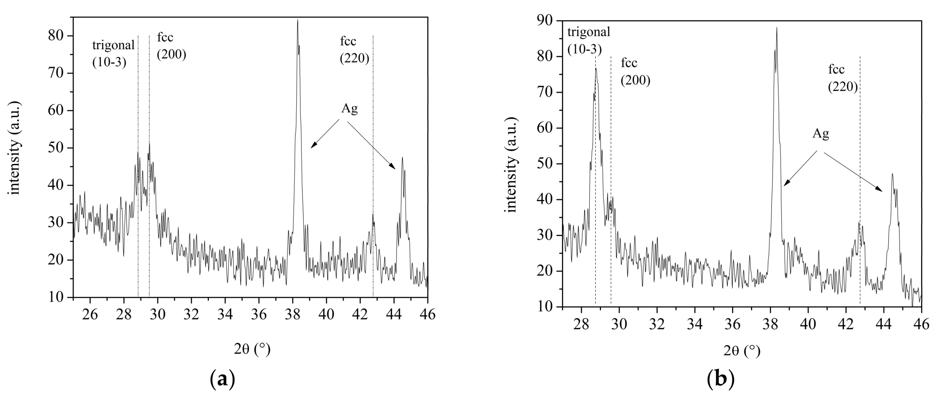
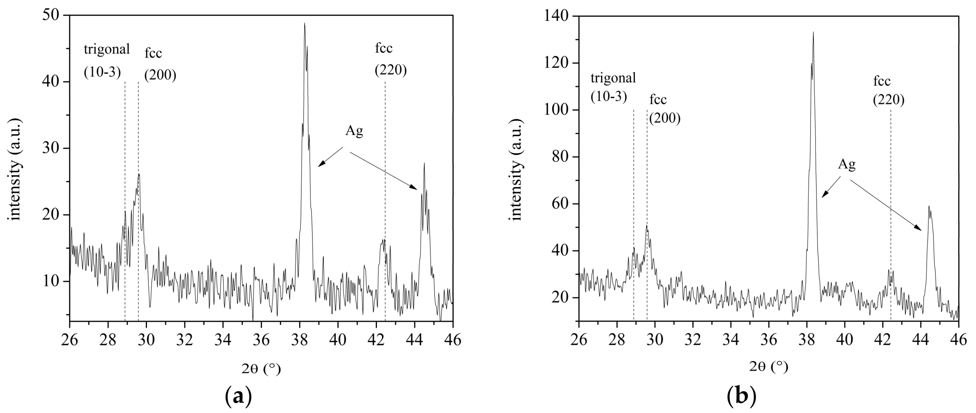
To understand the effect of the switching thresholds observed in the I–V measurements for the GST-124 and nitrogen GST-124 films, XRD measurements were performed at various annealing temperatures from 150 to 400 °C. The XRD studies show that the GST-124 has three phases at different temperatures, as seen in Figure 2a–c.
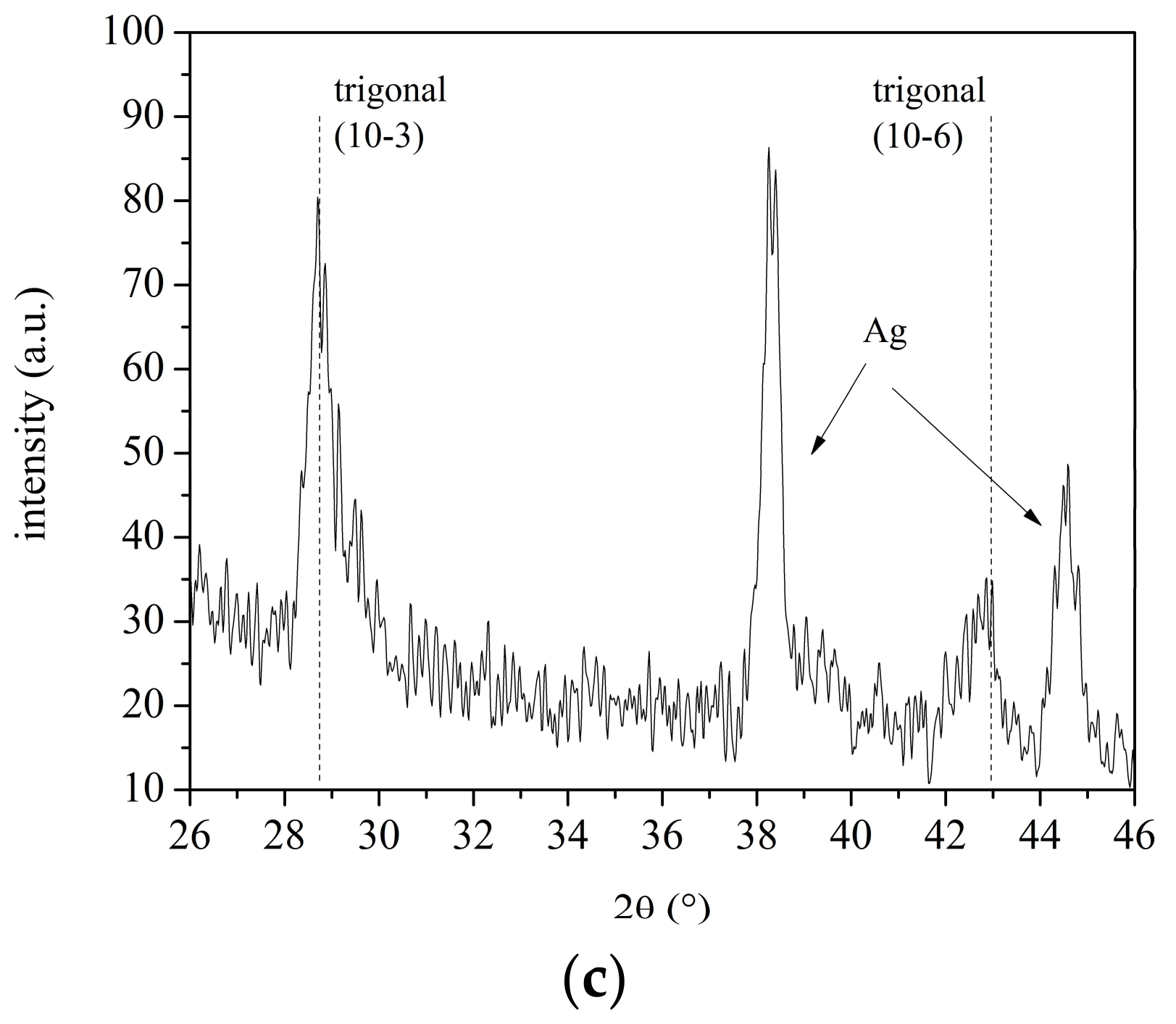
In the 100–150 °C temperature range, the GST-124 film is in the amorphous phase. Following an increase in the annealing temperature from 150 to 275 °C, the film presented the fcc crystalline phase. At an annealing temperature of 275 °C, a peak appears at 28.9°, indicating the formation of a trigonal phase in the fcc crystalline matrix. A temperature of 275 °C is the limit of the fcc and trigonal phases. In the annealing temperature range of 275–400 °C, the mixing of fcc and trigonal crystalline phases in the film is observed.
The XRD measurements show an amorphous phase for the nitrogen GST-124 thin film up to a temperature of 165 °C. Increasing the temperature up to 375 °C, the presence of fcc crystalline phase is observed, while a mixture of fcc and trigonal phases corresponds to 440 °C (Figure 3a,b). A clear trigonal crystalline phase is not reached. When the HiPIMS plasma is ignited in Ar/N2/GST-124 and nitrogen is incorporated into a GST film, the crystalline phase is suppressed, resulting in an increase in the crystallization temperature.
Correlating the I–V measurements with XRD studies, the thresholds in the first voltage sweep of the sample could be associated with the crystallization of GST-124 (the Joule effect, due to the voltage sweep).
The voltage step value of 1.42 V observed in Figure 1a, where the heat of the film produced by Joule effect is sufficient, corresponds to trigonal phase. In Figure 1c, the first voltage step at 0.3 V corresponds to crystallization of amorphous film by voltage sweeping. The second voltage step at 0.7 V corresponds to the existence fcc-trigonal mixing phases.
For the sample annealed at a temperature of 400 °C presented in Figure 1e, the step value with 0.2 V threshold in the first voltage sweep might be connected with the fcc and trigonal phase mixing.
A similar behavior is observed for the nitrogen GST-124 films. In Figure 1d, two step voltage threshold values at 0.4 and 0.9 V are presented. The first step corresponds to the crystallization of amorphous film due to voltage sweeping while the second step is related to mixing of fcc and trigonal phases.
For the annealed nitrogen GST-124 film, two steps of voltage sweep at threshold values of 0.2 and 0.6 V were observed in Figure 1f. The first threshold voltage (0.2 V) is connected with the fcc phase, while the second (0.6 V) corresponds to fcc and trigonal mixing phases. In the case of nitrogen GST-124 sample, the transition temperatures of various phases reached higher values than with the GST-124 film, since the nitrogen content suppressed the crystalline phase formation.
It is obvious that the crystallization temperature increases with nitrogen content in the film, indicating a better thermal stability of the crystalline phase, which could result in improving data retention of the PCM cells.
Since the switching process from fcc-to-trigonal phase for nitrogen film requires a higher temperature, this process shows promise for phase change memories technology.
In reference [28] it was established that the resistivity of GST-225 and GST-147 compounds, respectively, decreased with the application of various peak current density values. It was demonstrated in reference [28] that the transition from insulator to metal is done without phase transition by using an electric peak current (an outcome which differs from that of thermal annealing). In this case, it provided a pathway for promoting vacancy rearrangements using an electric current; the role of the electrical current is a kinetic factor which accelerates the rearrangement process. The applied current can migrate atoms by momentum transfer from the charge carriers, known as electromigration. Phase transitions require more energy to generate a new phase compared with vacancy rearrangements because the phase transitions are accompanied by changes in atoms.
Relating to these results, in our experiments the explanation of vacancies formation in the I–V measurements of GST-124 film might be convincing. However, in nitrogen GST-124 film could not be supported due to nitrides formation. In the present I–V measurements, done in a voltage sweeping mode, the electrical current measured is not high (microamps range). This implies that the atomic displacement by a low current is negligible compared to that of a high current, because the driving force is insufficient to generate a massive flux of atoms. Therefore, in the measurements of the present study, the existence of phase mixing was assumed.
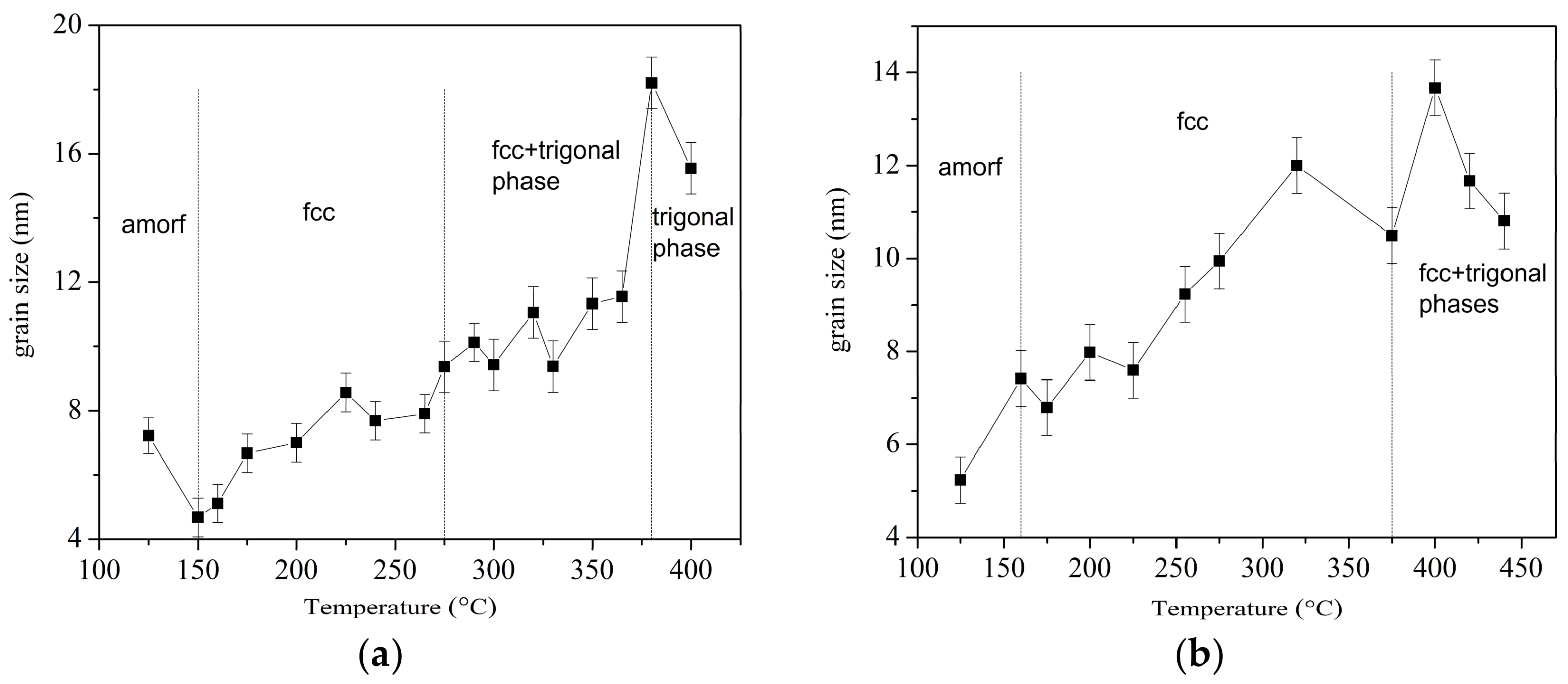
In addition, looking at the grain size presented in Figure 4a,b of the nitrogen GST-124, unlike in the GST-124 film, the fcc phase is preserved at higher temperature range for the nitrogen incorporated in films. The evaluation of the grain size of the crystallized films was done using the (200) and (10-3) diffraction peaks, according to the Scherrer formula. Grain sizes increase with the rise of the annealing temperature.
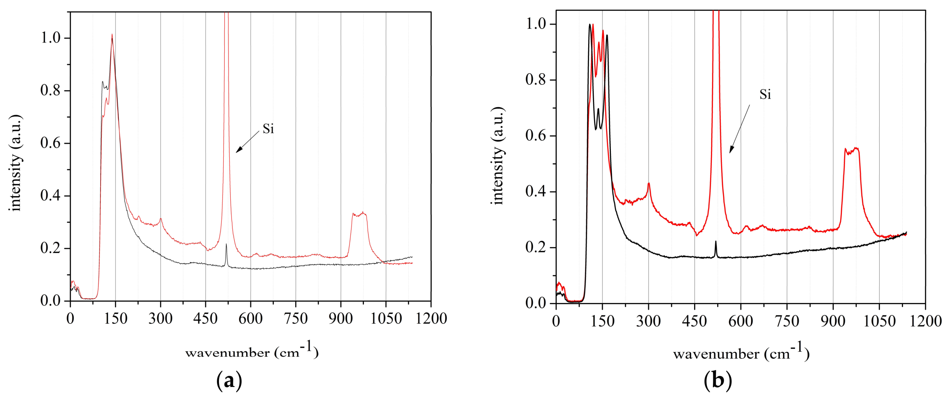
Raman measurements were carried out in order to reveal the chemical bonding in GST-124 and nitrogen GST-124 films, respectively. The Raman data recorded on as-deposited GST-124 and nitrogen GST-124 films were dominated by two vibration modes, at 110 cm−1 and a broad band in the range of 127–160 cm−1 having a peak of 138 cm−1, respectively. The band peak at 110 cm−1 is assigned to the GeTe, Г1(A1) mode, and the broad peak to Sb2Te3 to Eg(2) and A1g(2) modes, respectively [29]. Increasing the temperature to 400 °C, the spectra displayed several changes: in the GST-124, the peak at 107 cm−1 is increasing, which is associated with the GeTe, Г1(A1) mode, and the broad band peak is splitting into two peaks at 138 cm−1 and 165 cm−1, respectively.
The peak of 138 cm−1 is assigned to Ge–Te bonds [2]. The A1g(2) Raman-active mode of crystalline GST-124 presented at 165–168 cm−1 is assigned to the Sb2Te3 vibration [29,30].
For nitrogen GST-124 layers, the Raman data are dominated by three peaks: a small peak at 107 cm−1, one at 120 cm−1 and the broadband at 126–160 cm−1 with a peak at 138 cm−1. The doped sample is dominated by the Sb–Te vibration due to the higher polarizability leading to strong mask effect [29]. An increase in the annealing temperature changed the Raman spectra considerably. The peak at 107 cm−1, related to Ge–Te vibration bands strongly decreased, whereas an increase in intensity of the peak at 120 cm−1 was observed. The Raman band with maxima at ~120–125 cm−1 can be attributed to the vibrations of GeTe4−nGen (n = 1, 2) corner-sharing tetrahedra (A1 mode) according to the assignment in the amorphous GeTe layers.
The broad peak is splitting into two peaks at 138 cm−1 and 150 cm−1, respectively. The peak of 138 cm−1 is assigned to Ge–Te bonds [2], whereas several alternative interpretations are possible for the peak at 150 cm−1. Some authors believe that this peak is associated with Te–Te stretching mode [31,32]. Others researchers associated this peak to vibrations of Sb–Te stretching bonds in SbTe3/2 structural units [33]. Under the present study, this interpretation is most convincing, since at higher annealing temperature Te–Te stretching bonds are unlikely to appear. In Figure 5a,b, the broad peaks of the nitrogen GST-124 film presented at high wavenumber values, 900–1000 cm−1, could be attributed to nitrides formation during doping.
In the case of nitrogen GST-124, a peak at 300 cm−1 is associated with the Ge–Ge stretching vibrations. Its position does not change with temperature. The position of this peak can change depending on various factors, such as cluster size, stress, composition. A very weak Raman band with a peak at 220 cm−1 is related to GeTe4−nGen tetrahedra vibrations antisymmetric stretching modes [34].
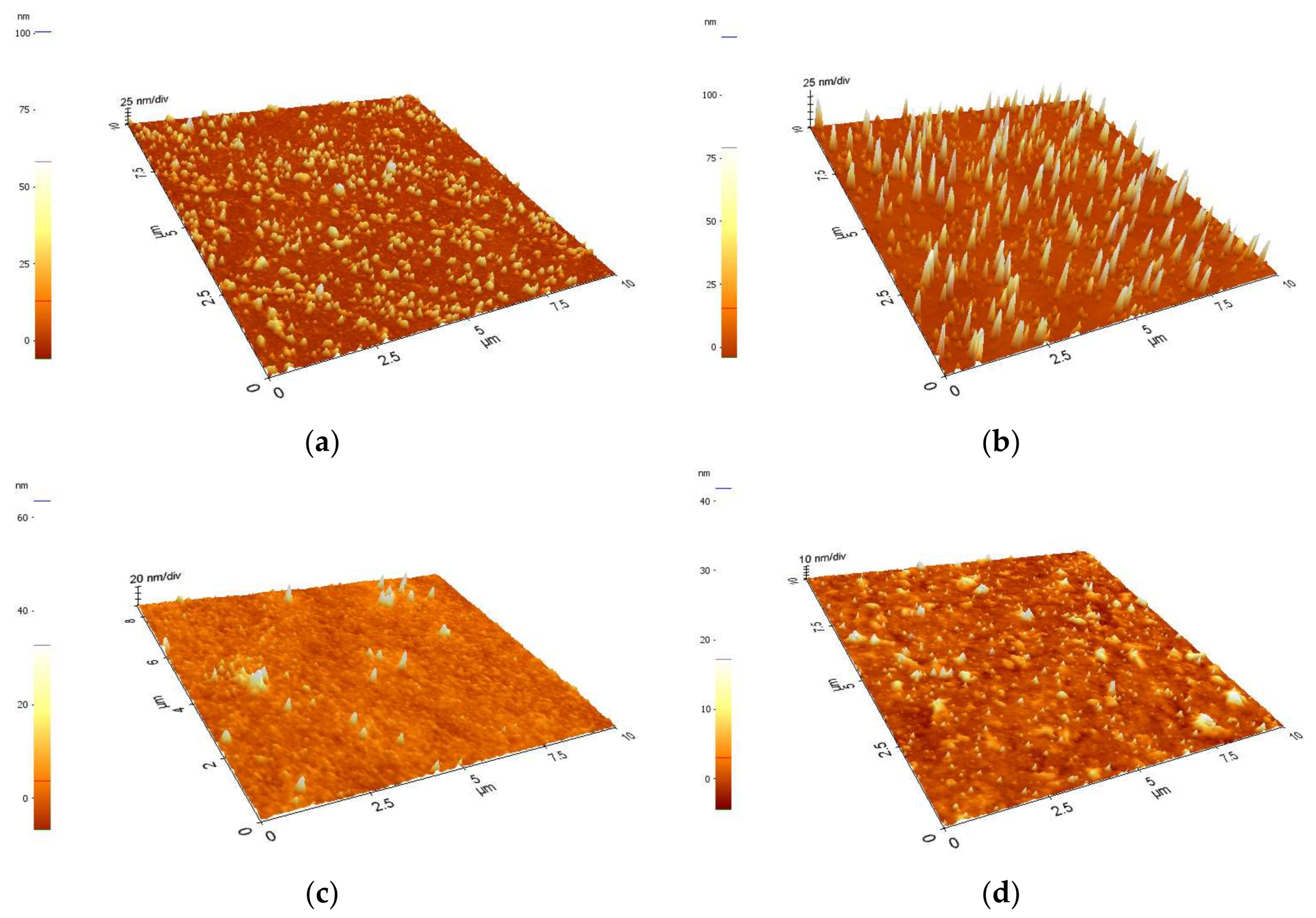
Atomic force microscopy images presented in Figure 6 show the difference in the crystalline growth modes due to the formation of different phases in GST-124 and nitrogen GST-124 film, respectively. At room temperature, the sample’s surfaces seem to be rather similar (the difference being mostly in terms of roughness, which is 5.839 nm for GST-124 and 5.419 nm for nitrogen GST-124, respectively). After an annealing treatment at 400 °C, the GST-124 film contains grains dominated by the trigonal phase while the nitrogen film contains grains having mixed phases. At this temperature, the roughness levels of GST-124 and nitrogen GST-124 films are 2.063 nm and 1.796 nm, respectively.
4. Conclusions
To conclude, the authors have demonstrated the dependence of structural, morphological, and electrical properties of GST-124 thin films on the nitrogen content and the annealing temperature. For the I–V characteristics measured for GST-124 and nitrogen GST-124, it was observed that the voltage switching threshold values varied with the nitrogen content. The I–V measurements show switching thresholds at low voltage values that were associated with the phase change during sweeping voltage due to the Joule heat and the annealing treatment. The X-ray measurements confirmed the existence of a phase change film during the I–V measurements in voltage sweeping. Unlike the GST-124, the fcc structure for the nitrogen GST-124 was preserved in a large annealing temperature range. The Raman measurements illustrate the most intensive mode during annealing treatment. It was observed that the 138 cm−1 vibration mode is common to both films. The modes at higher wavenumber values at 900–1000 cm−1 could be related to the formation of nitrides during nitrogen doping. AFM measurements confirm a very small roughness on the films’ surfaces; at higher annealing temperatures the GST-124 film contains grains dominated by the trigonal phase.
Acknowledgments
The financial support of this work done in the frame of The Partnership National Research Project number 174/2012-2017 PCCA type 2. There are not funds for covering the costs to publish in open access.
Conflicts of Interest
The author declares no conflict of interest.
References
- Wuttig, M.; Yamada, N. Phase-change materials for rewriteable data. Nat. Mater. 2007, 6, 824–832. [Google Scholar] [CrossRef] [PubMed]
- Peng, C.; Wu, L.; Rao, F.; Song, Z.; Zhou, X.; Zhu, M.; Liu, B.; Yao, D.; Feng, S.; Yang, P.; et al. Nitrogen incorporated GeTe phase change thin film for high-temperature data retention and low-power application. Scr. Mater. 2011, 65, 327–330. [Google Scholar] [CrossRef]
- Ovshinsky, S. Reversible electrical switching phenomena in disordered structures. Phys. Rev. Lett. 1968, 21, 1450–1453. [Google Scholar] [CrossRef]
- Lankhorst, M.H.R.; Ketelaars, B.W.S.M.M.; Wolters, R.A.M. Low cost and nanoscale non-volatile memory concept for future silicon chip. Nat. Mater. 2005, 4, 347–352. [Google Scholar] [CrossRef] [PubMed]
- Simpson, R.E.; Fons, P.; Kolobov, A.V.; Fukaya, T.; Krbal, M.; Yagi, T.; Tominaga, J. Interfacial phase-change memory. Nat. Nanotechnol. 2011, 6, 501–505. [Google Scholar] [CrossRef] [PubMed]
- Lotnyk, A.; Hilmi, I.; Ross, U.; Rauschenbach, B. Van der Waals interfacial bonding and intermixing in GeTe Sb2Te3 based supperlatices. Nano Res. 2018, 11, 1676–1686. [Google Scholar] [CrossRef]
- Lotnyk, A.; Ross, U.; Bernutz, S.; Thelander, E.; Rauschenbach, B. Local atomic arrangements and lattice distortions in layered Ge-Sb-Te crystal structures. Sci. Rep. 2016, 6, 26724. [Google Scholar] [CrossRef] [PubMed]
- Lotnyk, A.; Bernütz, S.; Sun, X.; Ross, U.; Ehrhardt, M.; Rauschenbach, B. Real-space imaging of atomic arrangement and vacancy layers ordering in laser crystallized Ge2Sb2Te4 phase change thin films. Acta Mater. 2016, 105, 1–8. [Google Scholar] [CrossRef]
- Borisenko, K.B.; Chen, Y.X.; Song, S.A.; Cockayne, D.J.H. Nanoscale phase separation and building blocks of Ge2Sb2Te5N and Ge2Sb2Te5N2 thin films. Chem. Mater. 2009, 21, 5244–5251. [Google Scholar] [CrossRef]
- Privitera, S.; Rimini, E.; Zonca, R. Amorphous to crystal transition of nitrogen and oxygen doped Ge2Sb2Te4 films studied by in situ resistance measurements. Appl. Phys. Lett. 2004, 85, 3044–3046. [Google Scholar] [CrossRef]
- Kim, Y.K.; Jeong, K.; Cho, M.H.; Hwang, U.; Jeong, H.S.; Kim, K. Changes in the electronic structures and optical band gap of Ge2Sb2Te5and N-doped Ge2Sb2Te5 during phase transition. Appl. Phys. Lett. 2007, 90, 171920. [Google Scholar] [CrossRef]
- Song, K.B.; Sohn, S.W.; Kim, J.; Kim, K.A.; Cho, K. Chalcogenide thin-film transistors using oxygenated n-type and p-type phase change materials. Appl. Phys. Lett. 2008, 93, 043514. [Google Scholar] [CrossRef]
- Jang, H.; Park, S.J.; Lim, D.H.; Cho, M.H.; Do, K.H.; Ko, D.H.; Sohn, H.C. Phase change behavior in oxygen-incorporated Ge2Sb2Te5 films. Appl. Phys. Lett. 2009, 95, 012102. [Google Scholar] [CrossRef]
- Cho, E.; Han, S.; Kim, D.; Horii, H.; Nam, H.S. Ab initio study on influence of dopants on crystalline and amorphous Ge2Sb2Te5. J. Appl. Phys. 2011, 109, 043705. [Google Scholar] [CrossRef]
- Feng, J.; Zhang, Y.; Qiao, B.W.; Lai, Y.F.; Lin, Y.Y.; Cai, B.C.; Tang, T.A.; Chen, B. Si doping in Ge2Sb2Te5 film to reduce the writing current of phase change memory. Appl. Phys. A 2007, 87, 57–62. [Google Scholar] [CrossRef]
- Zhou, J.; Sun, Z.M.; Xu, L.H.; Ahuja, R. Effect of dopants on the structure and properties of Ge2Sb2Te5 studied by Ab initio calculations. Solid State Commun. 2008, 148, 113–116. [Google Scholar] [CrossRef]
- Song, W.D.; Shi, L.P.; Miao, X.S.; Chong, T.C. Phase change behaviors of Sn-doped Ge–Sb–Te material. Appl. Phys. Lett. 2007, 90, 091904. [Google Scholar] [CrossRef]
- Song, S.; Song, Z.; Wu, L.; Liu, B.; Feng, S. Stress reduction and performance improvement of phase change memory cell by using Ge2Sb2Te5–TaOx composite films. J. Appl. Phys. 2011, 109, 034503. [Google Scholar] [CrossRef]
- Song, K.H.; Kim, S.W.; Seo, J.H.; Lee, H.Y. Characteristics of amorphous Ag0.1Ge2Sb2Te5 thin film and its ultrafast crystallization. J. Appl. Phys. 2008, 104, 103516. [Google Scholar] [CrossRef]
- Osiac, M.; Tiron, V.; Iacobescu, G.E. The effect of nitrogen doping on the structure of Ge1Sb2Te4. J. Optoelectron. Adv. Mater. 2015, 17, 1471–1475. [Google Scholar]
- Wu, L.; Song, Z.; Liu, B.; Zhang, T.; Rao, F.; Shen, J.; Wang, F.; Feng, S. Multiple phase-transition in Ge2Sb2Te5 based phase change memory cell by current-voltage measurement. J. Non-Cryst. Solids. 2007, 353, 4043–4047. [Google Scholar] [CrossRef]
- Jepu, I.; Porosnicu, C.; Mustata, I.; Lungu, C.P.; Kuncser, V.; Osiac, M.; Iacobescu, G.; Ionescu, V.; Tudor, T. Simultaneously thermionic vacuum arc discharges in obtaining ferromagnetic thin films. Rom. Rep. Phys. 2011, 63, 804–816. [Google Scholar]
- Ionescu, V.; Osiac, M.; Lungu, C.P.; Pompilian, O.G.; Jepu, I.; Mustata, I.; Iacobescu, G.E. Morphological and structural investigation of the Co-MgF2 granular thin films by thermionic vacuum arc. Thin Solid Films 2010, 518, 3945–3948. [Google Scholar] [CrossRef]
- Osiac, M.; Tiron, V.; Iacobescu, G.E.; Popa, G. A comparative study of GeSb2Te4 films deposited by radiofrequency and pulsed direct-current and magnetron sputtering high power impulse magnetron sputtering. Dig. J. Nanomater. Biostruct. 2014, 9, 451–457. [Google Scholar]
- Tiron, V.; Sirghi, L.; Popa, G. Control of aluminum doping of ZnO: Al thin films obtained by high-power impulse magnetron sputtering. Thin Solid Films 2012, 520, 4305–4309. [Google Scholar] [CrossRef]
- Tiron, V.; Velicu, I.L.; Stanescu, D.; Magnan, H.; Sirghi, L. High visible light photocatalytic activity of nitrogen-doped ZnO thin films deposited by HiPIMS. Surf. Coat. Technol. 2016, 324, 594–600. [Google Scholar] [CrossRef]
- Tiron, V.; Velicu, I.L.; Dobromir, M.; Demeter, A.; Samoila, F.; Ursu, C.; Sirghi, L. Reactive multi-pulse HiPIMS deposition of oxygen-deficient TiOx thin films. Thin Solid Films 2016, 603, 255–261. [Google Scholar] [CrossRef]
- Park, Y.-J.; Cho, J.-Y.; Jeong, M.-W.; Na, S.; Joo, Y.-C. New pathway for the formation of metallic cubic phase Ge–Sb–Te compounds induced by an electric current. Sci. Rep. 2016, 6, 21466. [Google Scholar] [CrossRef] [PubMed]
- Němec, P.; Nazabal, V.; Moreac, A.; Gutwirth, J.; Beneš, L.; Frumar, M. Amorphous and crystallized Ge–Sb–Te thin films deposited by pulsed laser: Local structure using Raman scattering spectroscopy. Mater. Chem. Phys. 2012, 136, 935–941. [Google Scholar] [CrossRef]
- Jigau, M.; Osiac, M.; Iacobescu, G.E. Influence of the annealing temperature on the Ge1Sb2Te4 thin film prepared by pulsed laser deposition. J. Optoelectron. Adv. Mater. 2017, 19, 395–399. [Google Scholar]
- Liu, B.; Song, Z.T.; Zhang, T.; Feng, S.L.; Chen, B. Raman spectra and XPS studies of phase changes in Ge2Sb2Te5 films. Chin. Phys. 2004, 13, 1947. [Google Scholar]
- Tominaga, J.; Atoda, N. Study of the crystallization of GeSbTe films by Raman spectroscopy. Jpn. J. Appl. Phys. 1999, 38, L322. [Google Scholar] [CrossRef]
- Andrikopoulos, K.S.; Yannopoulos, S.N.; Kolobov, A.V.; Fons, P.; Tominaga, J. Raman scattering study of GeTe and Ge2Sb2Te5 phase-change materials. J. Phys. Chem. Solids 2007, 68, 1074–1078. [Google Scholar] [CrossRef]
- Bouška, M.; Pechev, S.; Simon, Q.; Boidin, R.; Nazabal, V.; Gutwirth, J.; Baudet, E.; Němec, P. Pulsed laser deposited GeTe-rich GeTe-Sb2Te3 thin films. Sci. Rep. 2016, 6, 26552. [Google Scholar] [CrossRef] [PubMed]
Figure 1.
I–V dependence for (a) the GST-124 film, (b) the nitrogen GST-124 film, (c) the GST-124 film in the region of low threshold voltage values, (d) the nitrogen GST-124 in the region of low threshold values, (e) the GST-124 film annealed at 400 °C, and (f) the nitrogen GST-124 film annealed at 400 °C. The threshold values are presented in each figure. The first and second sweeps are indicated by black and red dots lines, respectively.


Figure 2.
The XRD pattern of the GST-124: (a) layer heated at 275 °C; (b) layer heated at 350 °C; (c) layer heated at 400 °C.
Figure 2.
The XRD pattern of the GST-124: (a) layer heated at 275 °C; (b) layer heated at 350 °C; (c) layer heated at 400 °C.


Figure 3.
The XRD pattern of the nitrogen GST-124: (a) layer heated at 375 °C; (b) layer heated at 440 °C.
Figure 3.
The XRD pattern of the nitrogen GST-124: (a) layer heated at 375 °C; (b) layer heated at 440 °C.

Figure 4.
The crystallites of the (a) GST-124 film and (b) nitrogen GST-124 film, respectively.

Figure 5.
The Raman spectra: (a) for GST-124 (black curve) and nitrogen GST-124 (red curve) films at room temperature and (b) for GST-124 (black curve) and nitrogen GST-124 (red curve) films at 400 °C. The peaks at wavenumber of 900–1000 cm−1 of nitrogen GST-124 film could be related to the nitrides formation during doping.

Figure 6.
The AFM images: (a) the GST-124 at room temperature (RT); (b) the nitrogen GST-124 at RT; (c) the GST-124 annealed at 400 °C; and (d) the nitrogen GST-124 at 400 °C.
Figure 6.
The AFM images: (a) the GST-124 at room temperature (RT); (b) the nitrogen GST-124 at RT; (c) the GST-124 annealed at 400 °C; and (d) the nitrogen GST-124 at 400 °C.

© 2018 by the author. Licensee MDPI, Basel, Switzerland. This article is an open access article distributed under the terms and conditions of the Creative Commons Attribution (CC BY) license (http://creativecommons.org/licenses/by/4.0/).
Share and Cite
MDPI and ACS Style
Osiac, M. The Electrical and Structural Properties of Nitrogen Ge1Sb2Te4 Thin Film. Coatings 2018, 8, 117. https://doi.org/10.3390/coatings8040117
AMA Style
Osiac M. The Electrical and Structural Properties of Nitrogen Ge1Sb2Te4 Thin Film. Coatings. 2018; 8(4):117. https://doi.org/10.3390/coatings8040117
Chicago/Turabian StyleOsiac, Mariana. 2018. "The Electrical and Structural Properties of Nitrogen Ge1Sb2Te4 Thin Film" Coatings 8, no. 4: 117. https://doi.org/10.3390/coatings8040117
Note that from the first issue of 2016, this journal uses article numbers instead of page numbers. See further details here.