Superstrate Structured FTO/TiO2/In2S3/Cu2ZnSnS4 Solar Cells Fabricated by a Spray Method with Aqueous Solutions


1
PV Development Team, Energy Solution Business Division, Samsung SDI, Cheonan-si 30186, Korea
2
Department of Electrical Engineering, State University of New York at Buffalo, Buffalo, NY 14260, USA
3
Department of Physics, Kunsan National University, Gunsan-si 54150, Korea
*
Author to whom correspondence should be addressed.
Coatings 2020, 10(6), 548; https://doi.org/10.3390/coatings10060548
Submission received: 17 May 2020
/
Revised: 3 June 2020
/
Accepted: 5 June 2020
/
Published: 7 June 2020
(This article belongs to the Special Issue Functional Thin Films: Design, Fabrication and Applications)
Abstract
:Copper Zinc Tin Sulfide (C2ZTS4) solar cells have become a fascinating research topic due to several advantages of the C2ZTS4 absorber layer, such as having non-toxic and abundantly available components. Superstrate structured C2ZTS4 solar cells were fabricated on the top of a fluorine-doped tin oxide (FTO) substrate with a spray pyrolysis method from the window layer to the absorber layer. Titanium dioxide (TiO2) and indium sulfide (In2S3) were used as the window and buffer layer, respectively. The source materials for the C2ZTS4 and buffer layers were all aqueous-based solutions. The metallic component ratio, Cu/(Zn + Sn), and the sulfur concentration in the solutions were systematically investigated. The optimum ratio of Cu/(Zn + Sn) in the film is about 0.785, while 0.18 M thiourea in the solution is the best condition for high performance. The C2ZTS4 layers deposited at lower temperatures (<360 °C) yielded a low quality resulting in low current density (JSC). On the other hand, the C2ZTS4 layers deposited at high temperature (~400 °C) showed a low fill factor (FF) without degradation of the open-circuit voltage (VOC) and JSC due to the junction degradation and high contact resistance between the absorber layer and metal contact. The best cell efficiency, VOC, JSC, and fill factor achieved were 3.34%, 383 mV, 24.6 mA/cm2, and 37.7%, respectively.
1. Introduction
Copper zinc tin sulfide (C2ZTS4)-based solar cell material has low-cost constituent elements, optimum energy band-gap (1.4–1.5 eV), and a significant band-edge absorption coefficient (104 cm−1–105 cm−1) in the visible spectrum [1]. C2ZTS4 is not only a low-cost and environmentally friendly material but also a promising p-type absorber material to replace copper indium gallium selenide (CIGS2) or cadmium telluride (CdTe). However, the power conversion efficiency (PCE) of C2ZTS4-based solar cells is still low compared to that of CIGS2-based ones.
Various techniques to deposit C2ZTS4 layers have been developed. Vacuum deposition and solution-based liquid process coatings are representative deposition methods [2,3,4,5,6,7]. Electron beam evaporation has been used to deposit metallic precursors and vapor phase sulfurization to form the film [2]. The effects of the evaporation sequence of the metallic precursors on film quality and surface characteristics have been studied [8]. Pulsed laser deposition [3] and fast co-evaporation [7] have also been investigated. Several research groups focusing on liquid-based processes introduced the synthesis of C2ZTS4 nanocrystals and applied it to fabricate solar cells [4,9,10,11]. Todorov et al. used hydrazine solvent to dissolve CuS, ZnS, SnS, and S materials and used the spin coating method to deposit the layers on Mo-coated glass [6]. Spray chemical vapor deposition (CVD) is a low-cost solution-based method that is good for mass production and can be applied to various materials. However, only a few studies have characterized the optical and electrical properties of sprayed C2ZTS4 film on glass [12,13,14].
Absorber layers for chalcogenide thin-film solar cells have been grown with various techniques, such as the gas reaction method using toxic H2S and H2Se gas [15], deposition of S- or Se-abundant metallic precursor [16], or deposition of pure S or Se on precursors [17]. The absorber layer quality depends on the flux and concentration of chalcogen. Many research groups have studied the effect of optimizing conditions. The amount of S or Se should be high enough to obtain a quality absorber layer and high device performance. However, once the amount exceeds the optimum condition, S or Se residues can be oxidized, which deteriorates the absorber layer surface condition that creates the junction with the buffer layer and thus degrades the device performance.
The maximum PCE with vacuum evaporation is 6.8% [18], and solution-processed nanocrystal (NC)-C2ZTS4-based solar cells have shown about 7.7% PCE [19]. One significant breakthrough, spin-coating a hydrazine solution-slurry-based C2ZT(S,Se)4, achieved 12.6% PCE [6]. However, reported solar cells that used a spray-deposited C2ZTS4 film showed low performance below 1.0% PCE [20].
Here, we demonstrate C2ZTS4 solar cells fabricated from bottom to top by the spray-CVD technique with aqueous solutions. Titanium dioxide (TiO2) and indium sulfide (In2S3) were used for the window and buffer layers, respectively. Because spraying at a high temperature can result in an interaction between layers, the effect of temperature and the composition of the C2ZTS4 absorber layer was investigated. A non-toxic Cd-free solar cell was realized by using a thin In2S3 film as a buffer layer. The best device performance in this study was 3.34% PCE under AM1.5G 1-sun illumination.
2. Experiments
Glass slides (1″ × 0.5″) coated with transparent fluorine-doped tin oxide (FTO, SnO2:F, 12 ohm/sq, TFD Inc., Anaheim, CA, USA) were used as the substrate for the fabricated solar cells. The surface of the substrate was cleaned by ultrasonic agitation using acetone and methanol for 10 min, then dried on a hotplate at 120 °C for 10 min. Subsequently, a UV-ozone surface treatment was performed for 1 h to remove organic residuals. The solar cell structure used in this study was FTO/dense-TiO2/In2S3/C2ZTS4/Au. All layers from the window to absorber were deposited by the spray pyrolysis method. Figure 1 shows the schematic diagram of the laboratory-made spraying system. The system is composed of a brass-nickel-based sprayer (1/4XASR200B, BETE Inc., Greenfield, MA, USA), solenoid valve (P25D1SS-024-D, Aro Inc., Bryan, Oh, USA), and timer-relay (KT-V4S-D, Koyo Inc., Tokyo, Japan). Spraying time, on/off of the solenoid valve, and the interval between sprays were controlled by a valve and head control unit. The spraying head was moved back and forth on a heated substrate, and the distance from the substrate to the head was 35 cm to ensure uniform deposition. Spraying was on full for 2 s. The interval between spray cycles was 10 s to allow the film temperature to stabilize. Nitrogen (N2) gas was used as a carrier gas, with pressure controlled by the N2 regulator. On/off of gas flow was controlled by a solenoid valve. A dense-TiO2 layer was deposited by spray-CVD onto the pre-cleaned FTO substrate [21], and the spray solution consisted of 80 mM of titanium di-isopropoxide bis(acetylacetonate) (TAA) in isopropyl alcohol (IPA). The spray rate was 5 mL/min, and TiO2 spraying was performed while the substrate temperature was maintained at 450 °C using a digital hotplate.
The pressure of N2 carrier gas was 10 psi for TiO2 and 6 psi for In2S3 and C2ZTS4. For depositing the In2S3 layer, indium chloride (InCl3) and thiourea ((NH2)2CS) dissolved in deionized (DI) water were used as precursors. We kept the ratio of In to S at 1.2:8 since low defect density and high photo-response characteristics had been reported for this ratio [22]. Cupric chloride dihydrate (CuCl2·2H2O), zinc chloride (ZnCl2), stannic chloride (SnCl4), and thiourea were dissolved in DI water for spraying the C2ZTS4S absorber layer.
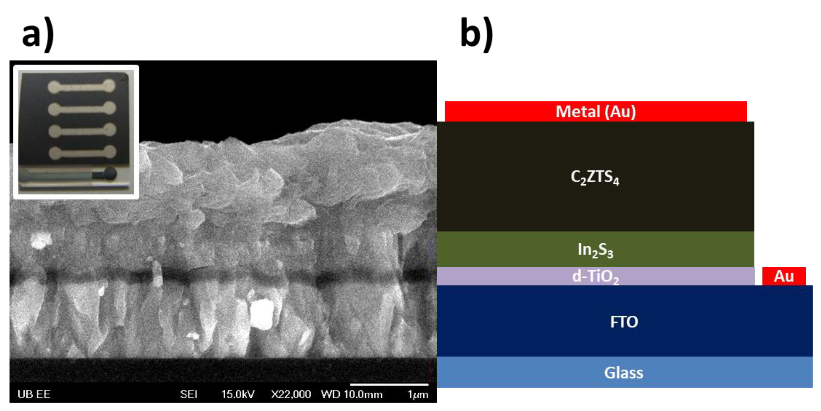
The TiO2 window layer and In2S3 buffer layer thicknesses were controlled by solution concentration and spraying cycles. A TiO2 layer was used for the window layer instead of a conventional ZnO because ZnO has poor chemical stability in acidic conditions, and the spraying solutions for the buffer layer are acidic (pH~5). Figure S1 shows the TiO2 thickness measured from cross-section scanning electron microscopy (SEM) images at different TAA concentrations. We used 80 mM TAA solution for 40 nm of the TiO2 window layer, similar to the intrinsic ZnO layer used in CIGS2 solar cells [23]. Figure S2 presents the thickness of In2S3 buffer layer for various numbers of spraying cycles. We used 40 spraying cycles for 280 nm of the In2S3 buffer layer, which was thicker than the buffer layer of conventional CIGS2 solar cells (~45 nm). Since the following absorber layer was deposited at high temperature (>360 °C) for 30 min, the buffer layer should be thick enough to block the inter-diffusion of elements from the absorber to the transparent conducting oxide layer. However, the thick buffer layer can degrade the total series resistance and solar cell performance. A metal electrode with gold (Au, 30 nm) and silver (Ag, 70 nm) was deposited by electron beam evaporation over 4.25 × 10⁻² cm2. The initial thin Au layer was used for matching the energy level between the valence band of C2ZTS4 and metal, and the second thick Ag layer was to enhance the contact property between the device electrodes and the measurement probes. The light was incident on the device through the FTO-coated glass substrate. Figure 2 shows the cross-section SEM image, a typical sequential structure of an entirely fabricated C2ZTS4 solar cell, and a plan view device photograph (inset), showing the anode contact and the four short cathodes.
In the compositional study of sprayed C2ZTS4 layer, we fixed the substrate temperature at 360 °C and varied the Cu/(Zn + Sn) ratio of the solution from 0.6 to 1.26. We made four solutions in DI water for the main elements: CuCl2 (0.09 M), Zn(CH3CO2)2·2H2O (0.045 M), SnCl4 (0.04 M), and thiourea (0.5 M). The amount of CuCl2 solution was varied from 3 mL to 7 mL to change the Cu/(Zn + Sn) atomic ratio. The spraying solution was made by mixing 5 mL of each solution with the 3 mL to 7 mL CuCl2 and adding DI water to 100 mL. The composition of the main elements of the C2ZTS4 film was measured by energy-dispersive X-ray spectroscopy (EDX). X-ray diffraction (XRD) measurements were performed with 40 kV and 44 mA of voltage and current, respectively. The current-voltage (I-V) characteristic was measured using a Keithley 2400 source meter under calibrated AM 1.5G 1-sun (100 mW/cm2, Oriel) illumination. A 150 W Xenon lamp with Oriel 68805 universal power supply, monochromator (SpectraPro 2300i, Teledyne Prinston Instruments, Trenton, NJ, USA), and a Keithley 6485 picoammeter were used for the external quantum efficiency (EQE) measurement.
3. Results and Discussions
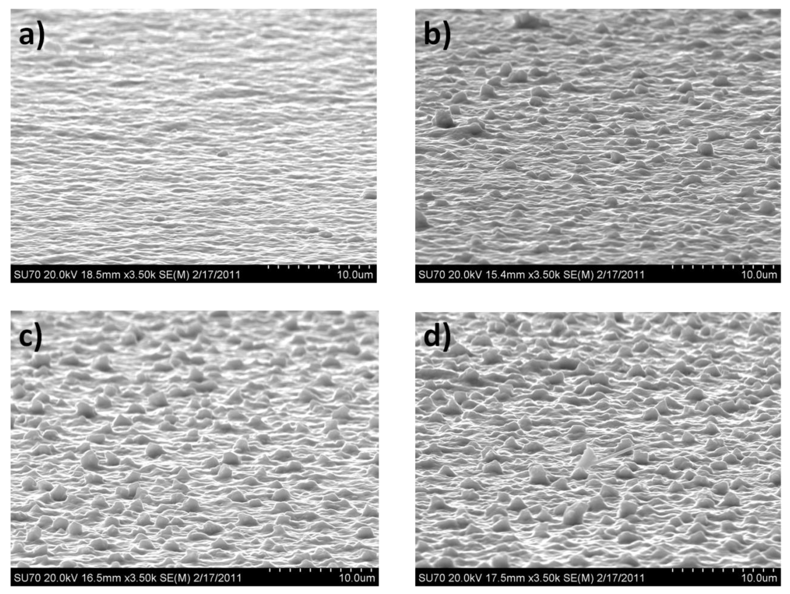
The surface of the C2ZTS4 films deposited by evaporation, sputtering, spraying, or other deposition methods showed rough characteristics [8,13]. The sprayed C2ZTS4 films in this study had a rough surface and different surface characteristics depending on the copper content of the spraying solution. Figure 3 shows the surface SEM images for four copper concentrations. As the copper concentration increased, spherical bumps were created, and the size of the bumps increased. The film composition was measured by EDX and from the cross-section SEM images. It was close to the stoichiometric condition when the Cu/(Zn + Sn) ratio was close to unity. Cu/(Zn + Sn) ratio of 0.8 in the film has been reported as the best condition for high device performance [24]. The relationship between metal element ratio and solar cell device performance is similar for CIGS2 solar cells [15]. When the Cu/(In + Ga) ratio is higher than the optimum condition and close to unity, the bulk absorber layer property is degraded. Lee et al. studied the CIGS2 absorber layer property by using various electrical characterization methods. It showed a high capacitance value, steep slope of capacitance versus log frequency, and low free carrier density at room temperature. Once the Cu/(In + Ga) ratio exceeds the optimum condition, the short-circuit current density (JSC) and open-circuit voltage (VOC) decrease [25].
Spherical bumps were created as the Cu/(Zn + Sn) ratio increased. The copper concentration of the bumps is much higher than that of the flat film area. Since copper has a high diffusion coefficient at high temperature, the copper atoms diffuse out to the surface during layer deposition. Table 1 shows the solution composition, EDX results of the film composition, and the compositional analysis of the bump area. As the Cu/(Zn + Sn) ratio increased, the Cu-rich bump size also increased. A non- uniform composition distribution at the surface as well as rough surfaces are not suitable for the deposition of the next layer. Moreover, the rough surface characteristic of the absorber layer degrades the device performance due to the unstable junction formation at the irregular interface between the absorber and the buffer layer. Therefore, we used the inverse stacking sequence structure (superstrate structure) as shown in Figure 2 instead of the conventional CIGS2 structure to circumvent the device performance degradation due to the inferior surface characteristics of the sprayed C2ZTS4 absorber layer.
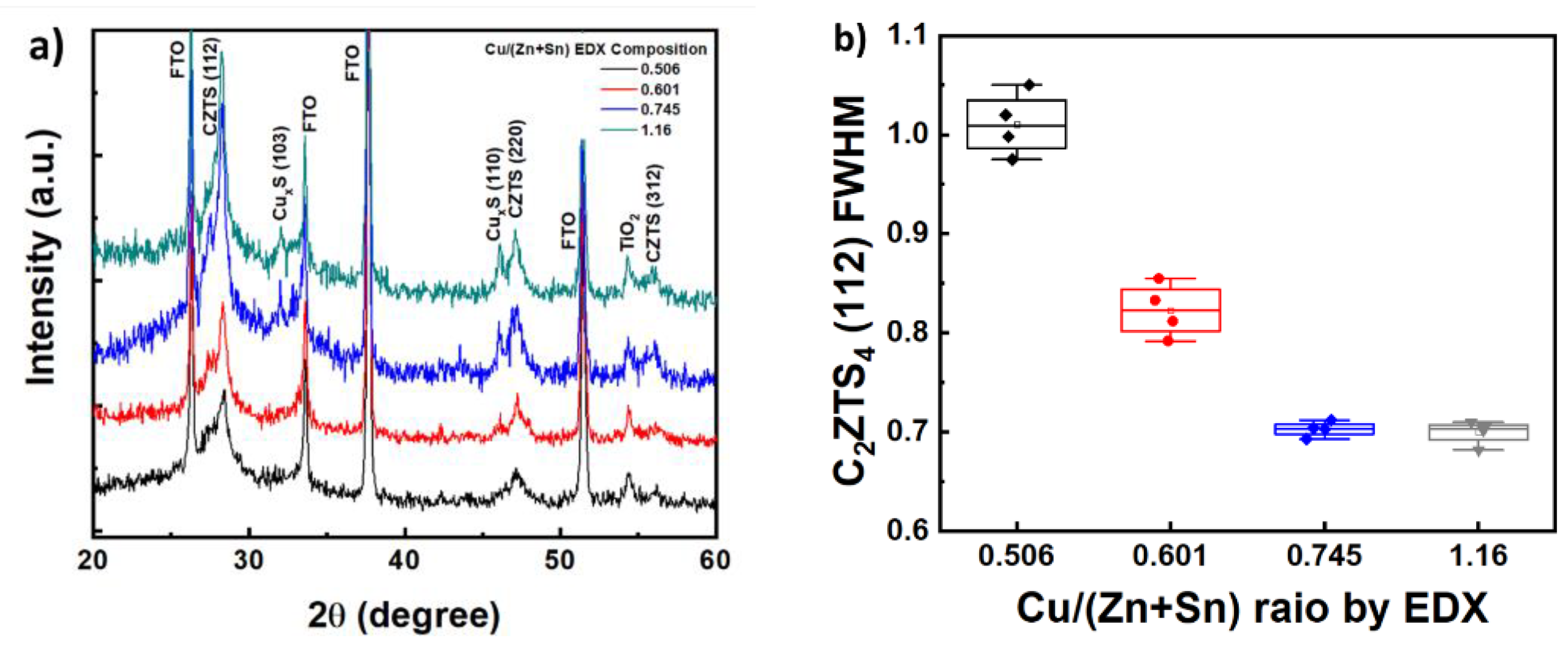
The C2ZTS4 absorber layers were characterized using XRD analysis. As shown in Figure 4, the C2ZTS4 film was successfully created on the FTO/TiO2 substrate. However, when the Cu/(Zn + Sn) ratio was higher than 0.506, the secondary peak around 46.1° increased due to the low formation energy of the CuxS phase. When the Cu/(Zn + Sn) ratio was close to 0.8, a characteristic peak around 28.3° of C2ZTS4 film became distinct compared to that of samples with low Cu/(Zn + Sn) ratio. A sharp peak of the secondary phase (CuxS) also appeared around 46.1° when the Cu content increased. The formation energy of the CuxS phase is lower than that of the C2ZTS4 form. The increase in the CuxS secondary phase peak intensity, shown in Figure 3, is caused by the creation of high Cu-content bumps on the surface. These secondary phases degrade the junction quality between the buffer layer and the absorber layer, resulting in reduced VOC and JSC because they serve as recombination centers in the absorber layer. Although the secondary phase appears on the absorber layer surface, the full width at half maximum (FWHM) of the main C2ZTS4 peak (112) decreased to 0.702° with increasing Cu/(Zn + Sn) ratio. Thus, a higher metallic component ratio produces a higher crystal quality of the polycrystalline C2ZTS4 layer. However, FWHM does not decrease further once the Cu/(Zn + Sn) ratio reaches ~0.75. Therefore, we fixed the solution concentration with a 0.745 Cu/(Zn + Sn) ratio.
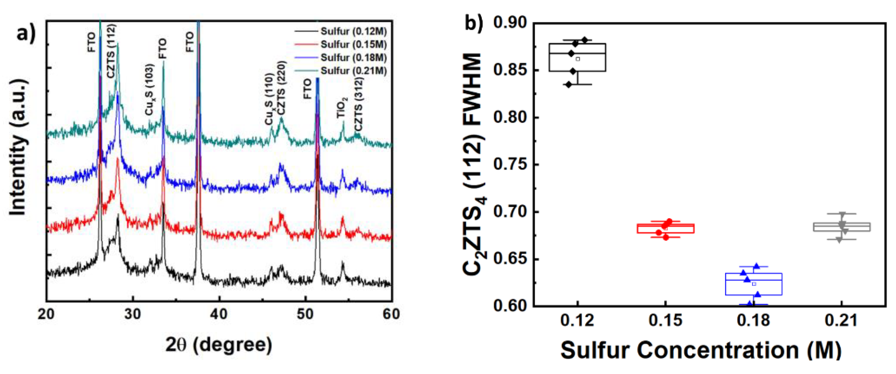
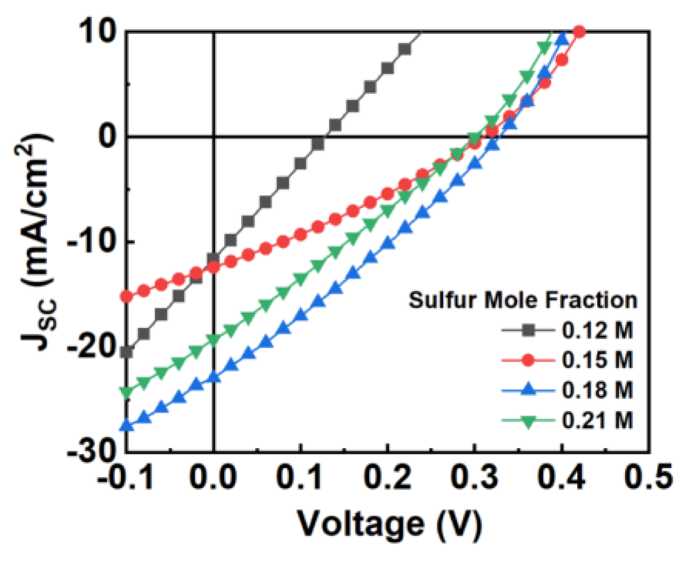
As we observed in the previous studies [22,24,25], the chalcogen element flux and amount of source material is a critical factor for the quality of the absorber layer. We investigated the effect of sulfur concentration in the spraying solution on the final C2ZTS4 absorber film quality. The sulfur concentration was varied from 0.12 M to 0.21 M while the metallic precursor concentration was fixed. The film was deposited on a 360 °C heated FTO substrate. Figure 5 shows the XRD result of the absorber layer deposited with different sulfur concentrations. The deposited C2ZTS4 films showed main (112) and (220) peaks around 28.2° and 47.2°, respectively. The main (112) peak intensity increased at higher sulfur concentrations. However, the FWHM decreased with increasing sulfur concentration, then increased again when the sulfur concentration exceeded the optimum condition. Based on the FWHM changes, 0.18 M S appears to be optimal.
We investigated the electrical characteristics of entirely fabricated devices. Figure 6 shows the current-voltage results. The generated JSC and VOC increased up to 22 mA/cm2 and 328 mV, respectively, at 0.18 M sulfur. The change of JSC and VOC is well-matched with the variation of the FWHM in the XRD results, which reflects the absorber layer quality based on the sulfur concentration. Even for sulfur concentration in the absorber layer over the optimum condition (0.18 M), there was no degradation in the fill factor (FF). It means that the physical and chemical junction characteristic between the In2S3 buffer and C2ZTS4 absorber are not affected by sulfur concentration. The extracted device parameters are listed with the film XRD FWHM values in Table 2.
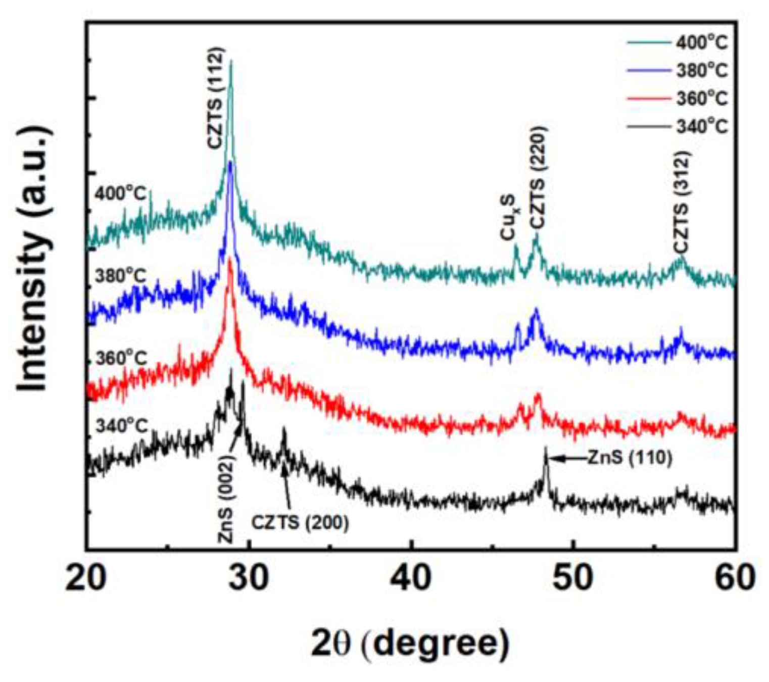
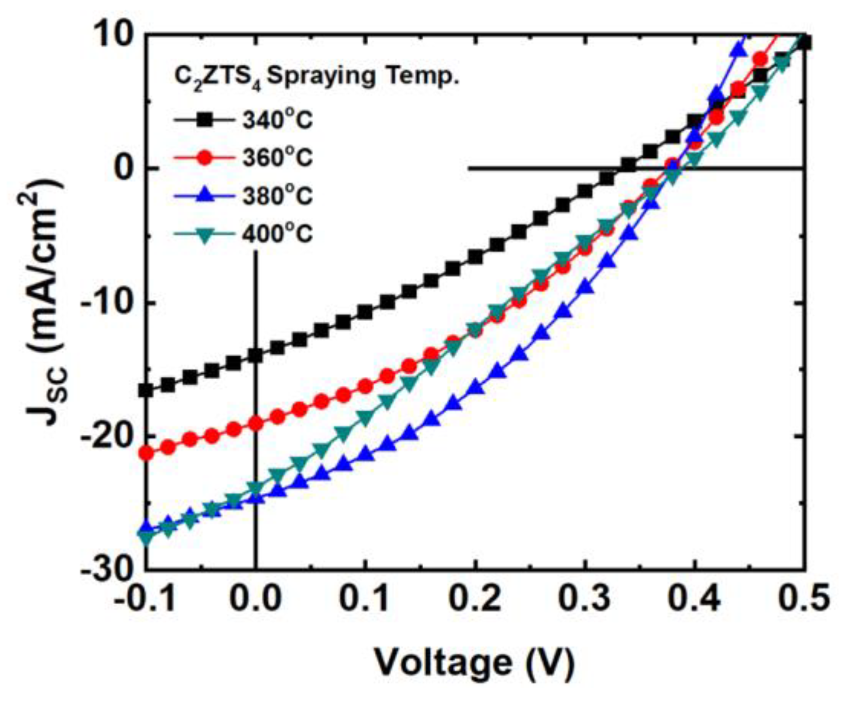
The conventional CIGS2 solar cell structure has a stacking sequence of glass/Mo/CIGS/CdS/ZnO/metal following the so-called substrate structure. Since the CIGS2 layer requires a selenization process at high temperature (above 500 °C), the p-n junction performance between CdS and CIGS2 would be degraded during the high-temperature selenization process if the CIGS2 is deposited on the CdS buffer layer. Therefore, the CIGS2 absorber layer should be created on the Mo back contact first, and the CdS buffer layer coated next. Because the absorber layer of the devices is deposited after the buffer layer, the effect of the deposition temperature of the C2ZTS4 absorber layer should be investigated in detail. We used four temperatures to deposit the absorber layers (340 °C, 360 °C, 380 °C, and 400 °C) using the optimum composition of Cu, Zn, Sn, and S. The deposited C2ZTS4 films were characterized by XRD, as shown in Figure 7. Current–voltage characteristics of the resulting devices are presented in Figure 8, and the extracted solar cell parameters are listed in Table 3 for different spraying temperatures of the C2ZTS4 absorber layer. The C2ZTS4 film deposited at a low deposition temperature (340 °C) shows poor crystal quality, and the secondary phase (ZnS) is present. The film has a rough surface morphology and is delaminated from the substrate, which was also observed in the previous CIGS2 solar cell study [25]. Therefore, the devices processed at low-temperature show low JSC and FF, as well as low VOC, compared to the devices processed at higher temperatures.
In contrast, high-temperature processing (400 °C) yields better C2ZTS4 crystal quality with better FWHM and adhesion. However, the device performance of the high-temperature device is degraded by a low FF. Three hypotheses can explain the degradation of FF from high-temperature spraying. One is the degradation of the absorber layer due to the creation of secondary phases. XRD results show the secondary phases such as ZnS or CuxS, and these could be recombination centers decreasing FF. If the secondary phases degrade the bulk absorber layer, it causes low photocurrent generation as well as FF. The FF drops without significant loss of JSC at 400 °C. Therefore, we can conclude that there is no absorber layer degradation. Another plausible explanation for the decreased FF is junction degradation by the high-temperature process. High temperature can enhance the interaction between the In2S3 buffer layer and the C2ZTS4 absorber layer by the diffusion of high-mobility atoms. As shown in Table 3, the shunt resistances, which are extracted from −0.2 V to 0 V, increased from low temperature to 380 °C and decreased significantly at 400 °C. It means that the leakage current at the junction is increased during photocurrent generation in the devices processed at high temperatures. The last possibility is contact degradation between C2ZTS4 and the final metal contact. Investigation with one-dimensional numerical simulation has shown that higher Schottky barrier heights between layers have significant effects on FF [26,27]. In this study, the surface of the C2ZTS4 layer processed at high temperatures can be easily oxidized before depositing the metal contact. The oxide interface can be an electrical barrier, resulting in the inflection of the I–V curve between JSC and VOC.
As we can see in the 400 °C results, there is no noticeable degradation in JSC and VOC. However, the fluctuation of the I–V curve degrades FF. We concluded that the high-temperature process (400 °C) degrades the junction characteristics and surface contact resistance. Therefore we determined the optimum spraying temperature range for the C2ZTS4 absorber layer to be 360–380 °C. Table 3 lists the general electrical parameters, the extracted shunt resistance, and the FWHM variation of XRD results.
The high series resistance (Rs) in the solar cells hass a profoundly negative impact on FF. As we mentioned in the experimental section, a thick In2S3 buffer layer ~300 nm, was used to prevent the diffusion of elements during the C2ZTS4 layer spraying. However, the thick buffer causes high Rs, and the best cell in this study shows higher than 6 ohms of Rs, calculated by using the one-diode model equation [28]. Silicon and CIGS2 based solar cells are usually within a range of 0.1–2 ohm of Rs. Because of the high Rs, the FF of this study is significantly lower than other solar cells.
Further investigations for reducing the thickness of the buffer layer should be carried out. One possible way is to make a thin buffer layer with a blocking layer. Because of the introduction of the blocking layer, the buffer layer should be thin (<10 nm) to compensate for the total series resistance. We can deposit the buffer layer at less than 10 nm of thickness with chemical bath deposition(CBD) or the atomic layer deposition (ALD) method and grow the thin diffusion-blocking layer (<5 nm) that the carrier can tunnel through. This would be the next study in order to reduce the series resistance of spray C2ZTS4 solar cells.
4. Summary
We successfully fabricated C2ZTS4 solar cells using a low-cost spray-CVD technique. The structure is an inverse stacking sequence of conventional CIGS2 solar cells, and all layers from bottom to top are created by a spraying method. C2ZTS4 solar cells with different metal compositions were investigated with XRD, EDX, and I–V characteristics. The C2ZTS4 absorber layer film characteristics were studied for various Cu/(Zn + Sn) ratios and sulfur concentrations. Cu-poor films have smooth surface characteristics. The C2ZTS44 film from Cu-rich solution yields rough surfaces that contain Cu- rich spherical bumps and flat regions with stoichiometric composition. The film from a Cu-rich solution exhibits a better entire crystal quality for the absorber layer. When the Cu/(Zn + Sn) ratio is close to 0.8, the C2ZTS4 film has a narrow and sharp (112) XRD peak. The sulfur concentration in the spraying solution should be high enough to obtain a quality C2ZTS4 film. However, when it exceeds the optimum condition, VOC and JSC are degraded. High sulfur does not affect the junction formation between the buffer and absorber layer without FF degradation. Growth temperatures for C2ZTS4 absorber layers were studied with four different spraying temperatures. We found the optimum growth temperature range of the C2ZTS4 absorber layer to be 360–380 °C. Lower temperature yields a low quality of absorber film, resulting in low JSC. Devices fabricated at high temperatures (>380 °C) show low FF without degradation of VOC and JSC due to junction degradation and high contact resistance between the absorber layer and metal contact. The best device has 383 mV VOC, 24.6 mA/cm2 JSC, 37.7% FF, and 3.34% efficiency. C2ZTS4 solar cells with spray deposition would be a good candidate for a low-cost mass production process. However, the aqueous-based solution, which is used in this study, can cause surface oxidation and limit grain growth resulting in low device performance. Therefore, further studies for reducing the oxidation and prohibiting the creation of secondary phases should be carried out. One of the possible ways is to spray under a non-oxidation condition such as spraying in a nitrogen box. If we apply this method for the substrate structure solar cells, a surface treatment process to remove the CuxS phase created at the surface of the high Cu/(Zn + Sn) ratio absorber layer should be developed. An interface treatment study is also needed to clarify the advantages of the spraying method for solar cell fabrication.
Supplementary Materials
The following are available online at https://www.mdpi.com/2079-6412/10/6/548/s1, Figure S1: TiO2 thickness vs. concentration of TAA solution. Thickness is extracted from the SEM measured results on FTO (temperature 450 °C, pressure 10 psi, spray 40 cycles), Figure S2: In2S3 thickness vs. the number of spraying cycles. Thickness is extracted from the scanning electron microscopy (SEM) measured results on FTO (temperature 350 °C, solution InCl4 (12 mM) + thiourea (80 mM), pressure 6 psi).
Author Contributions
Conceptualization, D.L.; methodology, D.L.; software, D.L.; validation, J.Y.Y.; formal analysis, D.L.; investigation, D.L.; resources, J.Y.Y.; data curation, D.L.; writing—original draft preparation, D.L.; writing—review and editing, J.Y.Y.; visualization, D.L.; supervision, J.Y.Y.; project administration, D.L.; funding acquisition, D.L., and J.Y.Y. All authors have read and agreed to the published version of the manuscript.
Funding
This research was financially supported by the Air Force Office of Scientific Research (Grant No. FA9550091036) and the National Science Foundation (Grant No. DMR0702372). This research was supported by the Basic Science Research Program through the National Research Foundation of Korea (NRF) funded by the Ministry of Science, ICT & Future Planning (NRF-2019R1A2C4070248).
Conflicts of Interest
The authors declare no conflict of interest.
References
- Ito, K.; Nakazawa, T. Electrical and Optical Properties of Stannite-Type Quaternary Semiconductor Thin Films. Jpn. J. Appl. Phys. 1988, 27, 2094–2097. [Google Scholar] [CrossRef]
- Katagiri, H.; Ishigaki, N.; Ishida, T.; Saito, K. Characterization of Cu2ZnSnS4 Thin Films Prepared by Vapor Phase Sulfurization. Jpn. J. Appl. Phys. 2001, 40, 500–504. [Google Scholar] [CrossRef]
- Moriya, K.; Tanaka, K.; Uchiki, H. Fabrication of Cu2ZnSnS4 Thin-Film Solar Cell Prepared by Pulsed Laser Deposition. Jpn. J. Appl. Phys. 2007, 46, 5780–5781. [Google Scholar] [CrossRef]
- Riha, S.C.; Parkinson, B.A.; Prieto, A.L. Solution-Based Synthesis and Characterization of Cu2ZnSnS4 Nanocrystals. J. Am. Chem. Soc. 2009, 131, 12054–12055. [Google Scholar] [CrossRef]
- Tanaka, K.; Oonuki, M.; Moritake, N.; Uchiki, H. Cu2ZnSnS4 thin film solar cells prepared by non-vacuum processing. Sol. Energy Mater. Sol. Cells. 2009, 93, 583–587. [Google Scholar] [CrossRef]
- Wang, W.; Winkler, M.T.; Gunawan, O.; Gokmen, T.; Todorov, T.K.; Zhu, Y.; Mitzi, D.B. Device Characteristics of C2ZTS4Se Thin-Film Solar Cells with 12.6% Efficiency. Adv. Energy Mater. 2014, 4, 1301465. [Google Scholar] [CrossRef]
- Schubert, B.A.; Marsen, B.; Cinque, S.; Unold, T.; Klenk, R.; Schorr, S.; Schock, H.W. Cu2ZnSnS4 thin film solar cells by fast coevaporation. Prog. Photovolt. Res. Appl. 2011, 19, 93–96. [Google Scholar] [CrossRef]
- Araki, H.; Mikaduki, A.; Kubo, Y.; Sato, T.; Jimbo, K.; Maw, W.S.; Katagiri, H.; Yamazaki, M.; Oishi, K.; Takeuchi, A. Preparation of Cu2ZnSnS4 thin films by sulfurization of stacked metallic layers. Thin Solid Films. 2008, 517, 1457–1460. [Google Scholar] [CrossRef]
- Guo, Q.; Hillhouse, H.W.; Agrawal, R. Synthesis of Cu2ZnSnS4 Nanocrystal ink and its use for solar cells. J. Am. Chem. Soc. 2009, 131, 11672–11673. [Google Scholar] [CrossRef]
- Steinhagen, C.; Panthani, M.G.; Akhavan, V.; Goodfellow, B.; Koo, B.; Korgel, A. Synthesis of Cu2ZnSnS4 Nanocrystals for Use in Low-Cost Photovoltaics. J. Am. Chem. Soc. 2009, 131, 12554–12555. [Google Scholar] [CrossRef]
- Deokate, R.J.; Adsool, A.D.; Shinde, N.S.; Pawar, S.M.; Lokhande, C.D. Structural and Optical Properties of Spray-deposited Cu2ZnSnS4 thin film. Energy Procedia 2014, 54, 627–633. [Google Scholar] [CrossRef] [Green Version]
- Diwate, K.; Mohite, K.; Shinde, M.; Rondiya, S.; Pawbake, A.; Date, A.; Pathan, H.; Jadkar, S. Synthesis and Characterization of Chemical Spray Pyrolysed C2ZTS4 Thin Films for Solar Cell Application. Energy Procedia 2017, 110, 180–187. [Google Scholar] [CrossRef]
- Nguyen, T.H.; Septina, W.; Fujikawa, S.; Jiang, F.; Harada, T.; Ikeda, S. Cu2ZnSnS4 thin film solar cells with 5.8% conversion efficiency obtained by a facile spray pyrolysis technique. RSC Adv. 2015, 5, 77565–77571. [Google Scholar] [CrossRef]
- Prabhakar, T.; Jampana, N. Effect of sodium diffusion on the structural and electrical properties of Cu2ZnSnS4 thin films. Sol. Energy Mater. Sol. Cells. 2011, 95, 1001–1004. [Google Scholar] [CrossRef]
- Nam, J.; Kan, Y.; Lee, D.; Yang, J.; Kim, Y.; Mo, C.B.; Park, S.; Kim, D. Achievement of 17.9% Efficiency in 30 × 30 cm2 Cu(In,Ga)(Se,S)2 Solar Cell Sub-Module by Sulfurization after Selenization with Cd-Free Buffer. Prog. Photovolt. Res. Appl. 2016, 24, 175–182. [Google Scholar] [CrossRef]
- Chen, C.H.; Shih, W.C.; Chien, C.Y.; Hsu, C.H.; Wu, Y.H.; Lai, C.H. A promising sputtering route for one-step fabrication of chalcopyrite phase Cu(In,Ga)Se2 absorbers without extra Se supply. Sol. Energy Mater. Sol. Cells 2012, 103, 25–29. [Google Scholar] [CrossRef]
- Ma, Q.; Zhang, W.; Jiang, Z.; Ma, D.; Zhang, Y.; Lu, C.; Fan, Z. The Formation Mechanism of Cu(In0.7Ga0.3)Se2 Nanoparticles and the Densification Trajectory of the Se-Rich Quaternary Target by Hot Pressing. Crystals 2018, 8, 135. [Google Scholar] [CrossRef] [Green Version]
- Wang, K.; Gunawan, O.; Todorov, T.; Shin, B.; Chey, S.J.; Bojarczuk, N.A.; Mitzi, D.; Guha, S. Thermally evaporated Cu2ZnSnS4 solar cells. Appl. Phys. Lett. 2010, 97, 143508. [Google Scholar] [CrossRef]
- Embden, J.V.; Chesman, A.S.R.; Gaspera, E.D.; Duffy, N.W.; Watkins, S.E.; Jasieniak, J.J. Cu2ZnSnS4xSe4(1–x) Solar Cells from Polar Nanocrystal Inks. J. Am. Chem. Soc. 2014, 136, 5237–5240. [Google Scholar] [CrossRef]
- Vigil-Galán, O.; Courel, M.; Espindola-Rodriguez, M.; Izquierdo-Roca, V.; Saucedo, E.; Fairbrother, A. Toward a high Cu2ZnSnS4 solar cell efficiency processed by spray pyrolysis method. J. Renew. Sustain. Energy. 2013, 5, 053137. [Google Scholar]
- Kavan, L.; Grätzel, M. Highly efficient semiconducting TiO2 photoelectrodes prepared by aerosol pyrolysis. Electrochim. Acta. 1995, 40, 643–652. [Google Scholar] [CrossRef]
- Pai, R.R.; John, T.T.; Kashiwaba, Y.; Abe, T.; Vijayakumar, K.P.; Kartha, C.S. Defect characterization of spray pyrolyzed β-In2S3 thin film using Thermally Stimulated Current measurements. J. Mater. Sci. 2005, 40, 741–746. [Google Scholar] [CrossRef]
- Repins, I.; Contreras, M.A.; Egaas, B.; DeHart, C.; Scharf, J.; Perkins, C.L.; To, B.; Noufi, R. 19.9%-efficient ZnO/CdS/CuInGaSe2 solar cell with 81.2% fill factor. Prog. Photovolt. Res. Appl. 2008, 16, 235–239. [Google Scholar] [CrossRef] [Green Version]
- Katagiri, H.; Jimbo, K.; Maw, W.S.; Oishi, K.; Yamazaki, M.; Araki, H.; Takeuchi, A. Development of C2ZTS4-based thin film solar cells. Thin Solid Films. 2009, 517, 2455–2460. [Google Scholar] [CrossRef]
- Lee, D.; Lee, J.; Kim, Y.; Mo, C.B.; Lee, D.; Yang, J.; Nam, J.; Beak, D.; Park, S.; Kim, B.; et al. Effects of the Cu/(Ga + In) Ratio on the Bulk and Interface Properties of Cu(InGa)(SSe)2 Solar Cells. Sol. Energy Mater. Sol. Cells. 2016, 149, 195–203. [Google Scholar] [CrossRef]
- Hsiao, K.; Liu, J.; Hsieh, H.; Jiang, T. Electrical impact of MoSe2 on CIGS thin-film solar cells. Phys. Chem. Chem. Phys. 2013, 15, 18174–18178. [Google Scholar] [CrossRef]
- Sun, H.; Li, P.; Xue, Y.; Qiao, Z.; Sai, L. Effect of MoSe2 on the performance of CIGS solar cells. Optoelectron. Lett. 2019, 15, 428–434. [Google Scholar] [CrossRef]
- Mehta, H.K.; Warke, H.; Kukadiya, K.; Panchal, A.K. Accurate expression for single-diode-model solar cell pararmeterization. IEEE J. Photovolt. 2019, 9, 803–810. [Google Scholar] [CrossRef]
Figure 1.
Schematic diagram of the spraying system.

Figure 2.
(a) Cross-section scanning electron microscopy (SEM) image of the C2ZTS4 solar cell and device photograph (inset) and (b) corresponding layer structure plan view.
Figure 2.
(a) Cross-section scanning electron microscopy (SEM) image of the C2ZTS4 solar cell and device photograph (inset) and (b) corresponding layer structure plan view.

Figure 3.
C2ZTS4 scanning electron microscopy (SEM) surface images at Cu/(Zn + Sn) ratios of (a) 0.63, (b) 0.90, (c) 1.08, and (d) 1.26.
Figure 3.
C2ZTS4 scanning electron microscopy (SEM) surface images at Cu/(Zn + Sn) ratios of (a) 0.63, (b) 0.90, (c) 1.08, and (d) 1.26.

Figure 4.
(a) X-ray diffraction (XRD) results of the C2ZTS4 layers and (b) full width at half maximum (FWHM) of the main C2ZTS4 (112) peak for four Cu/(Zn + Sn) ratios.
Figure 4.
(a) X-ray diffraction (XRD) results of the C2ZTS4 layers and (b) full width at half maximum (FWHM) of the main C2ZTS4 (112) peak for four Cu/(Zn + Sn) ratios.

Figure 5.
(a) X-ray diffraction (XRD) results of the C2ZTS4 layers and (b) full width at half maximum (FWHM) of the main C2ZTS4 (112) peak for four spraying solution sulfur concentrations.
Figure 5.
(a) X-ray diffraction (XRD) results of the C2ZTS4 layers and (b) full width at half maximum (FWHM) of the main C2ZTS4 (112) peak for four spraying solution sulfur concentrations.

Figure 6.
Current-voltage characteristics for various sulfur concentrations in the C2ZTS4 spraying solution.
Figure 6.
Current-voltage characteristics for various sulfur concentrations in the C2ZTS4 spraying solution.

Figure 7.
X-ray diffraction (XRD) characteristics of C2ZTS4 absorber layers sprayed at different temperatures.
Figure 7.
X-ray diffraction (XRD) characteristics of C2ZTS4 absorber layers sprayed at different temperatures.

Figure 8.
Current-voltage characteristics for C2ZTS4 layers sprayed at different temperatures.


Table 1.
Composition of the spraying solution and Cu/(Zn + Sn) ratio measured by EDX at the inside of the C2ZTS4 film.
Table 1.
Composition of the spraying solution and Cu/(Zn + Sn) ratio measured by EDX at the inside of the C2ZTS4 film.
| Solution | Solution Composition | Film Comp. (EDX) | Bump (EDX) | |||
|---|---|---|---|---|---|---|
| Cu | Zn | Sn | Cu/(Zn + Sn) | Cu/(Zn + Sn) | Cu/(Zn + Sn) | |
| #1 | 1.26 | 1 | 1 | 0.63 | 0.506 | N/A |
| #2 | 1.8 | 1 | 1 | 0.9 | 0.601 | 1.19 |
| #3 | 2.16 | 1 | 1 | 1.08 | 0.745 | 3.43 |
| #4 | 2.52 | 1 | 1 | 1.26 | 1.16 | 4.41 |
Table 2.
Device parameters at various spraying solution sulfur concentrations.
| Sulfur Mole Fraction | VOC (mV) | JSC (mA/cm2) | FF (%) | PCE (%) | CZTS (112) FWHM (o) |
|---|---|---|---|---|---|
| 0.12 M | 128 | 11.65 | 28.2 | 0.42 | 0.868 |
| 0.15 M | 312 | 12.39 | 29.8 | 1.15 | 0.687 |
| 0.18 M | 328 | 22.91 | 28.4 | 2.13 | 0.628 |
| 0.21 M | 305 | 19.26 | 28.3 | 1.66 | 0.685 |
Table 3.
Extracted device parameters for C2ZTS4 sprayed at various temperatures.
| Temperature | VOC (mV) | JSC (mA/cm2) | FF (%) | PCE (%) | Rsh (Ω·cm2) | CZTS (112) FWHM (o) |
|---|---|---|---|---|---|---|
| 340 °C | 333 | 13.93 | 30.2 | 1.34 | 37.9 | 0.868 |
| 360 °C | 381 | 19.02 | 35.2 | 1.60 | 45.3 | 0.687 |
| 380 °C | 383 | 24.6 | 37.7 | 3.34 | 44.8 | 0.628 |
| 400 °C | 386 | 23.8 | 27.9 | 2.4 | 26.9 | 0.685 |
© 2020 by the authors. Licensee MDPI, Basel, Switzerland. This article is an open access article distributed under the terms and conditions of the Creative Commons Attribution (CC BY) license (http://creativecommons.org/licenses/by/4.0/).
Share and Cite
MDPI and ACS Style
Lee, D.; Yang, J. Superstrate Structured FTO/TiO2/In2S3/Cu2ZnSnS4 Solar Cells Fabricated by a Spray Method with Aqueous Solutions. Coatings 2020, 10, 548. https://doi.org/10.3390/coatings10060548
AMA Style
Lee D, Yang J. Superstrate Structured FTO/TiO2/In2S3/Cu2ZnSnS4 Solar Cells Fabricated by a Spray Method with Aqueous Solutions. Coatings. 2020; 10(6):548. https://doi.org/10.3390/coatings10060548
Chicago/Turabian StyleLee, Dongho, and JungYup Yang. 2020. "Superstrate Structured FTO/TiO2/In2S3/Cu2ZnSnS4 Solar Cells Fabricated by a Spray Method with Aqueous Solutions" Coatings 10, no. 6: 548. https://doi.org/10.3390/coatings10060548
Note that from the first issue of 2016, this journal uses article numbers instead of page numbers. See further details here.